Paper Menu >>
Journal Menu >>
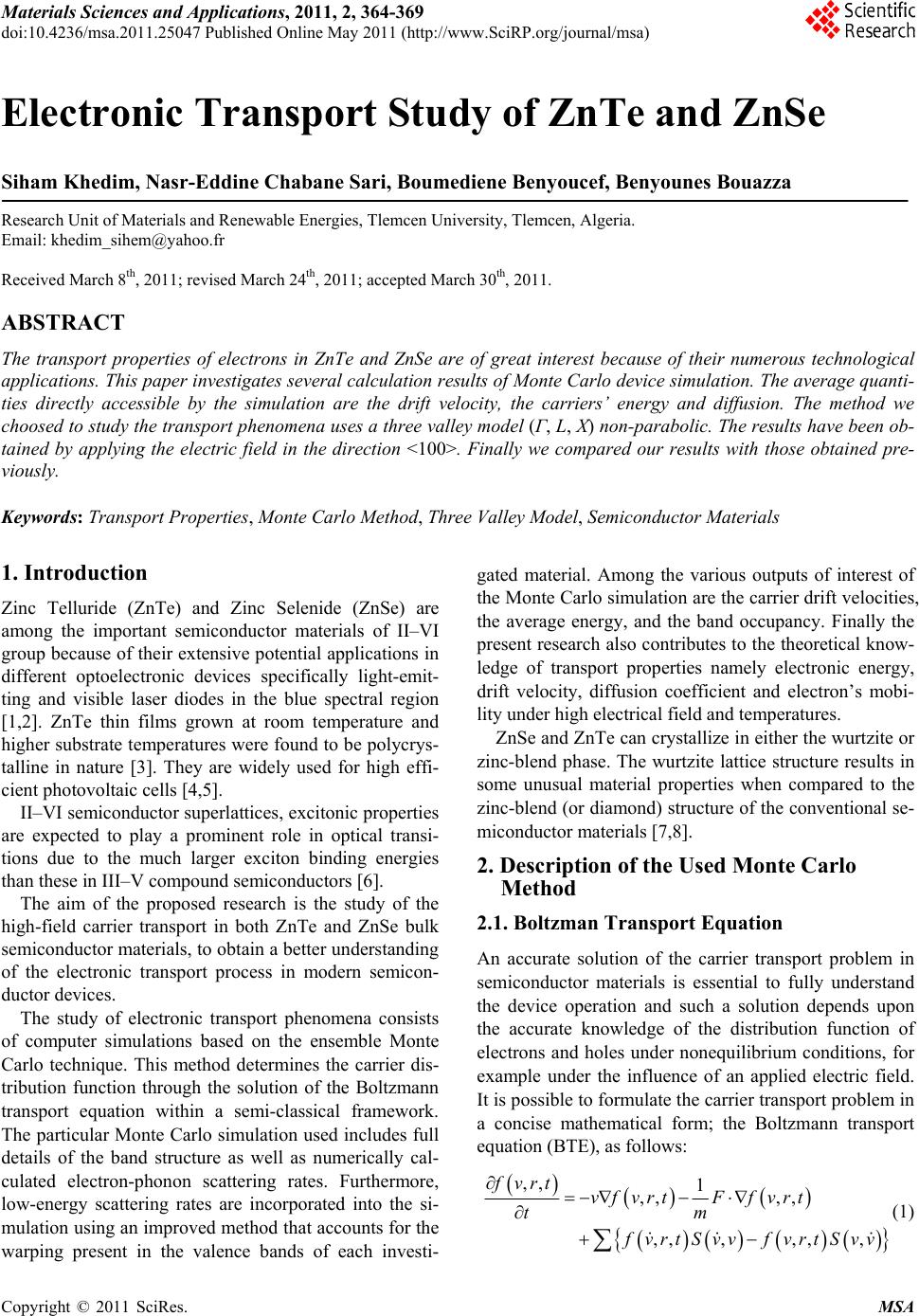 Materials Sciences and Applications, 2011, 2, 364-369 doi:10.4236/msa.2011.25047 Published Online May 2011 (http://www.SciRP.org/journal/msa) Copyright © 2011 SciRes. MSA Electronic Transport Study of ZnTe and ZnSe Siham Khedim, Nasr-Eddine Chabane Sari, Boumediene Benyoucef, Benyounes Bouazza Research Unit of Materials and Renewable Energies, Tlemcen University, Tlemcen, Algeria. Email: khedim_sihem@yahoo.fr Received March 8th, 2011; revised March 24th, 2011; accepted March 30th, 2011. ABSTRACT The transport properties of electrons in ZnTe and ZnSe are of great interest because of their numerous technological applications. This paper investigates several calculation results of Monte Carlo device simulation. The average quanti- ties directly accessible by the simulation are the drift velocity, the carriers’ energy and diffusion. The method we choosed to study the transport phenomena uses a three valley model (Γ, L, X) non-parabolic. The results have been ob- tained by applying the electric field in the direction <100>. Finally we compared our results with those obtained pre- viously. Keywords: Transport Properties, Monte Carlo Method, Three Valley Model, Semiconductor Materials 1. Introduction Zinc Telluride (ZnTe) and Zinc Selenide (ZnSe) are among the important semiconductor materials of II–VI group because of their extensive potential applications in different optoelectronic devices specifically light-emit- ting and visible laser diodes in the blue spectral region [1,2]. ZnTe thin films grown at room temperature and higher substrate temperatures were found to be polycrys- talline in nature [3]. They are widely used for high effi- cient photovoltaic cells [4,5]. II–VI semiconductor superlattices, excitonic properties are expected to play a prominent role in optical transi- tions due to the much larger exciton binding energies than these in III–V compound semiconductors [6]. The aim of the proposed research is the study of the high-field carrier transport in both ZnTe and ZnSe bulk semiconductor materials, to obtain a better understanding of the electronic transport process in modern semicon- ductor devices. The study of electronic transport phenomena consists of computer simulations based on the ensemble Monte Carlo technique. This method determines the carrier dis- tribution function through the solution of the Boltzmann transport equation within a semi-classical framework. The particular Monte Carlo simulation used includes full details of the band structure as well as numerically cal- culated electron-phonon scattering rates. Furthermore, low-energy scattering rates are incorporated into the si- mulation using an improved method that accounts for the warping present in the valence bands of each investi- gated material. Among the various outputs of interest of the Monte Carlo simulation are the carrier drift velocities, the average energy, and the band occupancy. Finally the present research also contributes to the theoretical know- ledge of transport properties namely electronic energy, drift velocity, diffusion coefficient and electron’s mobi- lity under high electrical field and temperatures. ZnSe and ZnTe can crystallize in either the wurtzite or zinc-blend phase. The wurtzite lattice structure results in some unusual material properties when compared to the zinc-blend (or diamond) structure of the conventional se- miconductor materials [7,8]. 2. Description of the Used Monte Carlo Method 2.1. Boltzman Transport Equation An accurate solution of the carrier transport problem in semiconductor materials is essential to fully understand the device operation and such a solution depends upon the accurate knowledge of the distribution function of electrons and holes under nonequilibrium conditions, for example under the influence of an applied electric field. It is possible to formulate the carrier transport problem in a concise mathematical form; the Boltzmann transport equation (BTE), as follows: ,, 1 ,, ,, ,,,,,, fvrt vfvrtF fvrt tm f vrtSvvf vrtSvv (1) 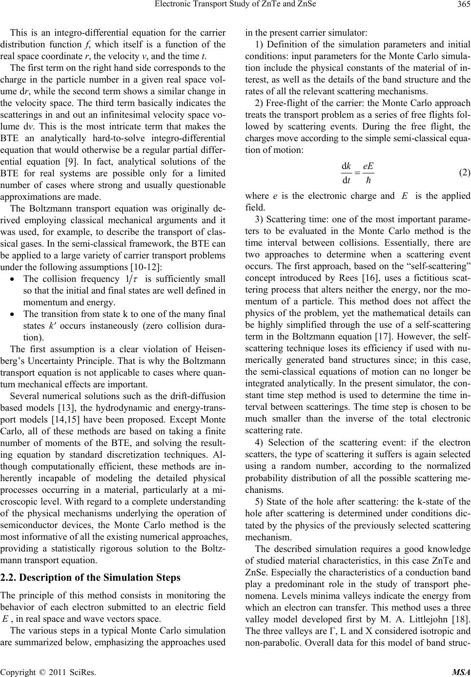 Electronic Transport Study of ZnTe and ZnSe Copyright © 2011 SciRes. MSA 365 This is an integro-differential equation for the carrier distribution function f, which itself is a function of the real space coordinate r, the velocity v, and the time t. The first term on the right hand side corresponds to the charge in the particle number in a given real space vol- ume dr, while the second term shows a similar change in the velocity space. The third term basically indicates the scatterings in and out an infinitesimal velocity space vo- lume dv. This is the most intricate term that makes the BTE an analytically hard-to-solve integro-differential equation that would otherwise be a regular partial differ- ential equation [9]. In fact, analytical solutions of the BTE for real systems are possible only for a limited number of cases where strong and usually questionable approximations are made. The Boltzmann transport equation was originally de- rived employing classical mechanical arguments and it was used, for example, to describe the transport of clas- sical gases. In the semi-classical framework, the BTE can be applied to a large variety of carrier transport problems under the following assumptions [10-12]: The collision frequency 1 is sufficiently small so that the initial and final states are well defined in momentum and energy. The transition from state k to one of the many final states k' occurs instaneously (zero collision dura- tion). The first assumption is a clear violation of Heisen- berg’s Uncertainty Principle. That is why the Boltzmann transport equation is not applicable to cases where quan- tum mechanical effects are important. Several numerical solutions such as the drift-diffusion based models [13], the hydrodynamic and energy-trans- port models [14,15] have been proposed. Except Monte Carlo, all of these methods are based on taking a finite number of moments of the BTE, and solving the result- ing equation by standard discretization techniques. Al- though computationally efficient, these methods are in- herently incapable of modeling the detailed physical processes occurring in a material, particularly at a mi- croscopic level. With regard to a complete understanding of the physical mechanisms underlying the operation of semiconductor devices, the Monte Carlo method is the most informative of all the existing numerical approaches, providing a statistically rigorous solution to the Boltz- mann transport equation. 2.2. Description of the Simulation Steps The principle of this method consists in monitoring the behavior of each electron submitted to an electric field E, in real space and wave vectors space. The various steps in a typical Monte Carlo simulation are summarized below, emphasizing the approaches used in the present carrier simulator: 1) Definition of the simulation parameters and initial conditions: input parameters for the Monte Carlo simula- tion include the physical constants of the material of in- terest, as well as the details of the band structure and the rates of all the relevant scattering mechanisms. 2) Free-flight of the carrier: the Monte Carlo approach treats the transport problem as a series of free flights fol- lowed by scattering events. During the free flight, the charges move according to the simple semi-classical equa- tion of motion: d d keE t (2) where e is the electronic charge and E is the applied field. 3) Scattering time: one of the most important parame- ters to be evaluated in the Monte Carlo method is the time interval between collisions. Essentially, there are two approaches to determine when a scattering event occurs. The first approach, based on the “self-scattering” concept introduced by Rees [16], uses a fictitious scat- tering process that alters neither the energy, nor the mo- mentum of a particle. This method does not affect the physics of the problem, yet the mathematical details can be highly simplified through the use of a self-scattering term in the Boltzmann equation [17]. However, the self- scattering technique loses its efficiency if used with nu- merically generated band structures since; in this case, the semi-classical equations of motion can no longer be integrated analytically. In the present simulator, the con- stant time step method is used to determine the time in- terval between scatterings. The time step is chosen to be much smaller than the inverse of the total electronic scattering rate. 4) Selection of the scattering event: if the electron scatters, the type of scattering it suffers is again selected using a random number, according to the normalized probability distribution of all the possible scattering me- chanisms. 5) State of the hole after scattering: the k-state of the hole after scattering is determined under conditions dic- tated by the physics of the previously selected scattering mechanism. The described simulation requires a good knowledge of studied material characteristics, in this case ZnTe and ZnSe. Especially the characteristics of a conduction band play a predominant role in the study of transport phe- nomena. Levels minima valleys indicate the energy from which an electron can transfer. This method uses a three valley model developed first by M. A. Littlejohn [18]. The three valleys are Γ, L and X considered isotropic and non-parabolic. Overall data for this model of band struc-  Electronic Transport Study of ZnTe and ZnSe Copyright © 2011 SciRes. MSA 366 ture of ZnTe and ZnSe are summarized in the following Table 1. 3. Results and Discussion 3.1. Electronic Energy We present on Figure 1 and Figure 2 the average energy as a function of time for different values of electric field for the cited materials ZnSe and ZnTe. The curves have the same shape. We notice that for strong electric fields the carriers acquire higher energies for same temperature conditions 300 K. Comparing the two curves, one no- tices that the ZnTe reaches higher energies than those in ZnSe for same electric field values. For E = 700 kV/cm, the energy reaches a value of about 200 eV in the case of ZnTe and a value of about 90 eV in the case of ZnSe. We note also that two phases exist. In the first one, the carriers are quickly accelerated and the energy is almost linear. In this time collisions are becoming more numerous, leading to a spread of energy distribution. Thereafter it stabilizes in the second phase, because electrons lost their energy in the collisions. The observed behavior is quite different depending on the temperature of the lattice. At 300 K for electric fields close to zero, the energy of carriers is small and its dis- tribution is little spread out. This means there is practi- cally no carrier susceptible of emitting intervalley pho- nons of high energy. That is to say no carrier energy of which is at least equal to the energy emitted in an inelas- tic collision. It results in a fairly rapid increase of the average energy. When the field increases, all carriers are heated, the energy distribution broadens the number of carriers that emit photons increases and the increase of the average energy with the electric field is lower. At high lattice temperatures this phenomenon is not detect- able because even for low-field, the energy distribution of carriers is sufficiently spread out to permit an impor- Table 1. Data on the band structure of ZnTe and ZnS [19]. ZnTe ZnSe Effective masses * 00.12mm * 00.46 L mm * 00.30 X mm * 00.17mm * 00.51 L mm * 00.32 X mm Levels of the valleys 2.35 eV g E 2.38 eV L E 2.84 eV X E 2.82 eV g E 1.58 eV L E 1.49 eV X E Non-parabolicity coefficient 0.41 0.40 L 0.35 X 0.67 0.43 L 0.20 X Figure 1. Energy variation with time in ZnSe. Figure 2. Energy variation with time in ZnTe. tant emission of very energetic phonons including all types of phonons involved in collisions [20,21]. 3.2. Drift Velocity The curves on Figure 3 and Figure 4 represent the varia- tion of drift velocity as a function of electric field. The curves show the existence of three phases: a rapid and linear increase of the drift velocity followed by a peak and then the decrease of speed until saturation. In fact, the carriers are in the central valley Γ. During phases of free flight, the carriers are subject to the influence of electric field and thus are accelerated because of the low value of effective mass, at the same time they gain en- ergy. Reaching a threshold, such carriers lose their speed and their energy in collisions. And because of interac- tions, electrons will be able to win the necessary energy  Electronic Transport Study of ZnTe and ZnSe Copyright © 2011 SciRes. MSA 367 Figure 3. Drift velocity variation with electric field for ZnSe. Figure 4. Drift velocity variation with electric field for ZnTe. to be transferred from the Γ valley into a side valley L or X. Once carriers will be in high valleys, their energy will converge towards a stationary value since any gained energy by electrons will compensate the energy he has ceded to the crystal lattice. Thus, the drift velocity de- creases until saturation. The over-speed phenomenon was studied by many authors and specific simulations of type Monte Carlo. It appears in semiconductors when subjected to an electric field, one will take into account the transitory effects that exist when electrons are subjected to an electric field [22]. One recognizes a semiconductor material that is sub- ject to any electric field, the distribution of carriers is a Maxwell Boltzmann distribution. Suppose that Time = 0, applying an electric field to electrons has the immediate effect moving electrons representative points in the same direction within the wave-vectors space [17]. 3.3. Coefficient of Diffusion The definitions of the diffusion coefficient by sprawl of a packet and by noise, which do not imply any condition on the field, are applied also for high field. The Monte Carlo methods permit to skirt around the difficulties that present the definition of a diffusion coefficient in high fields. These definitions take into account both the dis- tribution of electrons between the valleys, and transfers. Figure 5 and Figure 6 show the evolution of the dif- fusion coefficient as a function of time in strong field (E = 300 kV/cm). The curve’s shape presents a steep slope, which is traducing both the accelerating action of the field, reinforced by the low value of the effective mass in Central Valley, and the anisotropy due to the dominant interactions which favor speed in the direction parallel to the field. After this first phase, the shape of curves shows satu- Figure 5. Coefficient of diffusion variation with time ZnSe. Figure 6. Coefficient of diffusion variation with time ZnTe.  Electronic Transport Study of ZnTe and ZnSe Copyright © 2011 SciRes. MSA 368 ration. This is explained by the fact that electrons have transferred to the side valleys, and have undergone inter- actions and thus, have lost their excess energy, hence the saturation. 4. Conclusions We have presented a complete material study performed on the ZnSe and ZnTe. It is focused on the characteristics of speed, energy and diffusion coefficient. We have achieved this study from a simulation using Monte Carlo methods that simplify the study of transport phenomena. The application of the simulation led to highlight the evolution of the energy resulting carriers transfer from the central valley to the side valleys, followed by the relaxation phenomenon. Otherwise we have highlighted the phenomenon of over speed. When carriers are accel- erated by the electric field their drift velocity decreases until saturation after transmitting their energy to the crystal lattice or during collisions. We have compared our results with those obtained previously and we think that they are with a good agreement [23-25]. At last, we have defined the mechanisms of diffusion. From the comparison between the two materials we can conclude that ZnSe is best suited for optoelectronic ap- plications, and ZnTe is best suited for photovoltaic ap- plications. REFERENCES [1] D. Stojanovic and R. Kostic, “Quasistationary Electron States for CdTe/ZnTe/CdTe Open Spherical Quantum Dots,” Acta Physica Polonica A, Vol. 117, No. 5, 2010, pp. 768-771. [2] J. Jaeck, “Emission Infrarouge Sous Champ Électrique dans le Cristal de ZnSe Dopé au Chrome,” Ph.D. Dis- sertation, Onera Paristech, Paris, 2009. [3] N. Mazumdar, R. Sarma, B. K. Sarma and H. L. Das, “Photoconductivity of ZnTe Thin Films at Elevated Temperatures,” Bulletin of Materials Science, Vol. 29, No. 1, February 2006, pp. 11-14. doi:10.1007/BF02709347 [4] T. A. Gessert, P. Sheldon, X. Li, D. Dunlavy, D. Niles, R. Sasala, S. Albright and B. Zadler, “Studies of Znte Back Contacts to CdS/CdTe Solar Cells,” Photovoltaic Spe- cialists Conference, Conference Record of the Twen- ty-Sixth IEEE, Anaheim, 1997, pp. 419-422. [5] T. Tanaka, K. M. Yu, P. R. Stone, J. W. Beeman, O. D. Dubon, L. A. Reichertz, V. M. Kao, M. Nishio and W. Walukiewicz, “Demonstration of Homojunction ZnTe Solar Cells,” Journal of Applied Physics, Vol. 108, No. 2, July 2010, Article ID 024502, pp. 1-3. doi:10.1063/1.3463421 [6] J. Bang, J. Park, J.-H. Lee, N. Won, J. Nam, J. Lim, B.-Y. Chang, H.-J. Lee, B. Chon, J. Shin, J.-B. Park, J.-H. Choi, K. Cho, S.-M. Park, T. Joo and S. Kim, “ZnTe/ZnSe (Core/Shell) Type-II Quantum Dots: Their Optical and Photovoltaic Properties,” Chemistry of Materials, Vol. 22, 2010, pp. 233-240. doi:10.1021/cm9027995 [7] A. Ohtake, J. Nakamura, M. Terauchi, F. Sato, M. Tanaka, K. Kimura and T. Yao, “Wurtzite-Zinc-Blende Polytyp- ism in ZnSe on GaAs(111)A,” Physical Review B, Vol. 63, No. 19, 2005, Article ID 195325, pp. 1-4. [8] N. G. Szwacki, “Structural Properties of MnTe, ZnTe and ZnMnTe,” Acta Physica Polonica A, Vol. 106, No. 8, 2004, p. 233. [9] W. Stutius, “Preparation of Low-Resistivity n-Type ZnSe by Organometallic Chemical Vapor Deposition,” Applied Physics Letters, Vol. 38, No. 5, 1981, pp. 352-354. doi:10.1063/1.92374 [10] F. Bogani, S. Grifoni, M. Gurioli and L. Morolli, “Band- Edge Dynamics and Trapping in ZnSe Crystals,” Physical Review B, Vol. 52, No. 4, 1995, pp. 2543-2549. doi:10.1103/PhysRevB.52.2543 [11] T. Yao, T. Takeda and R. Watanuki, “Photoluminescence Properties of ZnSe Single Crystalline Films Grown by Atomic Layer Epitaxy,” Applied Physics Letters, Vol. 48, No. 23, 1986, pp. 1615-1616. doi:10.1063/1.96834 [12] S. Yamauchi and T. Hariu. “Plasma-Assisted Epitaxial Growth of ZnSe Films In Hydrogen Plasma,” MRS Proceedings, Vol. 161, 1989, pp. 147-152. doi:10.1557/PROC-161-147 [13] H. M. Wong, J.-B. Xia and K. W. Cheah, “Luminescence Properties of ZnSe Films Grown by Hot Wall Epitaxy,” Applied Physics A Materials Science & Processing, Vol. 64, No. 5, 1994, pp. 507-509. [14] Q. J. Meng, B. J. Chen, G. H. Hou, L. M. Wu and G. Dong, “Modified Hot Wall Epitaxy (HWE) Apparatus and Preparation of ZnSxSe1−x Films,” Journal of Crystal Growth, Vol. 121, No. 1-2, 1992, pp. 191-196. doi:10.1016/0022-0248(92)90186-M [15] A. W. Smith and K. F. Brennan, “Hydrodynamic Simula- tion of Semiconductor Devices,” Progress in Quantum Electronics, Vol. 21, No. 4, 1997, pp. 293-360. doi:10.1016/S0079-6727(97)00013-X [16] J. George, “Preparation of Thin Films,” Marcel Dekker, New York, 1992. [17] H. Ruda, “Widegap II-VI Compounds for Opto-Electronic Applications,” Chapman & Hall, London, 1992. [18] K. Huang and A. Rhys, “Theory of Light Absorption and Nonradiative Transitions in F-Centers,” Proceedings of the Royal Society A: Mathematical, Physical & Engi- neering Sciences, Vol. 204, 1950, 406-423. doi:10.1098/rspa.1950.0184 [19] O. Madelung, “Semiconductors: Data Handbook,” 3rd Edition, Springer, Berlin, 2004. doi:10.1007/978-3-642-18865-7 [20] B. K. Ridley, “Quantum Processes in Semiconductors,” 3rd Edition, Oxford Science Publications, Oxford, 1993. [21] X. Liu, M. E. Pistol and L. Samuelson, “Excitons Bound to Nitrogen Pairs in GaAs,” Physical Review B, Vol. 42, No. 12, 1990, pp. 7504-7512. doi:10.1103/PhysRevB.42.7504 [22] M. A. Littlejohn, J. R. Hauser and T. H. Glisson, “Veloc-  Electronic Transport Study of ZnTe and ZnSe Copyright © 2011 SciRes. MSA 369 ity-Field Characteristics of GaAs with Γc6-Lc6-Xc6 Con- duction-Band Ordering,” Journal of Applied Physics, Vol. 48, No. 11, 1977, pp. 4587-4590. doi:10.1063/1.323516 [23] Y. Zhang, W. K. Ge, M. D. Sturge, J. S. Zheng and B. X. Wu, “Phonon Sidebands of Excitons Bound to Isoelec- tronic Impurities in Semiconductors,” Physical Review B, Vol. 47, No. 11, 1993, pp. 6330-6339. doi:10.1103/PhysRevB.47.6330 [24] N. Bachir, A. Hamdoune, B. Bouazza and N. E. Chabane- Sari, “The Study of the Phenomenon of Transport in the cubic Gallium Nitride and Aluminium Nitride and Indium Nitride by the Monte Carlo Method of Simulation,” Inter- national Review of Physics, Vol. 4, No. 1, 2010, pp. 35- 38. [25] M. Weber, “Analysis of Zincblende-Phase GaN, Cu- bic-Phase SiC, and GaAs MESFETs including a Full- Band Monte Carlo Simulator,” Ph.D. Dissertation, School of Electrical and Computer Engineering Georgia Institute of Technology, Atlanta, December 2005. |