 Journal of Modern Physics, 2011, 2, 256-273 doi:10.4236/jmp.2011.24035 Published Online April 2011 (http://www.SciRP.org/journal/jmp) Copyright © 2011 SciRes. JMP Quantum Supercurrent Transistors in Silicon Quantum Wells Confined by Superconductor Barriers Nikolay T. Bagraev1, Edward Yu. Danilovsky1, Leonid E. Klyachkin1, Andrei A. Kudryavtsev1, Roman V. Kuzmin1, Anna M. Malyarenko1, Wolfgang Gehlhoff2, Vladimir V. Romanov3 1Ioffe Physical Technical Institute, St.Petersburg, Russia 2Institut für Festkörp erphysik, TU Berlin, Berlin, Germany 3State Polytechnical University, St.Petersburg, Russia E-mail: impurity.dipole@mail.ioffe.ru Received January 18, 2011; revised March 2, 2011; accepted March 3, 2011 Abstract We present the findings of spin-dependent single-hole and pair-hole transport in plane and across the p-type high mobility silicon quantum wells (Si-QW), 2 nm, confined by the superconductor δ-barriers on the n-type Si (100) surface. The oscillations of the conductance in normal state and the zero-resistance supercurrent in superconductor state as a function of the top gate voltage are found to be correlated by on- and off-resonance tuning the two-dimensional levels of holes in Si-QW with the Fermi energy in the superconductor δ-barriers. The SIMS and STM studies have shown that the δ-barriers heavily doped with boron, 5 × 1021 cm–3, repre- sent really alternating arrays of silicon empty and doped dots, with dimensions restricted to 2 nm. This con- centration of boron seems to indicate that each doped dot located between empty dots contains two impurity atoms of boron. The EPR studies show that these boron pairs are the trigonal dipole centres, B+ - B–, that contain the pairs of holes, which result from the negative -U reconstruction of the shallow boron acceptors, 2B0 => B+ - B–. The electrical resistivity, magnetic susceptibility and specific heat measurements demon- strate that the high density of holes in the Si-QW (> 1011 cm–2) gives rise to the high temperature supercon- ductor properties for the δ-barriers. The value of the superconductor energy gap obtained is in a good agree- ment with the data derived from the oscillations of the conductance in normal state and of the zero-resistance supercurrent in superconductor state as a function of the bias voltage. These oscillations appear to be corre- lated by on- and off-resonance tuning the two-dimensional subbands of holes with the Fermi energy in the superconductor δ-barriers. Finally, the proximity effect in the S-Si-QW-S structure is revealed by the find- ings of the quantization of the supercurrent and the multiple Andreev reflection (MAR) observed both across and along the Si-QW plane thereby identifying the spin transistor effect. Keywords: Silicon Quantum Well, Superconductor δ-barrier, ESR, Dipole Boron Center, Multiple Andreev Reflection, Supercurrent Conductance, EDESR, Silicon Microcavity 1. Introduction Semiconductor silicon is well known to be the principal material for micro- and nanoelectronics. Specifically, the developments of the silicon planar technology are a basis of the metal-oxygen-silicon (MOS) structures and sili- con-germanium (Si-Ge) heterojunctions that are suc- cessfully used as elements of modern processors [1]. Just the same goals of future high frequency processors esp e- cially to resolve the problem of quantum computing are proposed to need the application of the superconductor nanostructures that represent the Josephson junction se- ries [2]. Therefore the manufacture of superconductor device structures within frameworks of the silico n planar technology seems to give rise to new generations in nanoelectronics. Furthermore, one of the best candidate on the role of the superconductor silicon nanostructure appears to be the high mobility silicon quantum wells (Si-QW) of the p-type confined by the δ-barriers heavily doped with boron on the n-type Si (100) surface which exhibit the properties of high temperature superconduc- tors [3]. Besides, the heavily boron doping has been 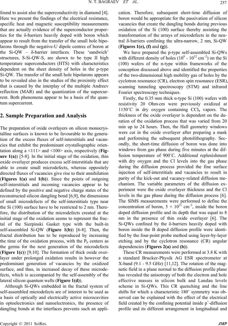 N. T. BAGRAEV ET AL. 257 found to assist also the superconductivity in diamond [4]. Here we present the findings of the electrical resistance, specific heat and magnetic susceptibility measurements that are actually evidence of the superconductor proper- ties for the δ-barriers heavily doped with boron which appear to result from the transfer of the small hole bipo- larons through the negative-U dipole centres of boron at the Si-QW – δ-barrier interfaces. These ‘sandwich’ structures, S-Si-QW-S, are shown to be type II high temperature superconductors (HTS) with characteristics dependent on the sheet density of holes in the p-type Si-QW. The transfer of the small hole bipolarons appears to be revealed also in the studies of the proximity effect that is caused by the interplay of the multiple Andreev reflection (MAR) and the quantization of the supercur- rent. Both phenomena appear to be a basis of the quan- tum supercurrent. 2. Sample Preparation and Analysis The preparation of oxide overlayers on silicon monocrys- talline surfaces is known to be favourable to the genera- tion of the excess fluxes of self-interstitials and vacan- cies that exhibit the predominant crystallographic orien- tation along a <111> and <100> axis, respectively (Fig- ure 1(a)) [5-8]. In the initial stage of the oxidation, thin oxide overlayer produces excess self-interstitials that are able to create small microdefects, whereas oppositely directed fluxes of vacancies give rise to their annihilation (Figures 1(a) and 1(b)). Since the points of outgoing self-interstitials and incoming vacancies appear to be defined by the positive and negative charge states of the reconstructed silicon d anglin g bond [6,9], the dimensions of small microdefects of the self-interstitials type near the Si (100) surface have to be restricted to 2 nm. There- fore, the distribution of the microdefects created at the initial stage of the oxidation seems to represent the frac- tal of the Sierpinski Gasket type with the built-in self-assembled Si-QW (Figure 1(b)) [6-8]. Then, the fractal distribution has to be reproduced by increasing the time of the oxidation process, with the Pb centers as the germs for the next generation of the microdefects (Figure 1(c)) [9,10]. The formation of thick oxide over- layer under prolonged oxidation results in however the predominant generation of vacancies by the oxidized surface, and thus, in increased decay of these microde- fects, which is accompanied by the self-assembly of the lateral silicon quantum wells (Figure 1(d)). Although Si-QWs embedded in the fractal system of self-assembled microdefects are of interest to be used as a basis of optically and electrically active microcavities in optoelectronics and nanoelectronics, the presence of dangling bonds at the interfaces prevents such an appli- cation. Therefore, subsequent short-time diffusion of boron would be approp riate for the passivation o f silicon vacancies that create the dangling bonds during previous oxidation of the Si (100) surface thereby assisting the transformation of the arrays of microdefects in the neu- tral -barriers confining the ultra-narrow, 2 nm, Si-QW (Figures 1(e), (f ) and (g)). We have prepared the p-type self-assembled Si-QWs with different density of holes (109 - 1012 cm–2) on the Si (100) wafers of the n-type within frameworks of the conception discussed above and identified the properties of the two-dimensional high mobility gas of holes by the cyclotron resonance (CR), electron spin resonance (ESR), scanning tunneling spectroscopy (STM) and infrared Fourier spectroscopy techniques. Firstly, the 0.35 mm thick n-type Si (100) wafers with resistivity 20 Ohmcm were previously oxidized at 1150˚C in dry oxygen containing CCl4 vapors. The thickness of the oxide overlayer is dependent on the du- ration of the oxidation process that was varied from 20 min up to 24 hours. Then, the Hall geometry windows were cut in the oxide overlayer after preparing a mask and performing the subsequent photolithography. Sec- ondly, the short-time diffusion of boron was done into windows from gas phase during five minutes at the dif- fusion temperature of 900˚C. Additional replenishment with dry oxygen and the Cl levels into the gas phase during the diffusion process provided the fine surface injection of self-interstitials and vacancies to result in parity of the kick-out and vacancy-related diffusion me- chanism. The variable parameters of the diffusion ex- periment were the oxide overlayer thickness and the Cl levels in the gas phase during the diffusion process [6]. The SIMS measurements were performed to define the concentration of boron, 5 × 1021 cm–3, inside the boron doped diffusion profile and its depth that was equal to 8 nm in the presence of thin oxide overlayer [6]. The Si-QWs confined by the δ-barriers heavily doped with boron inside the B doped diffusion profile were identi- fied by the four-point probe method using layer-by-layer etching and by the cyclotron resonance (CR) angular dependencies (Figures 2(a) and (b)). These CR measurements were performed at 3.8 K with a standard Brucker-Physik AG ESR spectrometer at X-band (9.1 - 9.5 GHz) [11,12]. The rotation of the mag- netic field in a plane normal to the diffusion profile plane has revealed the anisotropy of both the electron and hole effective masses in silicon bulk and Landau levels scheme in Si-QWs. This CR quenching and the line shifts for which a characteristic 180˚ symmetry was ob- served can be explained with the effect of the electrical field created b y the confinin g potential insid e p+-diffusion profile and its different arranement in longitudinal and g Copyright © 2011 SciRes. JMP 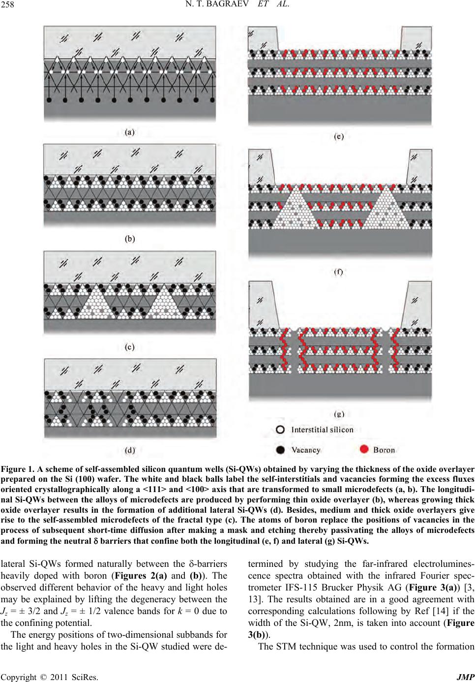 N. T. BAGRAEV ET AL. Copyright © 2011 SciRes. JMP 258 Figure 1. A scheme of self-assembled silicon quantum wells (Si-QWs) obtained by varying the thickness of the oxide overlayer prepared on the Si (100) wafer. The white and black balls label the self-interstitials and vacancies forming the excess fluxes oriented crystallographically along a <111> and <100> axis that are transformed to small microdefects (a, b). The longitudi- nal Si-QWs between the alloys of microdef ects are produced by performing thin oxide overlayer (b), whereas growing thick oxide overlayer results in the formation of additional lateral Si-QWs (d). Besides, medium and thick oxide overlayers give rise to the self-assembled microdefects of the fractal type (c). The atoms of boron replace the positions of vacancies in the process of subsequent short-time diffusion after making a mask and etching thereby passivating the alloys of microdefects and forming the neutral barriers that confine both the longitudinal (e, f) and lateral (g) Si-QWs. lateral Si-QWs formed naturally between the -barriers heavily doped with boron (Figures 2(a) and (b)). The observed different behavior of the heavy and light holes may be explained by lifting the degeneracy between the Jz = ± 3/2 and Jz = ± 1/2 valence bands for k = 0 due to the confining potential. The energy positions of two-dimensional subbands for the light and heavy holes in the Si-QW studied were de- termined by studying the far-infrared electrolumines- cence spectra obtained with the infrared Fourier spec- trometer IFS-115 Brucker Physik AG (Figure 3(a)) [3, 13]. The results obtained are in a good agreement with corresponding calculations following by Ref [14] if the width of the Si-QW, 2nm, is taken into account (Figure 3(b)). The STM technique was usd to control the formation e  N. T. BAGRAEV ET AL. 259 (a) (b) Figure 2. Cyclotron resonance spectra for the ultra-shallow boron diffusion profiles obtained on the n-type silicon {100} sur- faces at the diffusion temperatures of 900˚C (a) and 1100˚C (b) which consist of the -barriers confining the longitudinal (a) and lateral (b) Si-QW. Rotation of magnetic field B in a {110}-plane perpendicular to a {100}-surface of profiles (0˚ = B surface; 90˚ = B su rface), T = 3.8 K, = 9.45 GHz Figure 3. Electroluminescence spectrum (a) that defines the energies of two-dimensional subbands of heavy and light holes in the p-type Si-QW confined by the - barriers heavily doped with boron on the n-type Si (100) surface (b). T = 300 K (c) Transmission spectrum that reveals both the local phonon mode, = 16.4 m, and the superconductor gap, = 26.9 m, manifestation. (d) The reflection spectra from the n-type Si (100) surface and from the ultra-shallow boron diffusion profiles prepared on the n-type Si (100) surface that consist of the -barriers confining the ultra-narrow Si-QW. The curves 1-4 are related to the - barriers with different concentration of boron. The values of the concentration boron in different samples are characterized by the following ratio: curve 1 – 0.2, 2 – 0.3, 3 – 0.35, 4 – 0.4. The concentration of boron in the sample haracterized by the fourth curve is equal to 5 × 1021 cm-3. T = 300 K. c Copyright © 2011 SciRes. JMP 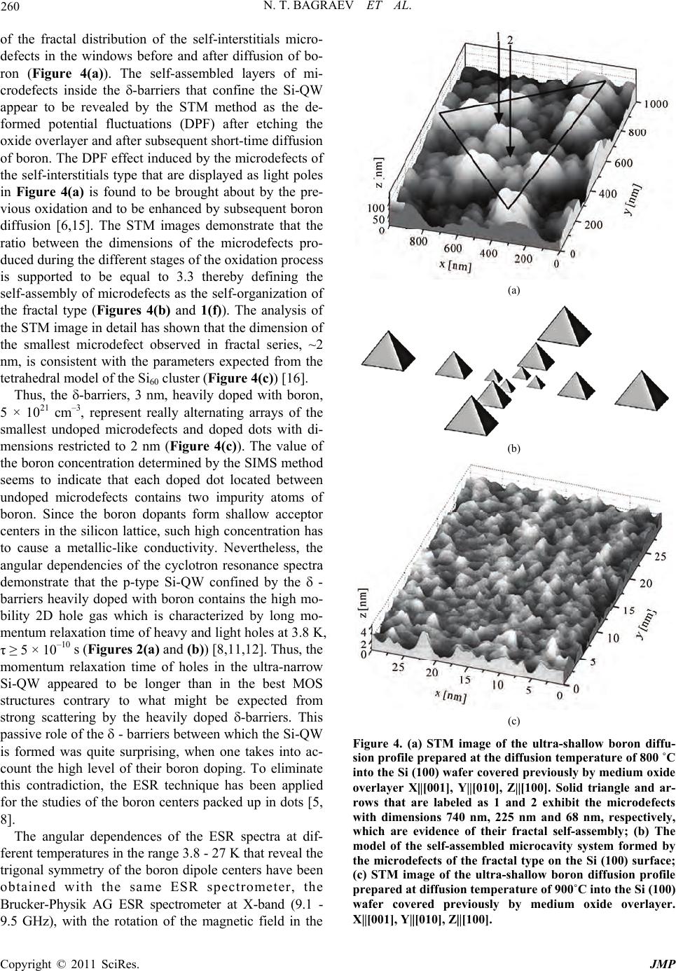 N. T. BAGRAEV ET AL. Copyright © 2011 SciRes. JMP 260 of the fractal distribution of the self-interstitials micro- defects in the windows before and after diffusion of bo- ron (Figure 4(a)). The self-assembled layers of mi- crodefects inside the -barriers that confine the Si-QW appear to be revealed by the STM method as the de- formed potential fluctuations (DPF) after etching the oxide overlayer an d after subsequen t short-time diffu sion of boron. The DPF effect induced by the microdefects of the self-interstitials type that are displayed as light poles in Figure 4(a) is found to be brought about by the pre- vious oxidation and to be enhanced by subsequent boron diffusion [6,15]. The STM images demonstrate that the ratio between the dimensions of the microdefects pro- duced during the different stages of the oxidation process is supported to be equal to 3.3 thereby defining the self-assembly of microdefects as the self-organization of the fractal type (Figures 4(b) and 1(f)). The analysis of the STM image in detail has sh own that th e dimension of the smallest microdefect observed in fractal series, ~2 nm, is consistent with the parameters expected from the tetrahedral model of the Si60 cluster (Figure 4(c)) [16]. Thus, the -barriers, 3 nm, heavily doped with boron, 5 × 1021 cm–3, represent really alternating arrays of the smallest undoped microdefects and doped dots with di- mensions restricted to 2 nm (Figure 4(c)). The value of the boron concentration determined by the SIMS method seems to indicate that each doped dot located between undoped microdefects contains two impurity atoms of boron. Since the boron dopants form shallow acceptor centers in the silicon lattice, such high concentration has to cause a metallic-like conductivity. Nevertheless, the angular dependencies of the cyclotron resonance spectra demonstrate that the p-type Si-QW confined by the - barriers heavily doped with boron contains the high mo- bility 2D hole gas which is characterized by long mo- mentum relaxation time of heavy and light holes at 3.8 K, τ ≥ 5 × 10⁻¹⁰ s (Figures 2(a) and (b)) [8,11,12 ]. Thus, th e momentum relaxation time of holes in the ultra-narrow Si-QW appeared to be longer than in the best MOS structures contrary to what might be expected from strong scattering by the heavily doped -barriers. This passive role of the - barriers between which the Si-QW is formed was quite surprising, when one takes into ac- count the high level of their boron doping. To eliminate this contradiction, the ESR technique has been applied for the studies of the boron centers packed up in dots [5, 8]. The angular dependences of the ESR spectra at dif- ferent temperatures in the range 3.8 - 27 K that reveal the trigonal symmetry of the boron dipole centers have been obtained with the same ESR spectrometer, the Brucker-Physik AG ESR spectrometer at X-band (9.1 - 9.5 GHz), with the rotation of the magnetic field in the (a) (b) (c) Figure 4. (a) STM image of the ultra-shallow boron diffu- sion profile prepared at the diffusion temperature of 800 ˚C into the Si (100) wafer covered previously by medium oxide overlayer X[001], Y[010], Z[100]. Solid triangle and ar- rows that are labeled as 1 and 2 exhibit the microdefects with dimensions 740 nm, 225 nm and 68 nm, respectively, which are evidence of their fractal self-assembly; (b) The model of the self-assembled microcavity system formed by the microdefects of the fractal type on the Si (100) surface; (c) STM image of the ultra-shallow boron diffusion profile prepared at diffusion temperature of 900˚C into the Si (100) wafer covered previously by medium oxide overlayer. X[001], Y[010], Z[100]. 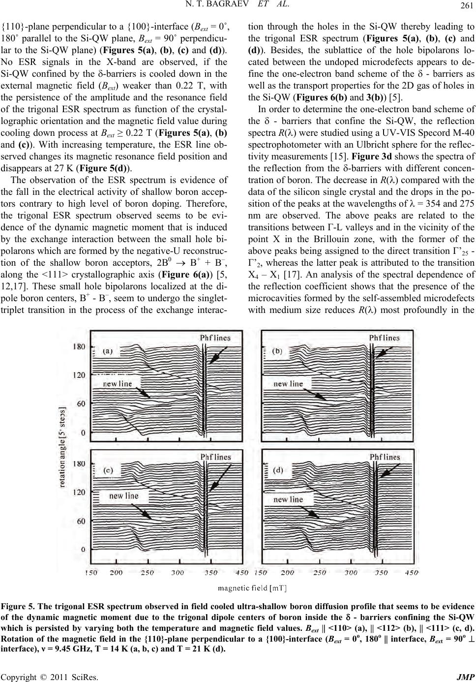 N. T. BAGRAEV ET AL. 261 {110}-plane perpendicular to a {100}-interface (Bext = 0˚, 180˚ parallel to the Si-QW plane, Bext = 90˚ perpendicu- lar to the Si-QW plane) (Figures 5(a), (b), (c) and (d)). No ESR signals in the X-band are observed, if the Si-QW confined by the -barriers is cooled down in the external magnetic field (Bext) weaker than 0.22 T, with the persistence of the amplitude and the resonance field of the trigonal ESR spectrum as function of the crystal- lographic orientation and the magnetic field value during cooling down process at Bext ≥ 0.22 T (Figures 5(a), (b) and (c)). With increasing temperature, the ESR line ob- served changes its magnetic resonance field position and disappears at 27 K (Figure 5(d)). The observation of the ESR spectrum is evidence of the fall in the electrical activity of shallow boron accep- tors contrary to high level of boron doping. Therefore, the trigonal ESR spectrum observed seems to be evi- dence of the dynamic magnetic moment that is induced by the exchange interaction between the small hole bi- polarons which are formed by the negative-U reconstruc- tion of the shallow boron acceptors, 2B0 B + + B–, along the <111> crystallographic axis (Figure 6(a)) [5, 12,17]. These small hole bipolarons localized at the di- pole boron centers, B+ - B–, seem to undergo the singlet- triplet transition in the process of the exchange interac- tion through the holes in the Si-QW thereby leading to the trigonal ESR spectrum (Figures 5(a), (b), (c) and (d)). Besides, the sublattice of the hole bipolarons lo- cated between the undoped microdefects appears to de- fine the one-electron band scheme of the - barriers as well as the transport properties for the 2D gas of holes in the Si-QW (Figures 6(b) and 3(b)) [5]. In order to determine the one-electron band scheme of the - barriers that confine the Si-QW, the reflection spectra R() were studied using a UV-VIS Specord M-40 spectrophotometer with an Ulbricht sphere for the reflec- tivity measurements [15]. Figure 3d shows the spectra of the reflection from the -barriers with different concen- tration of boron. The decrease in R() compared with the data of the silicon single crystal and the drops in the po- sition of the peaks at the wavelengths of = 354 and 275 nm are observed. The above peaks are related to the transitions between Γ-L valleys and in th e vicinity of the point X in the Brillouin zone, with the former of the above peaks being assigned to the direct transition Γ’25 - Γ’2, whereas the latter peak is attributed to the transition X4 – X1 [17]. An analysis of the spectral dependence of the reflection coefficient shows that the presence of the microcavities formed by the self-assembled microdefects with medium size reduces R() most profoundly in the Figure 5. The trigonal ESR spectrum observed in field cooled ultra-shallow boron diffusion profile that seems to be evidence of the dynamic magnetic moment due to the trigonal dipole centers of boron inside the - barriers confining the Si-QW which is persisted by varying both the temperature and magnetic field values. Bext <110> (a), <112> (b), <111> (c, d). Rotation of the magnetic field in the {110}-plane perpendicular to a {100}-interface (Bext = 0o, 180o interface, Bext = 90o interface), ν = 9.45 GHz, T = 14 K (a, b, c) and T = 21 K (d). Copyright © 2011 SciRes. JMP 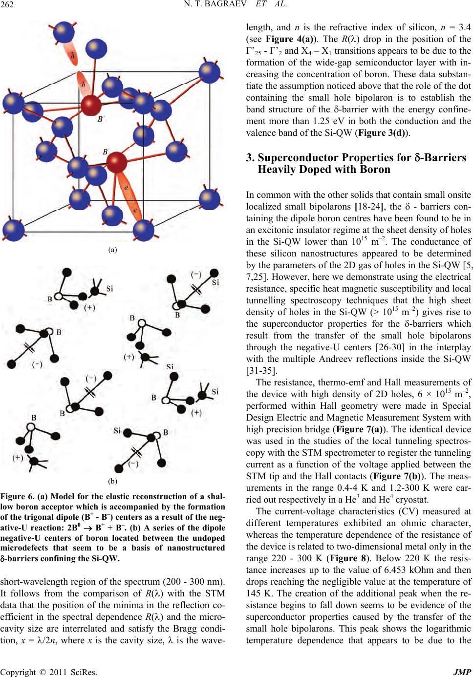 N. T. BAGRAEV ET AL. Copyright © 2011 SciRes. JMP 262 (a) (b) Figure 6. (a) Model for the elastic reconstruction of a shal- low boron acceptor which is accompanied by the formation of the trigonal dipole (B+ - B–) centers as a result of the neg- ative-U reaction: 2B0 B+ + B–. (b) A series of the dipole negative-U centers of boron located between the undoped microdefects that seem to be a basis of nanostructured -barriers confining the Si-QW. short-waveleng th region of the spectrum (200 - 300 nm). It follows from the comparison of R() with the STM data that the position of the minima in the reflection co- efficient in the spectral dependence R() and the micro- cavity size are interrelated and satisfy the Bragg condi- tion, x = /2n, where x is the cavity size, is the wave- length, and n is the refractive index of silicon, n = 3.4 (see Figure 4(a)). The R() drop in the position of the Γ’25 - Γ’2 and X4 – X1 transitions appears to be due to the formation of the wide-gap semiconductor layer with in- creasing the concentration of boron. These data substan- tiate the assumption no ticed ab ove th at the role of th e dot containing the small hole bipolaron is to establish the band structure of the -barrier with the energy confine- ment more than 1.25 eV in both the conduction and the valence band of the Si-QW (Figure 3(d) ). 3. Superconductor Properties for -Barriers Heavily Doped with Boron In common with the other solid s th at con tain small onsite localized small bipolarons [18-24], the - barriers con- taining the dipole bo ron centres have b een found to be in an excitonic insulator regime at the sheet density of holes in the Si-QW lower than 1015 m–2. The conductance of these silicon nanostructures appeared to be determined by the parameters of the 2D gas of holes in the Si-QW [5, 7,25]. However, here we demonstrate using the electrical resistance, specific heat magnetic suscep tibility and local tunnelling spectroscopy techniques that the high sheet density of holes in the Si-QW (> 1015 m–2) gives rise to the superconductor properties for the -barriers which result from the transfer of the small hole bipolarons through the negative-U centers [26-30] in the interplay with the multiple Andreev reflections inside the Si-QW [31-35]. The resistance, thermo-emf and Hall measurements of the device with high density of 2D holes, 6 × 10¹⁵ m–2, performed within Hall geometry were made in Special Design Electric and Magnetic Measurement System with high precision bridge (Figure 7(a)). The identical device was used in the studies of the local tunneling spectros- copy with the STM spectro meter to register th e tunn eling current as a function of the voltage applied between the STM tip and the Hall contacts (Figure 7(b)). The meas- urements in the range 0.4-4 K and 1.2-300 K were car- ried out respectively in a He3 and He4 cryostat. The current-voltage characteristics (CV) measured at different temperatures exhibited an ohmic character, whereas the temperature dependence of the resistance of the device is related to two -dimen sio nal metal o n ly in th e range 220 - 300 K (Figure 8). Below 220 K the resis- tance increases up to the value of 6.453 kOhm and then drops reaching the negligible value at the temperature of 145 K. The creation of the additional peak when the re- sistance begins to fall down seems to be evidence of the superconductor properties caused by the transfer of the small hole bipolarons. This peak shows the logarithmic temperature dependence that appears to be due to the  N. T. BAGRAEV ET AL. 263 (a) (b) Figure 7. (a) Schematic diagram of the devices that demon- strates a perspective view of the p-type Si-QW confined by the - barriers heavily doped with boron on the n-type Si (100) surface. The top gate is able to control the sheet den- sity of holes and the Rashba SOI value. The depletion re- gions indicate the Hall geometry of leads; (b) Planar field- effect silicon transistor structure with the STM tip, which is based on an ultra-shallow p+-diffusion profile prepared in the Hall geometry. The circle dashed line exhibits the point STM contact region. Figure 8. The resistance temperature dependences that were observed in the ultra-shallow p+-diffusion profile which contains the p-type Si-QW confined by the δ - barriers heavily doped with boro n on the n-type Si (100) surface. Kondo-liked scattering of the single 2D holes tunneling through the negative-U boron dipole centres of boron at the Si-QW – - barrier interfaces. As was to be expected, the application of external magnetic field results in the shift of the resistance drop to lower temperatures, which is accompanied by the weak broadening of the transition and the conservation of the peak values of the resistance (Figure 8). Similar peaks followed by the drops of the resistance revealed in its temperature dependences are evidence of the Kondo-liked scattering that seems to be the precursor of the optimal tunneling of single holes into the negative-U boron cen- ters of boron [36]. This process is related to the conduc- tion electron tunneling into the negativ e-U centers that is favourable to the increase of the superconducting transi- tion temperature, Tc, in metal-silicon eutectic alloys [26, 27]. The effect of single-hole tunneling is also possible to resolve some bottlenecks in the bipolaronic mecha- nism of the high temperature superconductivity, which results from the distance between the negative-U centers lesser than the coherence length [28,30]. Besides, two experimental facts are needed to be noticed. Firstly, the maximum value of th e resistan ce, 6.45 3 kOhm h/4e2, is independent of the external magnetic field. Secondly, applying a magnetic field is surprised to stabilize the - barrier in the state of the two-dimensional metal u p to th e temperature value corresponding to the shift of a transi- tion to lower temperatures (Figure 8). Thus, the -barri- ers confining Si-QW seem to be self-organized as gra- phene [37] owing to heavily doping with boron which gives rise to the formation of the negative-U dipole cen- ters. The value of the critical temperature, Tc = 145 K, the estimations of the superconductor gap, 2 = 0.044 eV, Copyright © 2011 SciRes. JMP 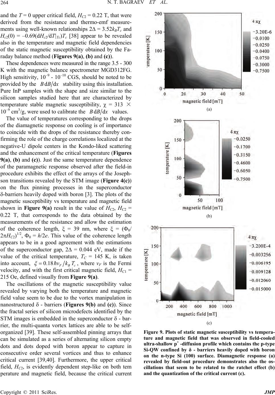 264 N. T. BAGRAEV ET AL. and the T = 0 upper critical field, HC2 = 0.22 T, that were derived from the resistance and thermo-emf measure- ments using well-known relationships 2 = 3.52kBTc and Hc2(0) = –0.69(dHc2/dT|Tc)Tc [38] appear to be revealed also in the temperature and magnetic field dependencies of the static magnetic susceptibility obtained by the Fa- raday balan ce metho d (Figures 9(a), (b) and (c)). These dependences w ere measured in the range 3.5 - 300 K with the magnetic balance spectrometer MGD312FG. High sensitivity, 10–9 - 10–10 CGS, should be no ted to be provided by the ddBB x stability us ing th is installation . Pure InP samples with the shape and size similar to the silicon samples studied here that are characterized by temperature stable magnetic susceptibility, = 313 × 10–9 cm3/g, were used to calibrate the ddBB x values. The value of temperatures corresponding to the drops of the diamagnetic response on cooling is of importance to coincide with the drops of the resistance thereby con- firming the role of the charge correlations localized at the negative-U dipole centers in the Kondo-liked scattering and the enhancement of the critical temperature (Figures 9(a), (b) and (c)). Just the same temperature dependence of the paramagnetic response observed after the field-in procedure exhibits the effect of the arrays of the Joseph- son transitions revealed by the STM image ( Figure 4(c)) on the flux pinning processes in the superconductor -barriers heavily doped with boron [3]. The plots of the magnetic susceptibility vs temperature and magnetic field shown in Figure 9(a) result in the value of HC2, HC2 = 0.22 T, that corresponds to the data obtained by the measurements of the resistance and allow the estimation of the coherence length, ξ = 39 nm, where ξ = (0/ 2HC2)1/2, 0 = h/2e. This value of the coherence length appears to be in a good agreement with the estimations of the superconductor gap, 2 = 0.044 eV, made if the value of the critical temperature, TC = 145 K, is taken into account, 0.18 Bc vkT , where vF is the Fermi velocity, and with the first critical magnetic field, HC1 = 215 Oe, defi ned visuall y fr om Figure 9(a). The oscillations of the magnetic susceptibility value revealed by varying both the temperature and magnetic field value seem to be due to the vortex manipulation in nanostructured - barriers (Figures 9(b) and (c)). Since the fractal series of silicon microdefects identified b y the STM images is embedded in the superconductor - bar- rier, the multi-quanta vortex lattices are able to be self- organized [39]. These self-assembled pinning arrays that can be simulated as a series of alternating silicon empty dots and dots doped with boron appear to capture in consecutive order several vortices and thus to enhance critical current [39,40]. Furthermore, the upper critical field, HC2, is evidently dependent step-like on both tem perature and magnetic field, because the critical current (a) (b) (c) Figure 9. Plots of static magnetic susceptibility vs tempera- ture and magnetic field that was observed in field-cooled ultra-shallow p+ -diffusion profile which contains the p-type Si-QW confined by δ - barriers heavily doped with boron on the n-type Si (100) surface. Diamagnetic response (a) revealed by field-out procedure demonstrates also the os- cillations that seem to be related to the ratchet effect (b) and the quantization of the critical current (c). Copyright © 2011 SciRes. JMP 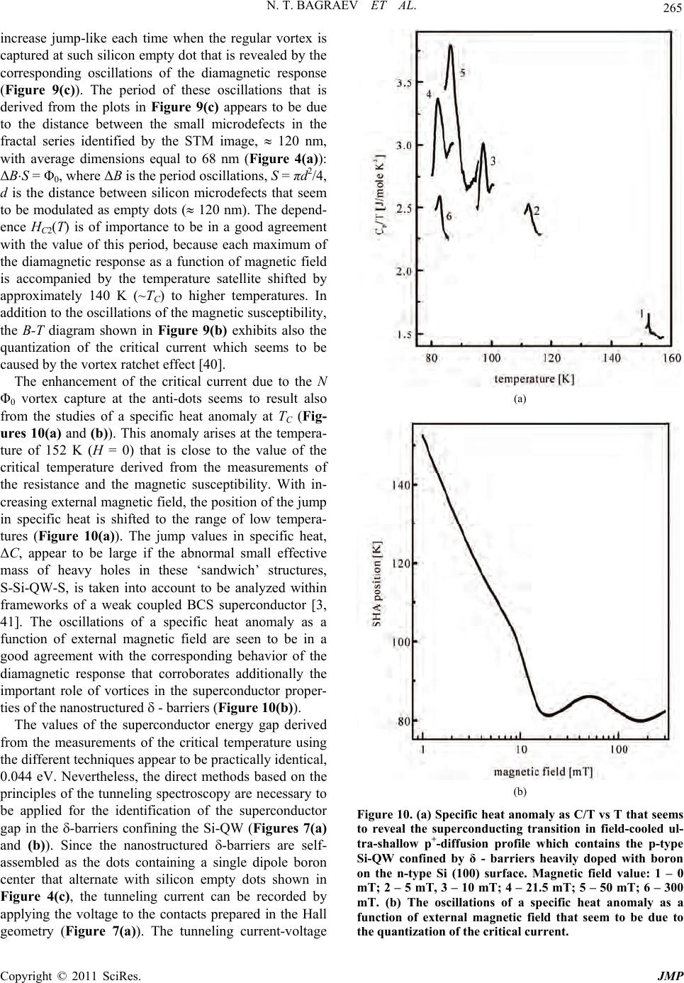 N. T. BAGRAEV ET AL. 265 increase jump-like each time when the regular vortex is captured at such silico n empty dot that is revealed by the corresponding oscillations of the diamagnetic response (Figure 9(c)). The period of these oscillations that is derived from the plots in Figure 9(c) appears to be due to the distance between the small microdefects in the fractal series identified by the STM image, 120 nm, with average dimensions equal to 68 nm (Figure 4(a)): ΔBS = Φ0, where ΔB is the period oscillations, S = πd2/4, d is the distance between silicon microdefects that seem to be modulated as empty dots ( 120 nm). The depend- ence HC2(T) is of importance to be in a good agreement with the value of this period, because each maximum of the diamagnetic response as a function of magnetic field is accompanied by the temperature satellite shifted by approximately 140 K (~TC) to higher temperatures. In addition to the oscillatio ns of the magnetic susceptib ility, the B-T diagram shown in Figure 9(b) exhibits also the quantization of the critical current which seems to be caused by the vortex ratchet effect [40]. The enhancement of the critical current due to the N Φ0 vortex capture at the anti-dots seems to result also from the studies of a specific heat anomaly at TC (Fig- ures 10(a) and (b)). This anomaly arises at the tempera- ture of 152 K (H = 0) that is close to the value of the critical temperature derived from the measurements of the resistance and the magnetic susceptibility. With in- creasing external magnetic field, the position of the jump in specific heat is shifted to the range of low tempera- tures (Figure 10(a)). The jump values in specific heat, ΔC, appear to be large if the abnormal small effective mass of heavy holes in these ‘sandwich’ structures, S-Si-QW-S, is taken into account to be analyzed within frameworks of a weak coupled BCS superconductor [3, 41]. The oscillations of a specific heat anomaly as a function of external magnetic field are seen to be in a good agreement with the corresponding behavior of the diamagnetic response that corroborates additionally the important role of vortices in the superconductor proper- ties of the nanostructured - barriers (Figure 10(b)). The values of the superconductor energy gap derived from the measurements of the critical temperature using the different techniques appear to be practically identical, 0.044 eV. Nevertheless, the direct methods based on the principles of the tunneling spectroscopy are necessary to be applied for the identification of the superconductor gap in the -barriers confining the Si-QW (Figures 7(a) and (b)). Since the nanostructured -barriers are self- assembled as the dots containing a single dipole boron center that alternate with silicon empty dots shown in Figure 4(c), the tunneling current can be recorded by applying the voltage to the contacts prepared in the Hall geometry (Figure 7(a)). The tunneling current-voltage (a) (b) Figure 10. (a) Specific heat anomaly as C/T vs T that seems to reveal the superconducting transition in field-cooled ul- tra-shallow p+-diffusion profile which contains the p-type Si-QW confined by δ - barriers heavily doped with boron on the n-type Si (100) surface. Magnetic field value: 1 – 0 mT; 2 – 5 mT, 3 – 10 mT; 4 – 21.5 mT; 5 – 50 mT; 6 – 300 mT. (b) The oscillations of a specific heat anomaly as a function of external magnetic field that seem to be due to the quantization of the critical current. Copyright © 2011 SciRes. JMP 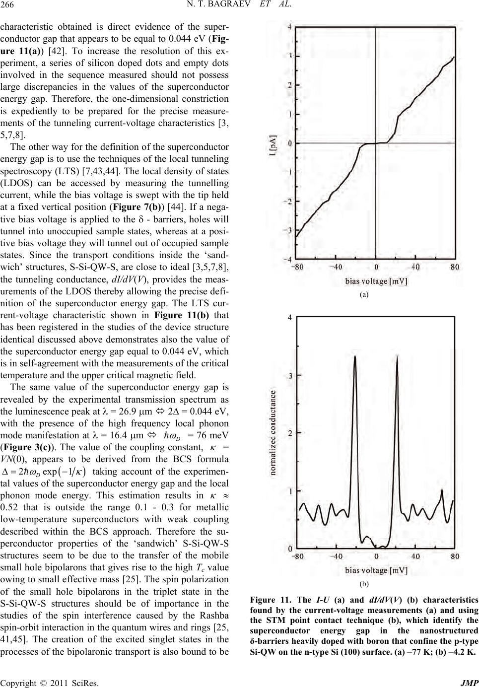 266 N. T. BAGRAEV ET AL. characteristic obtained is direct evidence of the super- conductor gap that appears to be equal to 0.044 eV (Fig- ure 11(a)) [42]. To increase the resolution of this ex- periment, a series of silicon doped dots and empty dots involved in the sequence measured should not possess large discrepancies in the values of the superconductor energy gap. Therefore, the one-dimensional constriction is expediently to be prepared for the precise measure- ments of the tunneling current-voltage characteristics [3, 5,7,8]. The other way for the definition of the superconductor energy gap is to use the techniques of the local tunneling spectroscopy (LTS) [7,43,44]. The local density of states (LDOS) can be accessed by measuring the tunnelling current, while the bias voltage is swept with the tip held at a fixed vertical position (Figure 7(b)) [44]. If a nega- tive bias voltage is applied to the - barriers, holes will tunnel into unoccupied sample states, whereas at a posi- tive bias voltage th ey will tunnel out of occupied sample states. Since the transport conditions inside the ‘sand- wich’ structures, S-Si-QW-S, are close to ideal [3,5,7,8], the tunneling conductance, dI/dV(V), provides the meas- urements of the LDOS thereby allowing the precise defi- nition of the superconductor energy gap. The LTS cur- rent-voltage characteristic shown in Figure 11(b) that has been registered in the studies of the device structure identical discussed above demonstrates also the value of the superconductor energy gap equal to 0.044 eV, which is in self-agreement with the measurements of the critical temperature and the upper critical magnetic field. The same value of the superconductor energy gap is revealed by the experimental transmission spectrum as the luminescence peak at = 26.9 m 2 = 0.044 eV, with the presence of the high frequency local phonon mode manifestation at = 16.4 m = 76 meV (Figure 3(c)). The value of the coupling constant, = VN(0), appears to be derived from the BCS formula 2exp1 D (a) taking account of the experimen- tal values of the superconductor energy gap and the local phonon mode energy. This estimation results in 0.52 that is outside the range 0.1 - 0.3 for metallic low-temperature superconductors with weak coupling described within the BCS approach. Therefore the su- perconductor properties of the ‘sandwich’ S-Si-QW-S structures seem to be due to the transfer of the mobile small hole bipolarons that gives rise to the high Tc value owing to small effective mass [25]. The spin polarization of the small hole bipolarons in the triplet state in the S-Si-QW-S structures should be of importance in the studies of the spin interference caused by the Rashba spin-orbit interaction in the quantum wires and rings [25, 41,45]. The creation of the excited singlet states in the processes of the bipolaronic transport is also bound to be (b) Figure 11. The I-U (a) and dI/dV(V) (b) characteristics found by the current-voltage measurements (a) and using the STM point contact technique (b), which identify the superconductor energy gap in the nanostructured δ-barriers heavily dope d with boron that confine the p-type Si-QW on the n-type Si (100) surface. (a) –77 K; (b) –4.2 K. Copyright © 2011 SciRes. JMP 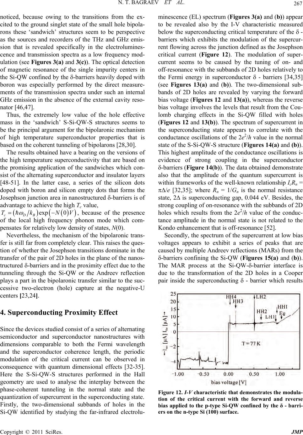 N. T. BAGRAEV ET AL. 267 noticed, because owing to the transitions from the ex- cited to the ground singlet state of the small hole bipola- rons these ‘sandwich’ structures seem to be perspective as the sources and recorders of the THz and GHz emis- sion that is revealed specifically in the electrolumines- cence and transmission spectra as a low frequency mod- ulation (see Figures 3(a) and 3( c)). The optical detection of magnetic resonance of the single impurity centers in the Si-QW confined b y the -barriers heavily doped with boron was especially performed by the direct measure- ments of the transmission spectra under such an internal GHz emission in the absence of the external cavity reso- nator [46,47]. Thus, the extremely low value of the hole effective mass in the ‘sandwich’ S-Si-QW-S structures seems to be the principal argument for the bipolaronic mechanis m of high temperature superconductor properties that is based on the coherent tunneling of bipolarons [28,30]. The results obtained have a bearing on the versions of the high temperature superconductivity that are based on the promising application of the sandwiches which con- sist of the alternating sup erconductor and insulato r layers [48-51]. In the latter case, a series of the silicon dots doped with boron and silicon empty dots that forms the Josephson junction area in nanostructured -barriers is of advantage to achieve the high Tc value, exp 0 cDB TkN V, because of the presence of the local high frequency phonon mode which com- pensates for relatively low density of states, N(0). Nevertheless, the mechanism of the bipolaronic trans- fer is still far from completely clear. This raises the ques- tion of whether the Josephson tran sitions dominate in the transfer of the pair of 2D holes in the plane of the nanos- tructured -barriers and in the proximity effect due to the tunneling through the Si-QW or the Andreev reflection plays a part in the bipolaronic transfer similar to the suc- cessive two-electron (hole) capture at the negative-U centers [23,24]. 4. Superconducting Proximity Effect Since the devices studied consist of a series of alternating semiconductor and superconductor nanostructures with dimensions comparable to both the Fermi wavelength and the superconductor coherence length, the periodic modulation of the critical current can be observed in consequence with quantum dimensional effects [32-35]. Here the S-Si-QW-S structures performed in the Hall geometry are used to analyse the interplay between the phase-coherent tunneling in the normal state and the quantization of supercurrent in the superconducting state. Firstly, the two-dimensional subbands of holes in the Si-QW identified by studying the far-infrared electrolu- minescence (EL) spectrum (Figures 3(a) and (b) ) appear to be revealed also by the I-V characteristic measured below the superconducting critical temperature of the - barriers which exhibits the modulation of the supercur- rent flowing across the junction defined as the Josephson critical current (Figure 12). The modulation of super- current seems to be caused by the tuning of on- and off-resonance with the subbands of 2D holes relatively to the Fermi energy in superconductor - barriers [34,35] (see Figures 13(a) and (b)). The two-dimensional sub- bands of 2D holes are revealed by varying the forward bias voltage (Figures 12 and 13(a)), whereas the reverse bias voltage invo lves the levels that result fro m the Cou- lomb charging effects in the Si-QW filled with holes (Figures 12 and 13(b)). The spectrum of supercurrent in the superconducting state appears to correlate with the conductance oscillation s of the 2e2/h value in the normal state of the S-Si-QW-S structure (Figures 14(a) and (b)). This highest amplitude of the con ductance oscillations is evidence of strong coupling in the superconductor -barriers (Figure 14(b)). The data obtained demonstrate also that the amplitude of the quantum supercurrent is within frameworks of the well-known relationship IcRn = /e [32,35]; where Rn = 1/Gn is the normal resistance state, 2 is superconducting gap, 0.044 eV. Besides, the strong coupling of on-resonance with the subbands of 2D holes which results from the 2e2/h value of the conduc- tance amplitude in the normal state is not related to the Kondo enhancement that is off-resonance [52]. Secondly, the spectrum of the supercurrent at low bias voltages appears to exhibit a series of peaks that are caused by multiple Andreev reflection s (MARs) from the -barriers confining the Si-QW (Figures 15(a) and (b)). The MAR process at the Si-QW--barrier interface is due to the transformation of the 2D holes in a Cooper pair inside the superconducting - barrier which results Figure 12. I-V characteristic that demonstrates the modula- tion of the critical current with the forward and reverse bias applied to the p-type Si-QW confined by the δ - barri- ers on the n-type Si (100) surface. Copyright © 2011 SciRes. JMP 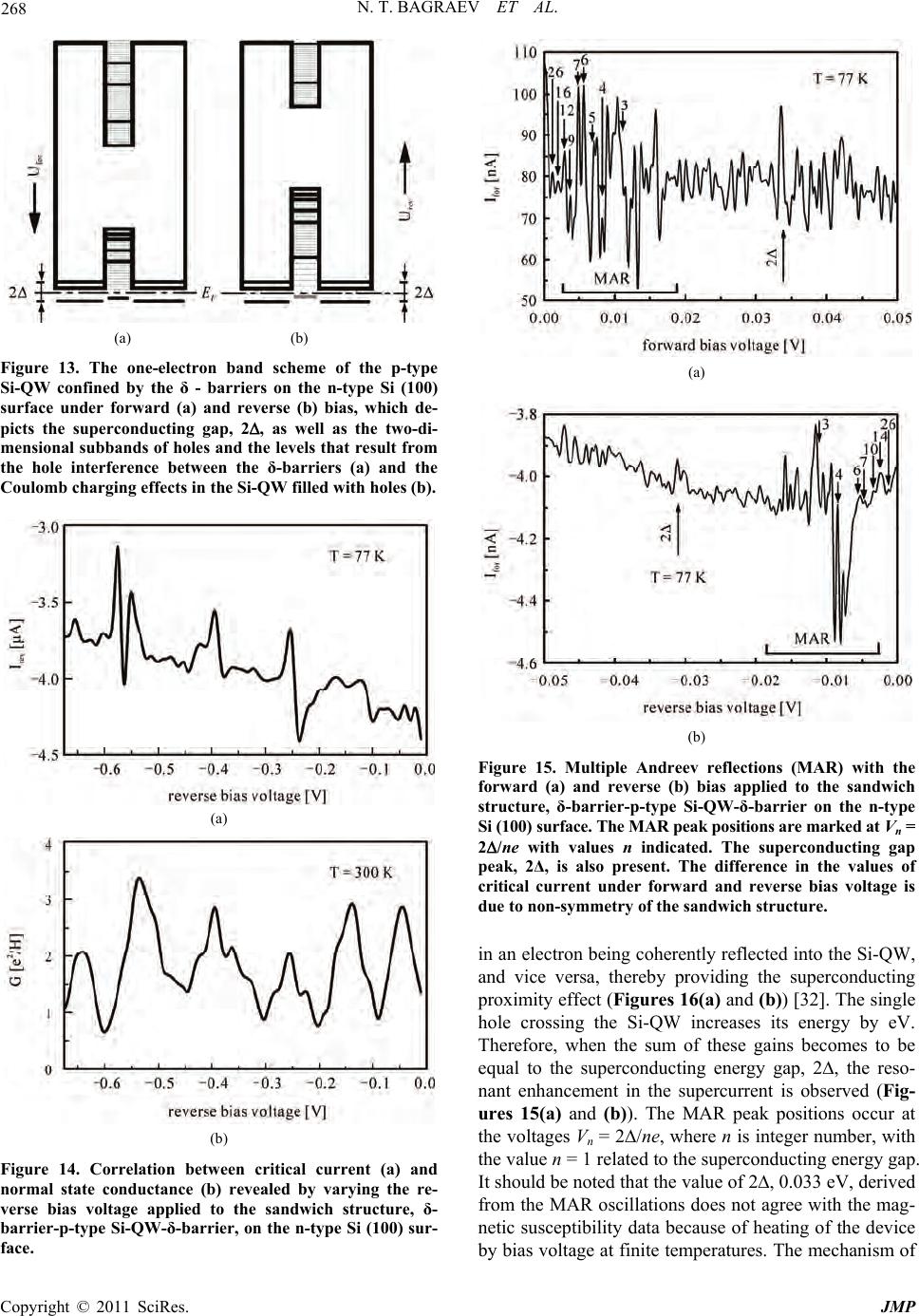 268 N. T. BAGRAEV ET AL. (a) (b) Figure 13. The one-electron band scheme of the p-type Si-QW confined by the δ - barriers on the n-type Si (100) surface under forward (a) and reverse (b) bias, which de- picts the superconducting gap, 2, as well as the two-di- mensional subbands of holes and the levels that result from the hole interference between the δ-barriers (a) and the Coulomb charging effects in the Si-QW filled with holes (b). (a) (b) Figure 14. Correlation between critical current (a) and normal state conductance (b) revealed by varying the re- verse bias voltage applied to the sandwich structure, δ- barrier-p-type Si-QW-δ-barrier, on the n-type Si (100) sur- face. (a) (b) Figure 15. Multiple Andreev reflections (MAR) with the forward (a) and reverse (b) bias applied to the sandwich structure, δ-barrier-p-type Si-QW-δ-barrier on the n-type Si (100) surface. The MAR peak positions are marked at Vn = 2/ne with values n indicated. The superconducting gap peak, 2Δ, is also present. The difference in the values of critical current under forward and reverse bias voltage is due to non-symmetry of the sandwich struct ur e. in an electron being coherently reflected into the Si-QW, and vice versa, thereby providing the superconducting proximity effect (Figures 16(a) and (b)) [32]. The single hole crossing the Si-QW increases its energy by eV. Therefore, when the sum of these gains becomes to be equal to the superconducting energy gap, 2, the reso- nant enhancement in the supercurrent is observed (Fig- ures 15(a) and (b)). The MAR peak positions occur at the voltages Vn = 2/ne, where n is integer number, with the value n = 1 related to the supercondu cting energ y gap. It should be noted that the value of 2, 0.033 eV, derived from the MAR oscillations does no t agree with the mag- netic susceptibility data because of heating of the device by bias voltage at finite temperatures. The mechanism of Copyright © 2011 SciRes. JMP 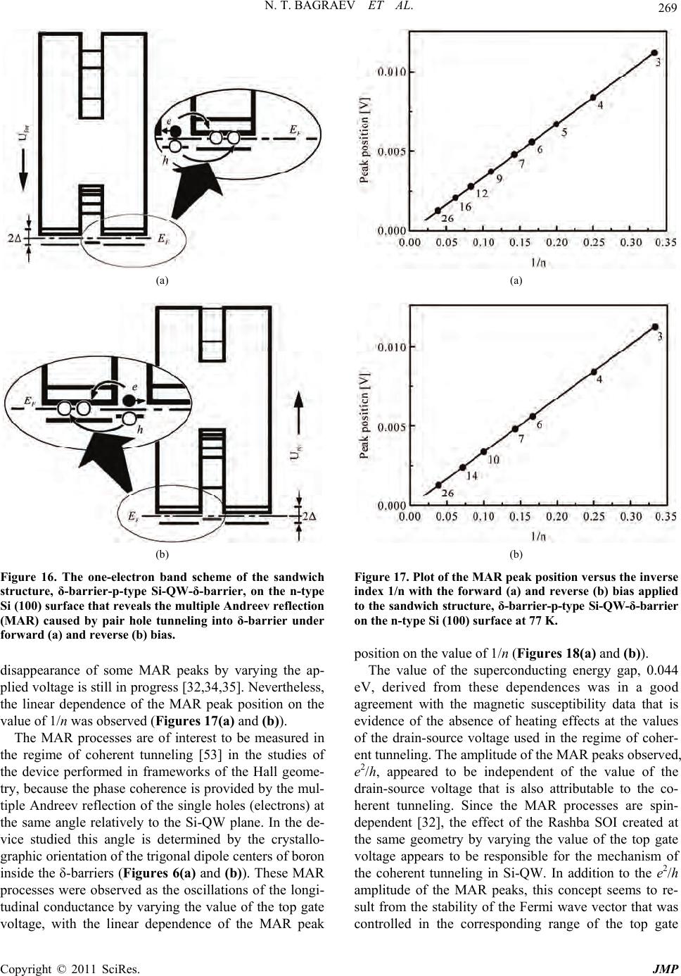 N. T. BAGRAEV ET AL. 269 (a) (b) Figure 16. The one-electron band scheme of the sandwich structure, δ-barrier-p-type Si-QW-δ-barrier, on the n-type Si (100) surface that reveals the multiple Andreev reflection (MAR) caused by pair hole tunneling into δ-barrier under forward (a) and reverse (b) bias. disappearance of some MAR peaks by varying the ap- plied voltage is still in progress [32,34 ,35]. Nevertheless, the linear dependence of the MAR peak position on the value of 1/n was observed (Figures 17(a) and (b)). The MAR processes are of interest to be measured in the regime of coherent tunneling [53] in the studies of the device performed in frameworks of the Hall geome- try, because the phase coherence is provided by the mul- tiple Andreev reflection of the single holes (electrons) at the same angle relatively to the Si-QW plane. In the de- vice studied this angle is determined by the crystallo- graphic orientation of the trigonal dipole centers of boron inside the δ-barriers (Figures 6(a) and (b)). These MAR processes were observed as the oscillations of the longi- tudinal conductance by varying the value of the top gate voltage, with the linear dependence of the MAR peak (a) (b) Figure 17. Plot of the MAR peak position versus the inverse index 1/n with the forward (a) and reverse (b) bias applied to the sandwich structure, δ-barrier-p-type Si-QW-δ-barrier on the n-type Si (100) surface at 77 K. position on the value of 1/n (Figures 18(a) and (b)). The value of the superconducting energy gap, 0.044 eV, derived from these dependences was in a good agreement with the magnetic susceptibility data that is evidence of the absence of heating effects at the values of the drain-source voltage used in the regime of coher- ent tunneling. The amplitude of the MAR peaks observed, e2/h, appeared to be independent of the value of the drain-source voltage that is also attributable to the co- herent tunneling. Since the MAR processes are spin- dependent [32], the effect of the Rashba SOI created at the same geometry by varying the value of the top gate voltage appears to be responsible for the mechanism of the coherent tunneling in Si-QW. In addition to the e2/h amplitude of the MAR peaks, this concept seems to re- sult from the stability of the Fermi wave vector that was controlled in the corresponding range of the top gate Copyright © 2011 SciRes. JMP 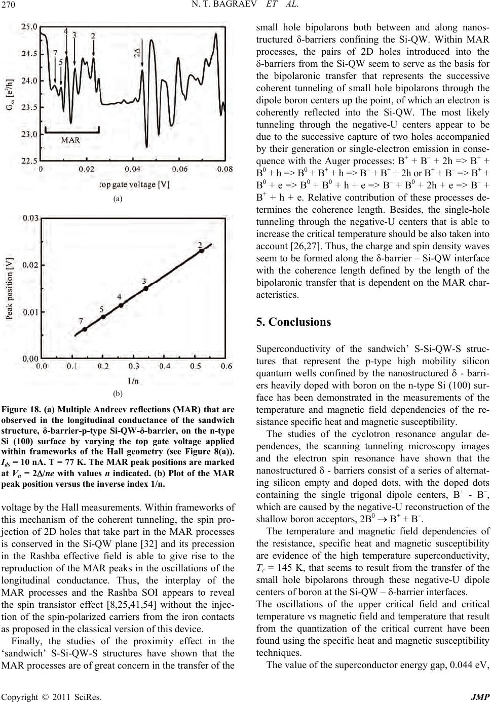 270 N. T. BAGRAEV ET AL. (a) (b) Figure 18. (a) Multiple Andreev reflections (MAR) that are observed in the longitudinal conductance of the sandwich structure, δ-barrier-p-type Si-QW-δ-barrier, on the n-type Si (100) surface by varying the top gate voltage applied within frameworks of the Hall geometry (see Figure 8(a)). Ids = 10 nA. T = 77 K. The MAR peak positions are marked at Vn = 2/ne with values n indicated. (b) Plot of the MAR peak position versus the inverse index 1/n. voltage by the Hall measurements. Within frameworks of this mechanism of the coherent tunneling, the spin pro- jection of 2D holes that take part in the MAR processes is conserved in the Si-QW plane [32] and its precession in the Rashba effective field is able to give rise to the reproduction of the MAR peaks in the oscillations of the longitudinal conductance. Thus, the interplay of the MAR processes and the Rashba SOI appears to reveal the spin transistor effect [8,25,41,54] without the injec- tion of the spin-polarized carriers from the iron contacts as proposed in the classical version of this device. Finally, the studies of the proximity effect in the ‘sandwich’ S-Si-QW-S structures have shown that the MAR processes are of great concern in the transfer of the small hole bipolarons both between and along nanos- tructured δ-barriers confining the Si-QW. Within MAR processes, the pairs of 2D holes introduced into the δ-barriers from the Si-QW seem to serve as the basis for the bipolaronic transfer that represents the successive coherent tunneling of small hole bipolarons through the dipole boron centers up the point, of which an electron is coherently reflected into the Si-QW. The most likely tunneling through the negative-U centers appear to be due to the successive capture of two holes accompanied by their generation or single-electron emission in conse- quence with the Auger processes: B+ + B– + 2h => B+ + B0 + h => B0 + B+ + h => B– + B+ + 2h or B+ + B– => B+ + B0 + e => B0 + B0 + h + e => B– + B0 + 2h + e => B– + B+ + h + e. Relative contribution of these processes de- termines the coherence length. Besides, the single-hole tunneling through the negative-U centers that is able to increase the critical temperature should be also taken into account [26,27]. Thus, the charge and spin density waves seem to be formed along the δ-barrier – Si-QW interface with the coherence length defined by the length of the bipolaronic transfer that is dependent on the MAR char- acteristics. 5. Conclusions Superconductivity of the sandwich’ S-Si-QW-S struc- tures that represent the p-type high mobility silicon quantum wells confined by the nanostructured - barri- ers heavily doped with boron on the n-type Si (100) sur- face has been demonstrated in the measurements of the temperature and magnetic field dependencies of the re- sistance specific heat and magnetic suscep tibility. The studies of the cyclotron resonance angular de- pendences, the scanning tunneling microscopy images and the electron spin resonance have shown that the nanostructured - barriers consist of a series o f alternat- ing silicon empty and doped dots, with the doped dots containing the single trigonal dipole centers, B+ - B–, which are caused by the negative-U reconstruction of the shallow boron acceptors, 2B 0 B+ + B–. The temperature and magnetic field dependencies of the resistance, specific heat and magnetic susceptibility are evidence of the high temperature superconductivity, Tc = 145 K, that seems to result from the transfer of the small hole bipolarons through these negative-U dipole centers of boron at the Si-QW – -barrier interfaces. The oscillations of the upper critical field and critical temperature vs magnetic field and temperature that result from the quantization of the critical current have been found using the specific heat and magnetic su sceptibility techniques. The value of the superconductor energy gap, 0.044 eV, Copyright © 2011 SciRes. JMP 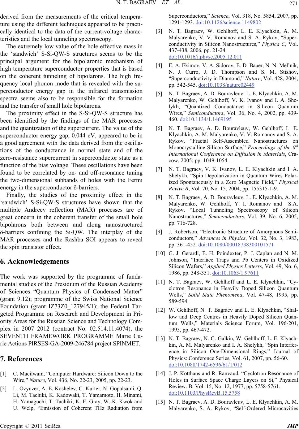 N. T. BAGRAEV ET AL. 271 derived from the measurements of the critical tempera- ture using the different techniques appeared to be practi- cally identical to the data of the current-voltage charac- teristics and the local tunneling spectroscopy. The extremely low value of the hole effective mass in the ‘sandwich’ S-Si-QW-S structures seems to be the principal argument for the bipolaronic mechanism of high temperature superconductor properties that is based on the coherent tunneling of bipolarons. The high fre- quency local phonon mode that is revealed with the su- perconductor energy gap in the infrared transmission spectra seems also to be responsible for the formation and the transfer of small hole bipolarons. The proximity effect in the S-Si-QW-S structure has been identified by the findings of the MAR processes and the quantization of the supercurrent. The value of the superconductor energy gap, 0.044 eV, appeared to be in a good agreement with th e data derived from the oscilla- tions of the conductance in normal state and of the zero-resistance supercurrent in superconductor state as a function of the bias vo ltage. These oscillation s have b een found to be correlated by on- and off-resonance tuning the two-dimensional subbands of holes with the Fermi energy in the superconductor -barriers. Finally, the studies of the proximity effect in the ‘sandwich’ S-Si-QW-S structures have shown that the multiple Andreev reflection (MAR) processes are of great concern in the coherent transfer of the small hole bipolarons both between and along nanostructured δ-barriers confining the Si-QW. The interplay of the MAR processes and the Rashba SOI appears to reveal the spin transisto r effect. 6. Acknowledgements The work was supported by the programme of funda- mental studies of the Presidium of the Russian Academy of Sciences “Quantum Physics of Condensed Matter” (grant 9.12); programme of the Swiss National Science Foundation (grant IZ73Z0_127945/1); the Federal Tar- geted Programme on Research and Development in Pri- ority Areas for the Russian Science and Technology Com- plex in 2007–2012 (contract No. 02.514.11.4074), the SEVENTH FRAMEWORK PROGRAMME Marie Cu- rie Actions PIRSES-GA-2009-246784 p roject SPINM ET. 7. References [1] C. Macilwain, “Computer Hardware: Silicon Down to the Wire,” Nature, Vol. 436, No. 22-23, 2005, pp. 22-23. [2] L. Ozyuzer, A. E. Koshelev, C. Kurter, N. Gopalsami, Q. Li, M. Tachiki, K. Kadowaki, T. Yamamoto, H. Minami, H. Yamaguchi, T. Tachiki, K. E. Gray, W.-K. Kwok and U. Welp, “Emission of Coherent THz Radiation from Superconductors,” Science, Vol. 318, No. 5854, 2007, pp. 1291-1293. doi:10.1126/science.1149802 [3] N. T. Bagraev, W. Gehlhoff, L. E. Klyachkin, A. M. Malyarenko, V. V. Romanov and S. A. Rykov, “Super- conductivity in Silicon Nanostructures,” Physica C, Vol. 437-438, 2006, pp. 21-24. doi:10.1016/j.physc.2005.12.011 [4] E. A. Ekimov, V. A. Sidorov, E. D. Bauer, N. N. Mel’nik, N. J. Curro, J. D. Thompson and S. M. Stishov, “Superconductivity in Diamond,” Nature, Vol. 428, 2004, pp. 542-545. doi:10.1038/nature02449 [5] N. T. Bagraev, A. D. Bouravleuv, L. E. Klyachkin, A. M. Malyarenko, W. Gehlhoff, V. K. Ivanov and I. A. She- lykh, “Quantized Conductance in Silicon Quantum Wires,” Semiconductors, Vol. 36, No. 4, 2002, pp. 439- 460. doi:10.1134/1.1469195 [6] N. T. Bagraev, A. D. Bouravleuv, W. Gehlhoff, L. E. Klyachkin, A. M. Malyarenko, V. V. Romanov and S. A. Rykov, “Fractal Self-Assembled Nanostructures on Monocrystalline Silicon Surface,” Proceedings of the 6th International Conference on Diffusion in Materials, Cra- cow, 2005; pp. 1049-1054. [7] N. T. Bagraev, V. K. Ivanov, L. E. Klyachkin and I. A. Shelykh, “Spin Depolarization in Quantum Wires Polar- ized Spontaneously in a Zero Magnetic Field,” Physical Revive B, Vol. 70, No. 15, 2004, pp. 155315-1-9. [8] N. T. Bagraev, A. D. Bouravleuv, L. E. Klyachkin, A. M. Malyarenko, W. Gehlhoff, Y. I. Romanov and S.A. Rykov, “Local Tunneling Spectroscopy of Silicon Nanostructures,” Semiconductors, Vol. 39, No. 6, 2005, pp. 716-728. [9] J. Robertson, “Electronic Structure of Amorphous Semi- conductors,” Advances in Physics, Vol. 32, No. 3, 1983, pp. 361-452. doi:10.1080/00018738300101571 [10] G. J. Gerardi, E. H. Poindexter, P. J. Caplan and N. M. Johnson, “Interface Traps and Pb Centers in Oxidized Silicon Wafers,” Applied Physics Letterrs, Vol. 49, No. 6, 1986, pp. 348-351. doi:10.1063/1.97611 [11] N. T. Bagraev, W. Gehlhoff and L. E. Klyachkin, “Cy- clotron Resonance in Heavily Doped Silicon Quantum Wells,” Solid State Phenomena, Vol. 47-48, 1995, pp. 589-594. [12] W. Gehlhoff, N. T. Bagraev and L. E. Klyachkin, “Shal- low and Deep Centres in Heavily Doped Silicon Quan- tum Wells,” Materials Science Forum, Vol. 196-201, 1995, pp. 467-472. [13] N. T. Bagraev, N. G. Galkin, W. Gehlhoff, L. E. Klyach- kin, A. M. Malyarenko and I. A. Shelykh, “Spin Interfer- ence in Silicon One-Dimensional Rings,” Journal of Physics: Conference Series, Vol. 61, 2007, pp. 56-60. doi:10.1088/1742-6596/61/1/012 [14] J. P. Kotthaus and R. Ranvaud, “Cyclotron Resonance of Holes in Surface Space Charge Layers on Si,” Physical Review. B, Vol. 15, No. 12, 1977, pp. 5758-5761. doi:10.1103/PhysRevB.15.5758 [15] N. T. Bagraev, A. D. Bouravleuv, L. E. Klyachkin, A. M. Malyarenko, S. A. Rykov, “Self-Ordered Microcavities Copyright © 2011 SciRes. JMP  272 N. T. BAGRAEV ET AL. Embedded in Ultra-shallow Silicon p-n Junctions,” Semiconductors, Vol. 34, No. 6, 2000, pp. 700-711. doi:10.1134/1.1188058 [16] B. X. Li, P. L. Cao and D. L. Que, “Distorted Icosahedral Cage Structure of Si60 Clusters,” Physical Review B, Vol. 61, No. 3, 2000, pp.1685-1687. doi:10.1103/PhysRevB.61.1685 [17] A. Slaoui, E. Fogarassy, J. C. Muller and P. Siffert, “Study of Some Optical and Electrical Properties of Heavily Doped Silicon Layers,” J. de Physique Colloq., Vol. 44, No. C5 44, 1983, pp. 65-71. [18] P. W. Anderson, “Model for the Electronic Structure of Amorphous Semiconductors,” Physical Review Letters, Vol. 34, No. 15, 1975, pp. 953-955. doi:10.1103/PhysRevLett.34.953 [19] G. D. Watkins, “Negative-U Properties for Defects in Solids,” Festkoerperprobleme, Vol. 24, 1984, pp. 163- 184. [20] R. A. Street and N. F. Mott, “States in the Gap in Glassy Semiconductors,” Physical Review Letters, Vol. 35, No. 19, 1975, pp. 1293-1296. doi:10.1103/PhysRevLett.35.1293 [21] M. Kastner, D. Adler and H. Fritzsche, “Va- lence-Alternation Model for Localized Gap States in Lone-Pair Semiconductors,” Physical Review Letters, Vol. 37, No. 22, 1976, pp. 1504-1507. doi:10.1103/PhysRevLett.37.1504 [22] G. A. Baraff, E. O. Kane and M. Schlüter, “Theory of the Silicon Vacancy: an Anderson Negative-U System,” Physical Review B, Vol. 21, No. 12, 1980, pp. 5662- 5686. doi:10.1103/PhysRevB.21.5662 [23] N. T. Bagraev and V. A. Mashkov, “Tunneling Nega- tive-U Centers and Photo-Induced Reactions in Solids,” Solid State Communications, Vol. 51, No 7, 1984, pp. 515-521. doi:10.1016/0038-1098(84)91024-X [24] N. T. Bagraev, V. A. Mashkov, “A Mechanism for Two-Electron Capture at Deep Level Defects in Semi- conductors, Solid State Communications,” Solid State Communications, Vol. 65, No. 12, 1988, pp. 1111-1117. doi:10.1016/0038-1098(88)90904-0 [25] N. T. Bagraev, N. G. Galkin, W. Gehlhoff, L. E. Klyach- kin and A. M. Malyarenko, “Phase and Amplitude Re- sponse of the ‘0.7 Feature’ Caused by Holes in Silicon One-Dimensional Wires and Rings,” J. Phys.:Condens. Matter, Vol. 20, 2008, pp. 164202-1-12. doi:10.1088/0953-8984/20/16/164202 [26] E. Šimánek, “Superconductivity at Disordered Inter- faces,” Solid State Communications, Vol. 32, No 9, 1979, pp. 731-734. [27] C. S. Ting, D. N. Talwar, K. L. Ngai, “Possible Mecha- nism of Superconductivity in Metal-Semiconductor Eutectic Alloys,” Physical Review Letters, Vol. 45, No 14, 1980, pp. 1213-1216. doi:10.1103/PhysRevLett.45.1213 [28] A. Alexandrov, J. Ranninger, “Bipolaronic supercond- uctivity,” Phys. Rev. B 24 , No. 3, 1981, pp. 1164-1169. doi:10.1103/PhysRevB.24.1164 [29] B. K. Chakraverty, “Bipolarons and Superconductivity,” Journal de Physique, Vol. 42, No. 9, 1981, pp. 1351- 1356. [30] A. S. Alexandrov and N. F. Mott, “Bipolarons,” Rep. Prog. Phys., Vol. 57, No. 12, 1994, pp. 1197-1288. doi:10.1088/0034-4885/57/12/001 [31] A. F. Andreev, “The Thermal Conductivity of the Inter- mediate State in Superconductors,” Soviet Physics-JETP, Vol. 19, No. 6, 1964, pp. 1228-1232. [32] T. M. Klapwijk, “Proximity Effect from an Andreev Per- spective,” Journal of Superconductivity: Incorporating Novel Magnetism, Vol. 17, No. 5, 2004, pp. 593- 611. [33] J. A. van Dam, Y. V. Nazarov, E. P.A. M. Bakkers, S. De Franceschi and P. Kouwenhoven, “Supercurrent Reversal in Quantum Dots,” Nature, Vol. 442, No. 7103, 2006, pp. 667-670. doi:10.1038/nature05018 [34] P. Jarillo-Herrero, J. A. van Dam and L. P. Kouwenhoven, “Quantum Supercurrent Transistors in Carbon Nano- tubes,” Nature, Vol. 439, 2006, pp. 953-956. doi:10.1038/nature04550 [35] X. Jie, A. Vidan, M. Tinkham, R. M. Westervelt and Ch. Lieber, “Ge/Si Nanowire Mesoscopic Josephson Junctions,” Nature Nanotechnology, Vol. 1, No. 3, De- cember 2006, pp. 208-213. [36] O. Trovarelli, M. Weiden, R. Müller-Reisener, M. Gómez-Berisso, P. Gegenwart, M. Deppe, C. Geibel, J. G. Sereni and F. Steglich, “Evolution of Magnetism and Su- perconductivity In CeCu2(Si1-xGe x)2, ” Physical Review B, Vol. 56, No. 2, 1997, pp. 678-685. doi:10.1103/PhysRevB.56.678 [37] A. K. Geim, K. S. Novoselov, “The rise of Graphene,” Nature Materials, Vol. 6, No. 3, 2007, pp. 183-191. doi:10.1038/nmat1849 [38] N. R. Werthamer, E. Helfand, P. C. Hohenberg, “Tem- perature and Purity Dependence of the Superconducting Critical Field, Hc2. III. Electron Spin and Spin-Orbit Ef- fects,” Physical Review, Vol. 147, No. 1, 1966, pp. 295-302. doi:10.1103/PhysRev.147.295 [39] D. Y. Vodolazov, D. S. Golubović, F. M. Peeters and V. V. Moshchalkov, “Enhancement and Decrease of Critical Current Due to Suppression of Superconductivity by a Magnetic Field,” Physical Review B, Vol. 76, No. 13, 2007, pp. 134505-1-7. doi:10.1103/PhysRevB.76.134505 [40] C. C. de Souza Silva, J. van de Vondel, M. Morelle and V. V. Moshchalkov, “Controlled Multiple Reversals of a Ratchet Effect,” Nature, Vol. 440, No. 7084, 2006, pp. 651-654. doi:10.1038/nature04595 [41] N. T. Bagraev, N. G. Galkin, W. Gehlhoff, L. E. Klyach- kin, A. M. Malyarenko and I.A. Shelykh, “Spin Interfer- ence in Silicon One-Dimensional Rings,” Physica E, Vol. 40, 2008, pp. 1338-1340. doi:10.1016/j.physe.2007.08.079 [42] N. T. Bagraev, L. E. Klyachkin, A. M. Malyarenko and W. Gehlhoff, “High Temperature Single-Hole Silicon Transistors,” Superlattices and Microstructures, Vol. 23, No. 6, 1998, pp. 1333-1338. doi:10.1006/spmi.1996.0360 Copyright © 2011 SciRes. JMP  N. T. BAGRAEV ET AL. Copyright © 2011 SciRes. JMP 273 [43] H. Suderow, E. Bascones, A. Izquierdo, F. Guinea and S. Vieira, “Proximity Effect and Strong-Coupling Super- conductivity in Nanostructures Built with an STM,” Physical Review B, Vol. 65, No. 10, 2002, pp. 100519R- 1-4. [44] Ø. Fischer, M. Kugler, I. Maggio-Aprile, Ch. Berthod and Ch. Renner, “Scanning Tunneling Spectroscopy of High-Temperature Superconductors,” Reviews of Modern Physics, Vol. 79, No. 1, 2007, pp. 353-419. doi:10.1103/RevModPhys.79.353 [45] R. Laiho, M. M. Afanasjev, M. P. Vlasenko and L. S. Vlasenko, “Electron Exchange Interaction in S = 1 De- fects Observed by Level Crossing Spin Dependent Mi- crowave Photoconductivity in Irradiated Silicon,” Physi- cal Review Letters, Vol. 80, No. 7, 1998, pp. 1489-1492. doi:10.1103/PhysRevLett.80.1489 [46] N. T. Bagraev, A. D. Bouravleuv, W. Gehlhoff, L. E. Klyachkin, A. M. Malyarenko and V. V. Romanov, “Electron- Dipole Resonance of Impurity Centres Em- bedded in Silicon Microcavities,” Physica B, Vol. 340-342, 2003, pp. 1078- 1081. doi:10.1016/j.physb.2003.09.184 [47] N. T. Bagraev, A. D. Bouravleuv, W. Gehlhoff, L. E. Klyachkin, A. M. Malyarenko and V. V. Romanov, “Er- bium- Related Centres Embedded in Silicon Microcavi- ties,” Physica B, Vol. 340-342, 2003, pp. 1074-1077. doi:10.1016/j.physb.2003.09.239 [48] V. L. Ginzburg, “On Surface Superconductivity,” Physi- cal Letters, Vol. 13, No. 2, 1964, pp. 101-104. [49] A. I. Larkin and Y. N. Ovchinnikov, “Nonuniform State of Superc onductors,” Soviet Physics-JETP, Vol. 20, No. 3, 1965, pp. 762-770. [50] P. Fulde and R. A. Ferrell, “Superconductivity in a Strong Spin-Exchange Field,” Physical Review, Vol. 135, No. 3A, 1964, pp. A550-A563. doi:10.1103/PhysRev.135.A550 [51] W. A. Little, “Higher Temperatures: Theoretical Mod- els,” Physica, Vol. 55, 1971, pp. 50-54. doi:10.1016/0031-8914(71)90240-0 [52] S. M. Cronenwett, H. J. Lynch, D. Goldhaber-Gordon, L. P. Kouwenhoven, C. M. Marcus, K. Hirose, N. S. Win- green and V. Umansky, “Low-Temperature Fate of the 0.7 Structure in a Point Contact: A Kondo-Like Corre- lated State in an Open System,” Physical Review Letters, Vol. 88, No. 22, 2002, pp. 226805-1-4. doi:10.1103/PhysRevLett.88.226805 [53] J. P. Eisenstein, T. J. Gramila, L. N. Pfeiffer and K. W. West, “Probing a Two-Dimensional Fermi Surface by Tunneling,” Physical Review B, Vol. 44, No. 12, 1991, pp. 6511-6514. doi:10.1103/PhysRevB.44.6511 [54] N. T. Bagraev, W. Gehlhoff, L. E. Klyachkin, A. A. Kudryavtsev, A. M. Malyarenko, G. A. Oganesyan, D. S. Poloskin and V. V. Romanov, “Spin-Dependent Trans- port of Holes in Silicon Quantum Wells Confined by Su- perconductor Barriers,” Physica C, Vol. 468, No. 7-10, 2008, pp. 840-843.doi:10.1016/j.physc.2007.11.060
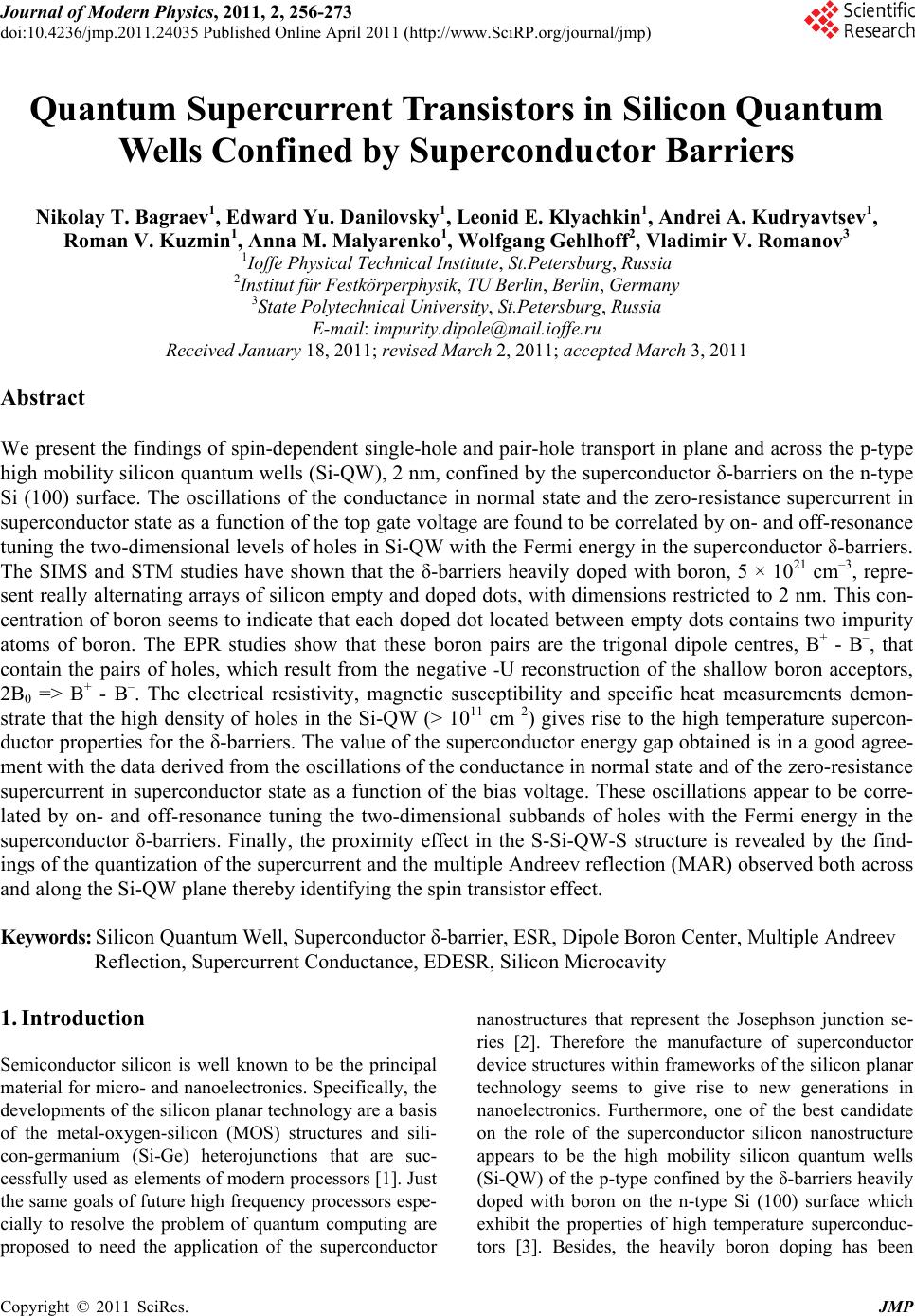
|