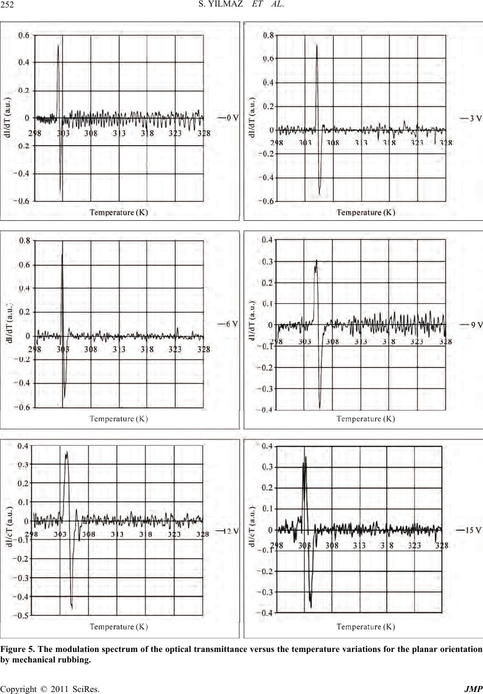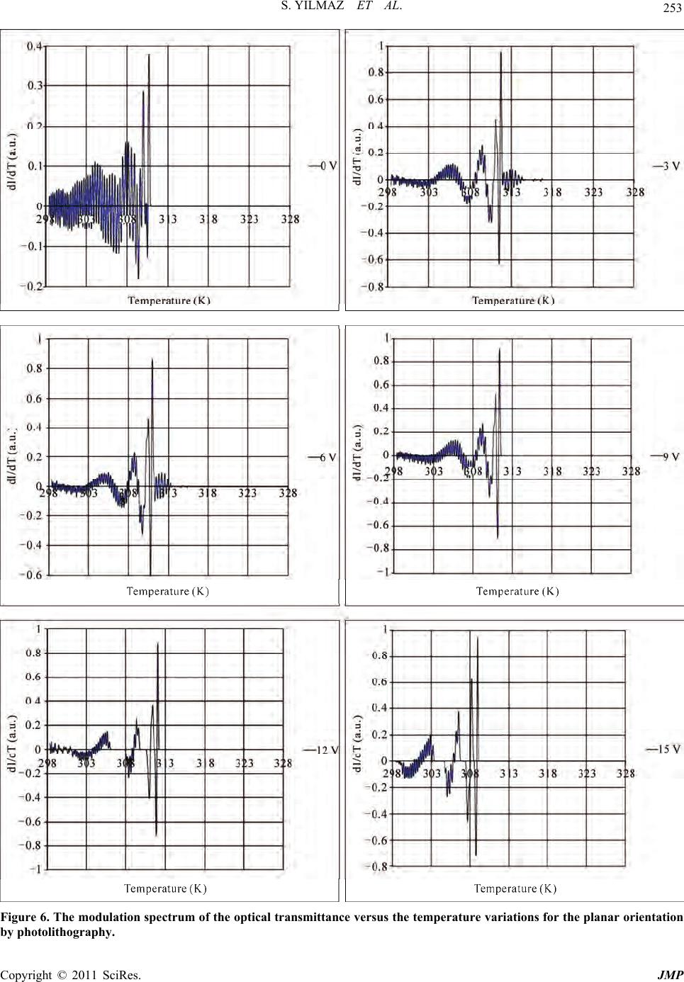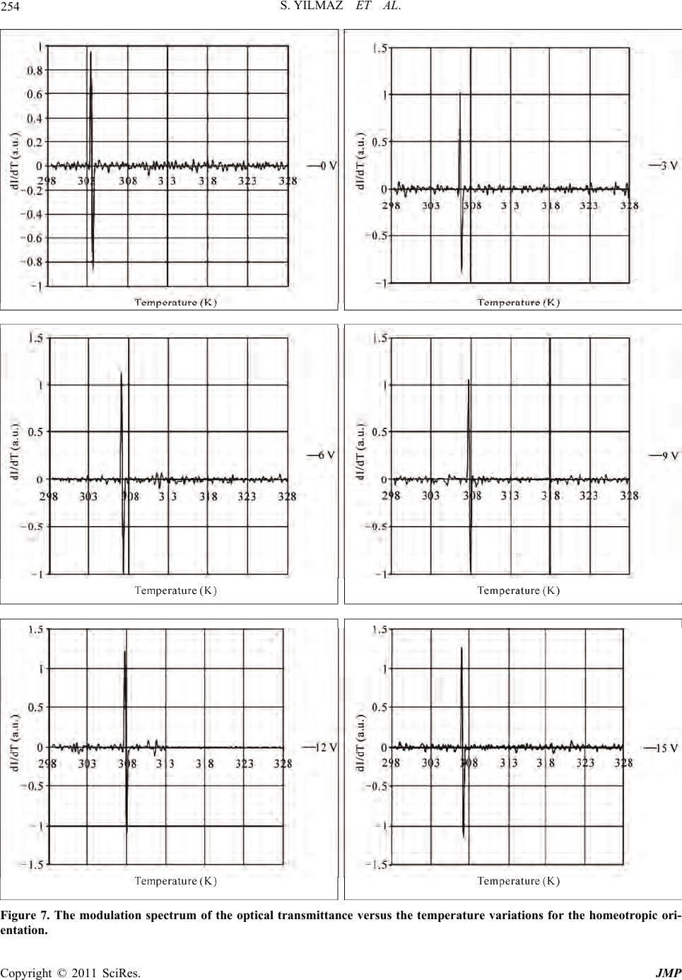
S. YILMAZ ET AL.
Copyright © 2011 SciRes. JMP
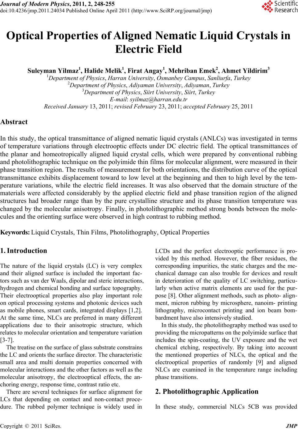
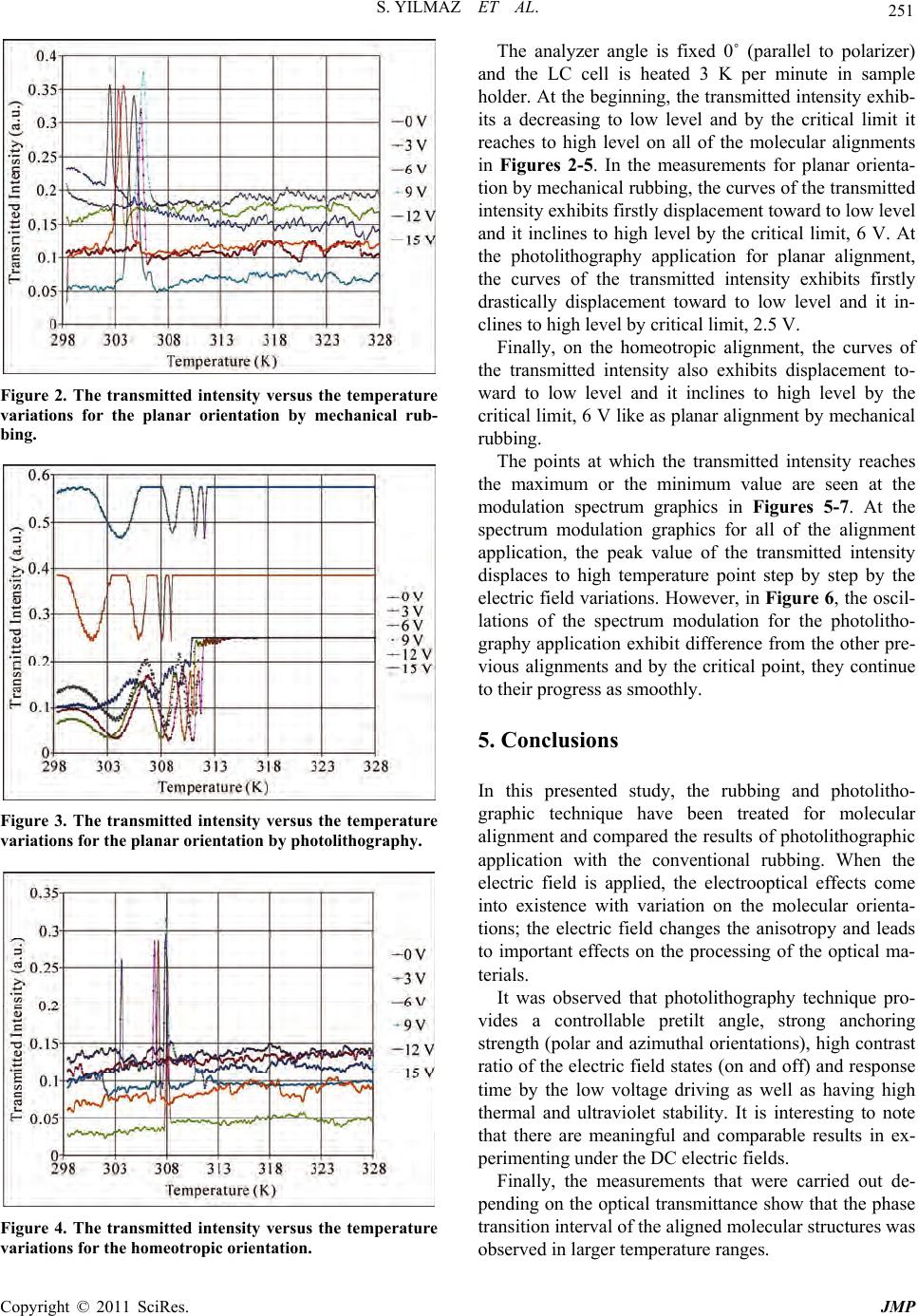
255
The results of this study, which is accomplished on ran-
domly orientated molecules in previous study [16], show
resemblance with the results of other works by devel-
oped in the past studies [17-24].
6. Acknowledgements
The authors thank to Harran University for financial
support. This study is supported by Harran University,
the Fund of Scientific Research Projects (SRP) with
grant no: 919.
7. References
[1] S. Varghese, S. Narayanankutty, C. W. M. Bastiaansen,
G. P. Crawford and D. J. Broer, “Patterned Alignment of
Liquid Crystals by m-Rubbing,” Advanced Materials,
Vol. 16, 2004, pp. 1600-1605.
doi:10.1002/adma.200306536
[2] V. A. Konovalov, V. G. Chigrinov, H. S. Kwok, H. Ta-
kada and H. Takadsu, “Photoaligned Vertical Aligned
Nematic Mode in Liquid Crystals,” Japanise Journal of
Applied Physics, Vol. 43, No. 1, 2004, pp. 261-266.
doi:10.1143/JJAP.43.261
[3] P. G. de Gennes and J. Prost, “The Physics of Liquid
Crystals,” Oxford University Press, UK, 1993.
[4] H. Gleeson, “Introduction to Liquid crystals,” Manches-
ter University Press, UK, 1998.
[5] I. C. Khoo, “Liquid Crystals: Physical Properties and
Nonlinear Optical Phenomena,” John Wiley & Sons, Inc.,
New York, 1995.
[6] P. Klysubun, “Nonlinear Optical Studies of Dye-Doped
Nematic Liquid Crystals,” PhD Dissertation, Virginia
Polytechnic Institute and State University, Virginia, 2002.
[7] S. Yilmaz, and A. Bozkurt, “Spectroscopic Measurement
of Liquid Crystal Anisotropy in the Ultraviolet/Visible
Region,” Materials Chemistry and Physics, Vol. 107, No.
2-3, pp. 410-412.
[8] V. G. Chigrinov, “Liquid Crystal Devices: Physics and
Applications,” Artech House, Boston, 1999.
[9] M. Emek, N. Besli, A. Yildirim and S. Yilmaz, “Optical
Properties of Nematic Liquid Crystal (C21H27NO2S) Un-
der AC/DC Electric Fiel ds” Canadian Journal of Physics,
Vol. 87, No. 4, 2009, pp. 293-298.
doi:10.1139/P09-030
[10] P. Yeh, and C. Gu, “Optics of Liquid Crystal Display,”
John Wiley & Sons, New York, 1999.
[11] S. Kumar, “Liquid Crystals: Experimental Study of
Physical Properties and Phase Transitions,” Cambridge
University Press, Cambridge, 2001.
[12] J. Osterman, L. Madsen, J. Birgerson and K. Skarp, “Op-
tical Properties of Single-Polarizer Reflective Bistable
Nematic Displays,” SID Symposium Digest of Technical
Papers, Vol. 34, 2003, pp. 950-953.
doi:10.1889/1.1832441
[13] D. Kang, J. E. Maclennan, N. A. Clark, A. Zakhidov and
R. H. Baughman, “Electro-Optic Behavior of Liquid-
Crystal-Filled Silica Opal Photonic Crystals: Effect of
Liquid-Crystal Alignment,” Physical Review Letters, Vol.
86, No. 18, 2001, pp. 4052-4055.
doi:10.1103/PhysRevLett.86.4052
[14] S. Yilmaz, “Light Scattering By Some Nematic Liquid
Crystals Due to Phase Transitions,” Journal of Quanta-
tive Spectroscopy and Radiative Transfer, Vol. 104, No.
3, 2007, pp. 305-309. doi:10.1016/j.jqsrt.2006.02.002
[15] J. Osterman, “Investigations of Optical Properties and
Photo-Alignment in Bistable Nematic Liquid Crystal
Displays,” PhD Dissertation, Uppsala University, Sweden,
2005.
[16] S. Yilmaz, “Optical Properties of Some Mixed Nematic
Liquid Crystals in Electric Field,” Materials Chemistry
and Physics, Vol. 110, No. 1, 2008, pp. 140-144.
doi:10.1016/j.matchemphys.2008.01.027
[17] Y. Suzuki, N. Mizoshita, K. Hanabusa and T. Kato,
“Homeotropically Oriented Nematic Physical Gels for
Electrooptical Materials,” Journal of Materials Chemistry,
Vol. 13, No. 12, 2003, pp. 2870-2874.
doi:10.1039/b308098f
[18] R. Bartolino, N. Scaramuzza, D. E. Lucchetta, E. S. Ba-
rna, A.Th. Ionescu and L.M. Blinov, “Polarity Sensitive
Electrooptical Response in a Nematic Liquid Crystal-
Polymer Mixture,” Journal of Applied Physics, Vol. 85,
No. 5, 1999, pp. 2870-2874. doi:10.1039/b308098f
[19] H. Y. Chen and W. Lee, “Electro-Optical Characteristics
of a Twisted Nematic Liquid-Crystal Cell Doped with
Carbon Nanotubes in a DC Electric Field,” Optical Re-
views, Vol. 12, No. 3, 2005, pp. 223-225.
doi:10.1007/s10043-005-0223-7
[20] J. G. Yoo, B. S. Song and J. Kim, “Surface Pretilt Effects
of Bistable Twisted Nematic Liquid Crystal Display,”
Japanise Journal of Applied Physics, Vol. 38, No. 10,
1999, pp. 6005-6007. doi:10.1143/JJAP.38.6005
[21] H. L. Margaryan and V. M. Aroutiounian, “Influence of
Longitudinal Electric Field on Time Characteristics of
Freedericksz Transition,” Moleculer Crystals and Liquid
Crystals, Vol. 454, No. 1, 2006, pp. 513-523.
[22] J. W. Han, “Effect of the Nematic-Isotropic Phase Tran-
sition on the Electro-Optical Characteristics of Polimer-
Dispersed Liquid Crystal Films,” Journal of the Korean
Physical Society, Vol. 40, No. 5, pp. 849-855.
[23] T. Takematsu, H. Okada and H. Onnagawa, “Characteris-
tics of Modulated Microdomain Switching Using Nematic
Liquid Crystals,” Japanese Journal of Applied Physics,
Vol. 41, No. 2A, 2002, pp. 733-736.
doi:10.1143/JJAP.41.733
[24] J. Merlin, E. Chao, M. Winkler and K. D. Singer, P.
Korneychuk and Y. Reznikov, “All-Optical Switching in
a Nematic Liquid Crystal Twist Cell,” Optics Express,
Vol. 13, No. 13, 2005, pp. 5024-5029.
doi:10.1364/OPEX.13.005024