 Journal of Power and Energy Engineering, 2014, 2, 500-508 Published Online April 2014 in SciRes. http://www.scirp.org/journal/jpee http://dx.doi.org/10.4236/jpee.2014.24068 How to cite this paper: França, B.W., da Silva, L.F., Aredes, M., Gerencer, R., Ferreira, D.A. de C. and Siqueira, M.J.V. (2014) Performance Analysis and Technical Feasibility of an iUPQC in Industrial Grids. Journal of Power and Energy Engineering, 2, 500-508. http://dx.doi.org/10.4236/jpee.2014.24068 Performance Analysis and Technical Feasibility of an iUPQC in Industrial Grids Bruno W. França1, Leonardo F. da Silva1, Maurício Aredes1, Roberto Gerencer2, David A. de C. Ferreira2, Maria J. V. Siqueira3 1Department of Electrical Engineering, Federal University of Rio de Janeiro (COPPE/UFRJ), Rio de Janeiro, Brazil 2ADELCO Sistemas de Energia, Barueri, Brazil 3EDP Bandeirante, São Paulo, Brazil Email: aredes@lemt.ufrj.br, d avid .fer reira @ad elco. co m.br , jovita@edpbr.com.br Received December 2013 Abstract The iUPQC is a Unified Power Quality Conditioner in which the series converter emulates a sinu- soidal current source and the shunt converter emulates a sinusoidal voltage source. This approach provides indirect power quality compensation of the load voltage and the source current. Recent studies have suggested that the iUPQC has technical advantages in comparison with the conven- tional UPQC due to its reduced switching frequency characteristic. In this paper, these technical advantages are investigated. Thus, the iUPQC performance is verified through a 150 kVA industri- al equipment and technical design specifications are discussed: the iUPQC power circuit design, the converters arrangement and the driver configuration. Experimental results are provided to validate the technical feasibility and power quality compensation performance. Keywords Unified Power Quality Conditioner; iUPQC; Industrial Power Rate; Active Filter 1. Introduction The Unified Power Quality Conditioner, UPQC, is a worthwhile equipment that provides power quality com- pensation since it is able to mitigate power quality issues of the utility current and of the load voltage, simulta- neously. In this way, many studies have been focused on improving the UPQC effectiveness and robustness, as well as ensuring its viability in high power grids [1-4]. The viability aforementioned is mostly compromised by the converters switching performance because of the harmonic components synthesis for active filter compensations, reaching unviable switching losses in high power converters. Aiming to soften this weakness and provide faster dynamic performance, a dual topology of the conventional UPQC interchanges the source mimicked by the series and shunt converters [5-10], even though still using the same power-circuit configuration (Figure 1). This topology, named iUPQC or dual UPQC, controls the series converter as a sinusoidal current source and the shunt converter as a sinusoidal voltage source. Therefore, the harmonic components are mitigated without being handled by the iUPQC controller, improving its dynamic performance. 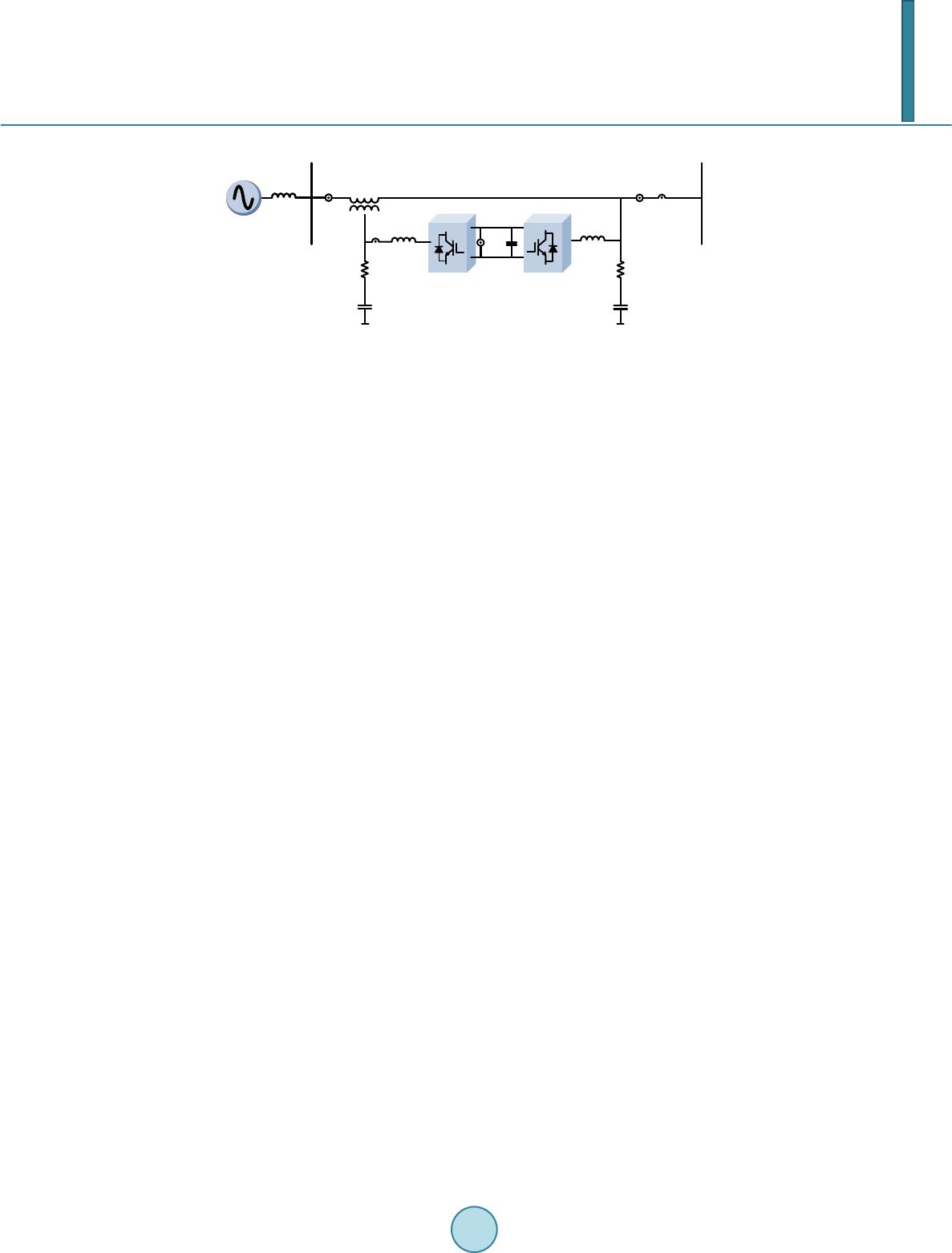 B. W. França et al. Figure 1. iUPQC Power circuit configuration. In [8] the iUPQC performance was investigated using different switching frequencies. Experimental results from a laboratorial prototype have indicated that the iUPQC harmonic compensation is achieved even if a re- duced switching frequency is employed. This suggested that the iUPQC is more appropriated than the conven- tional UPQC for power quality compensation in high power system, when a reduced switching frequency should be employed to obtain reduced switching losses and, consequently, reach its viability with the power converters currently available. This paper carries out the iUPQC power quality compensation in an industrial power rate system. Thus, tech- nical aspects are discussed according to the procedures performed to attain a 150 kVA iUPQC connection into the grid. In Section 2, the iUPQC power circuit design is discussed through the power flow analysis for proper dimensioning of the power components. The iUPQC commissioning tests are presented in Section 3 with the proper procedures to assure the power converters switching feasibility at nominal conditions. In Section 4, the provided experimental results present the transitory and steady-state iUPQC performances for the stated adjust- ments and nominal conditions. 2. iUPQC Power Circuit Design The iUPQC power components are designed to allow the iUPQC operation with nominal load. Moreover, the steady-state active and reactive power flows in the aforementioned situation are used for dimensioning the pow- er components appropriately. The iUPQC used in this work is aimed to perform sag/swell voltage compensation up to 50% of the nominal voltage with full load (150 kVA). Figure 2 depicts this situation. Moreover, this power quality issue associated with the nominal load connection provides the maximum steady-state overload situation of the iUPQC compo- nents. Therefore, this scenario provides a satisfactory condition for the iUPQC components design. In a sag/swell source voltage disturbance, the iUPQC preserves the load bus voltage regulation and thus a voltage compensation (VC) rises at the series coupling transformer. This voltage is a positive-sequence compo- nent at the fundamental frequency. According to the circuit, the voltage phasors of the positive-sequence com- ponent at fundamental frequency can be expressed as: (1) Therefore, disregarding the system losses, the power flow in steady-state is: (2) (3) (4) (5) where Equations (2)-(4) guarantee unit power factor at the source bus, and Equation (5) the power flow balance. The load current highlighted in Figure 2 is due to the active power load consumption. In a sag/swell voltage disturbance, the voltage and this load current cause an active power flow from the series converter to the system. Since Equation (5) must be satisfied in steady-state, this active power flows through the shunt converter, resulting in an internal circulating current (sag/swell current). Both currents (load and sag/swell currents) with Source bus i f V s V L i L V DC Load bus Series converter Shunt converter 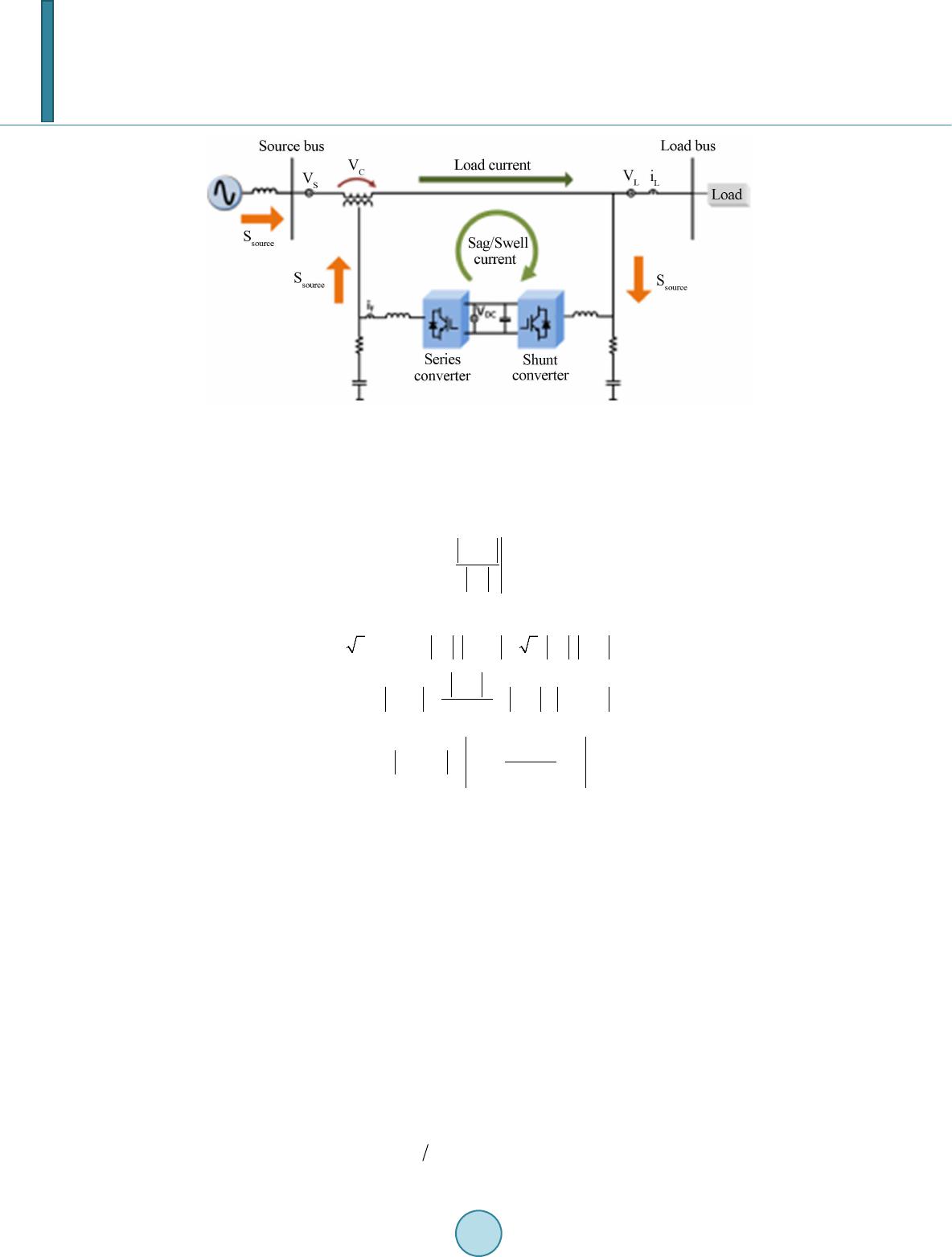 B. W. França et al. Figure 2. iUPQC with full load and 50% sag/swell compensation. the highest amplitude in steady-state should be taken into account to the iUPQC components design. For the branch between the source and the load buses, the highest current is achieved when only average ac- tive power is being consumed by the load further with the maximum sag/swell voltage disturbance. Thus, defin- ing a constant ( ) for the maximum allowable sag/swell voltage disturbance: / max / source sag swell Nsag swell V kV = (6) From (2): / 33 sag swellNsourceNload k VIVI⋅⋅⋅ =⋅⋅ / / load sourceloadsag swell sag swell I I II k == + (7) // 11 sag swellloadsag swell II k = − (8) Therefore, Equation (8) indicates that the iUPQC components has to be designed to support currents in steady-state with amplitude values higher than the nominal load current amplitude, due to the voltage regulation of the load bus. It is important to highlight that high values will be achieved to sag voltage disturbances. Never- theless, if the series converter is able to operate at higher voltage amplitudes, the coupling transformer can be useful to reduce the current in the series converter branch. 3. iUPQC Commissioning Tests The industrial iUPQC parameters are shown in Table 1. These values were specified according to usual values of voltage, frequency and power rate in Brazilian industrial power grids. However, before connecting the iUPQC into the grid, commissioning tests were performed to certify the safe operation of the equipment in no- minal conditions. The commissioning tests are important to ensure safe conditions to the power converters switching. As a re- sult, the switching devices parameters and frequency are established. The switching devices are composed by 6 drivers Semikron SKHI23 and 12 IGBT’s SKM 400 GB 176 D with snubber . Even though the switching devices are set according to the power rate, nominal voltage and switching fre- quency values, the power converter design as well the constructive arrangement of the equipment can cause un- safe operational conditions due to electromagnetic interference (EMI). The EMI are originated from the IGBT switching and are also produced by high output voltages and/or inductive load current switching [1 1-13].  B. W. França et al. Table 1. iUPQC parameters. Parameter Value Voltage 440 V rms Grid frequency 60 Hz Power rate 150 kVA DC-link voltage 850 V dc DC-link capacitors C = 36267 µF Shunt converter passive filter L = 170.0 µH R = 1.0 Ω C = 300.0 µF Series converter passive filter L = 340.0 µH R = 2.0 Ω C = 150.0 µF Sampling frequency 5130.0 Hz Moreover, the EMI may adversely affect the driver operation. In order to mitigate the EMI, Figure 3 depicts the converters arrangement, where the drivers are placed just in the back-side of the IGBT connection buses. This should reduce the EMI in the drivers due to the electromagnetic isolation provided by the metallic sheet between the drivers and the IGBT busses, and also due to the resultant short cables that connect the drivers to the IGBTs. In the commissioning tests, the first approach set the driver components at the following values: , , and dead time . According to the driver data- sheet, these values may be adjusted to avoid additional losses or even the destruction of the IGBT. Hence, the commissioning test was accomplished as shown in Figure 4, in order to obtain reduced collector emitter voltage ( ) spike with appropriated switching frequency and dead time. The commissioning test procedure is performed by increasing the ac voltage ( ) and current ( ) through the PWM control and the variable load, respectively. The dc voltage ( ) was regulated to 700V. Then, the voltage was verified in order to obtain acceptable spike values, according to the IGBT datasheet. For the first approach values, Figure 5 depicts the voltage when and . The spike voltage reached unacceptable values (about ). The second approach increased the resistances values to . This is the recommended driver datasheet procedure to fit to the equipment application. As depicted in Figure 6, acceptable spike values were achieved with and . The results obtained through and adjustments guarantee the iUPQC safe operation with a switching frequency of 5130.0 Hz and dead-time of 5 μs. As the iUPQC converters synthesize sinusoidal refer- ences, these frequency and dead-time values should be enough to allow the active filter capability. 4. Experimental Results and Design Changes After successful accomplish commissioning tests in the series and shunt converters, the iUPQC is ready to be connected to the system. Nevertheless, a design change in the shunt converter passive filter configuration can bring additional benefits in the equipment performance. In this way, the arrangement of the passive filter of the shunt converter was modified with the RC branch connected at the load bus, instead of the conventional connection displayed in Figure 1, where it is connected together with the passive filter inductor. This change allows the RC branch current measurement by the iL cur- rent sensor. In other words, the RC branch current is measured as the branch was a load and thus this current will be also compensated by the iUPQC. The harmonic current compensation was verified through the iUPQC performance with a three-phase full bridge diode rectifier. Figure 7 shows the steady-state harmonic compensation and Figure 8 shows the transi- tory response through the load connection. Despite the reduced switching frequency due operational requirement 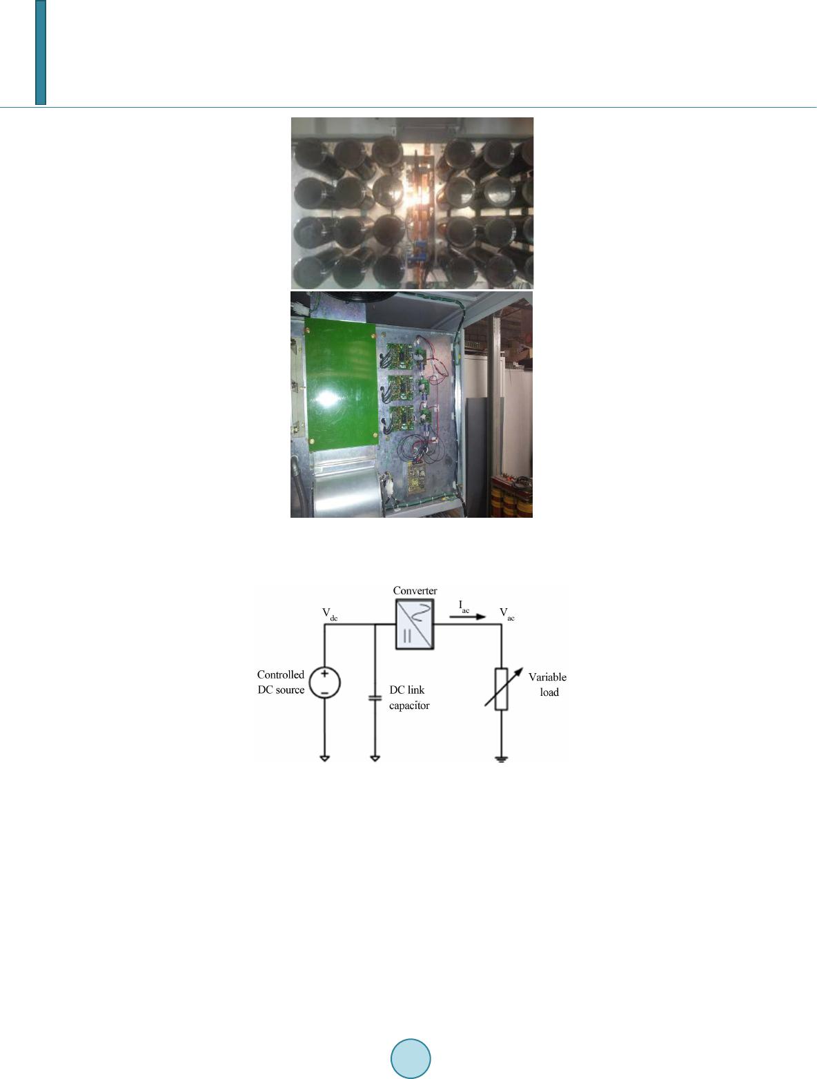 B. W. França et al. Figure 3. Converters arrangement; (a) detail of the IGBT buses and (b) Driver placed in the converter back-side. Figure 4. Commissioning test. (5130.0 Hz) the harmonic current THD was reduced from approximately 25% at the load bus to 7.5% at the source bus. Moreover, the iUPQC achieve fast dynamic response, reaching the steady-state with sinusoidal waveform in approximately 4 cycle’s period. These favorable results can be attributed to the iUPQC control strategy, which does not synthesize the harmonic components to compensate them. For a two-phase load connection, the iUPQC controller has to synthesize sinusoidal three-phase currents at the series converter. In this manner, this three-phase current will supply the average active power of the load and the unbalanced current will be supplied by the shunt converter. Figur es 9 and 10 depict the experimental results of a two-phase full bridge diode rectifier connected at the load bus with the three-phase current drawn at the source bus. It is important to highlight that the source currents are three-phase sinusoidal currents with reduced harmonic and unbalanced components, in spite of the unbalanced two-phase harmonic load currents drawn at the load bus (two-phase diode rectifier). Figure 11 depicts the voltage regulation in steady-state with the two-phase load aforementioned. The rms- 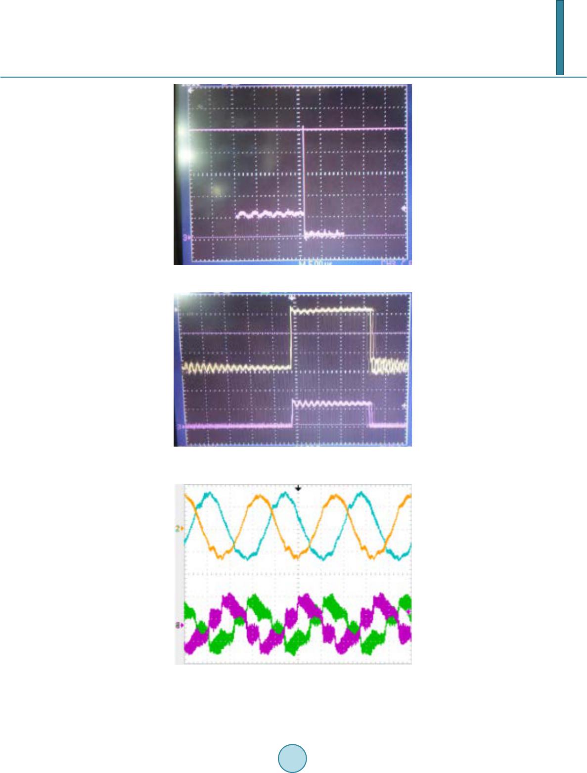 B. W. França et al. Figure 5 . IGBT collector emitter voltage. 5 μs/div, 500 V/div. Figure 6. IGBTs collector emitter voltage. 5 μs/div, top signal 500 V/div and bottom signal 500 V/div. Figure 7. Source current compensation in steady-state with three- phase full bridge diode rectifier; load currents (pink and green) and com-pensated source currents (yellow and blue); 5 ms/div, 100 A/div.  B. W. França et al. Figure 8. Source current compensation in transitory load con- nection with three-phase full bridge diode rectifier; load currents (pink and green) and compensated source currents (yellow and blue); 5 ms/div, 100 A/div. Figure 9. Source current compensation in steady-state with two-phase full bridge diode rectifier; load current (pink) and three-phase compensated source currents (yel- low, blue and green); 5 ms/div, 100 A/div. Figure 10. Source current compensation in transitory load connection with two-phase full bridge diode rectifier; load current (pink) and three-phase compensated source currents (yellow, blue and green); 5 ms/div, 100 A/div. 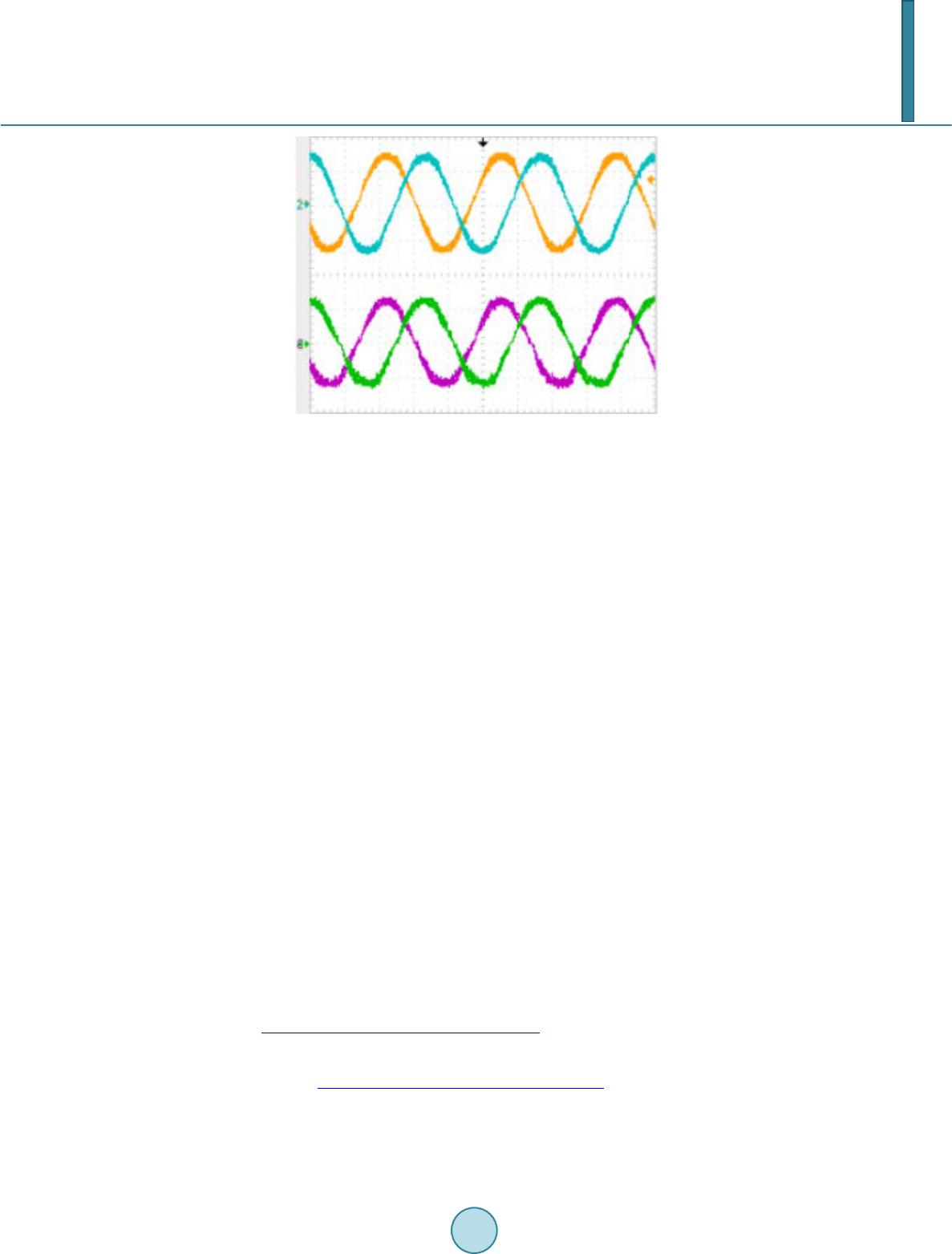 B. W. França et al. Figure 11. Load voltage regulation in steady-state with two- phase full bridge diode rectifier; source voltage (yellow and blue) and compensated load voltages (pink and green); 5 ms/div, 500 V /d iv . load voltage was regulated around the nominal value even with a swell voltage disturbance at the source bus. Moreover, the voltage unbalance at the load bus was retained in acceptable values in face of the unbalanced load. 5. Conclusions The iUPQC design specifications were discussed to an industrial power rate equipment. In this way, the compo- nents design can be obtained through the equipment power rate, the maximum sag/swell voltage regulation ca- pability and the nominal power load consumption. Commissioning tests were used in order to verify the iUPQC operation viability due to the collector emitter voltage spikes which could damage the converters switching devices. In addition to the proper configuration of the driver components, the commissioning tests are also useful to determine the allowable maximum switching frequency and minimum dead-time of the IGBTs. The iUPQC performance was verified after the commissioning tests adjustments. Thus, despite the reduced switching frequency adopted, the iUPQC performance guarantees the harmonic source current mitigation and the load voltage regulation with balanced and unbalanced harmonic loads. Acknowledgements The authors thanks to Brazilian Electricity Regulatory Agency (ANEEL) which yielded the feasibility of this study through the P&D “Desenvolvimento de um Compensador Universal com correção de VTCD-iUPQC”. References [1] Haid ar, A.M. A. , Benach aiba, C., Ibrahim, F. and Hawari, K. (2 011) Parameters Evaluation of Unified Power Quality Conditioner. 2011 IEEE International Conference on Electro/Information Technology (EIT). [2] Kh ad kikar, V. and Chandra, A. (2008) A New Control Philosophy for a Unified Power Quality Conditioner (UPQC) to Coordinate Load-Reactive Power Demand between Shunt and Series Inverters. IEEE Transactions on Power Delivery, 23, 2522-2534. http://dx.doi.org/10.1109/TPWRD.2008.921146 [3] Melin, P., Espinoza, J., Moran, L., Rodriguez, J., Cardenas, V., Baier, C. and Munoz, J. (20 12) Analysis, Design and Control of a Unified P owe r -Quality Conditioner Based on a Current-Source Topology. IEEE Transactions on Power Delivery, 27, 17 27-17 36 . http://dx.doi.org/10.1109/TPWRD.2012.2199524 [4] Mokhtatpour, A. and Shayan far, H. (20 11) Power Quality Compensation as Well as Power Flow Control Using of Uni- fied Power Quality Conditioner. Power and Energy Engineering Conference (APPEEC). [5] Aredes, M. and Fern and es, R. (2009) A Dual Topology of Unified Power Quality Conditioner: The iUPQC. 13th Eu-  B. W. França et al. ropean Conference on Power Electronics and Applications. [6] Aredes, M. and Fernandes , R. (200 9 ) A Unified Power Quality Conditioner with Voltage SAG/SWELL Compensation Capability. COBEP’09 Brazilian Power Electronics Conference. [7] B. Franca and M. Aredes, (2011) Comparisons between the UPQC and its dual topology (iUPQC) in dynamic response and steady-state. em IECON 2011 - 37th Annual Conference on IEEE Industrial Electronics Society,. [8] Fran ca, B., Rolim, L. and Aredes , M. (2011) Frequency Switching Analysis of an iUPQC with Hardware-in-the-Loop Development Tool. Proceedings of the 2011-14th European Conference on Power Electronics and Applications (EPE 2011). [9] Fran ca, B., da Silva, L. an d Aredes, M. (2011) Comparison between Alpha-Beta and DQ-PI Controller Applied to IUPQC Oper atio n. Power Electronics Conference (COBEP). [10] dos Santos, R.M., Mezarob, M. and da Cunha, J. (2011 ) A Dual Unified Power Quality Conditioner Using a Simplified Control Technique. Power Electronics Conference (COBEP). [11] Akagi, H. an d Shimizu, T. (2008 ) Attenuation of Conducted EMI Emissions from an Inverter-Driven Motor. IEEE Transactions on Power Electronics, 23, 282-290 . [12] P ei, X., Zhang, K., Kang, Y. and Ch en, J. (2004) Analytical Estimation of Common Mode Conducted EMI in PWM Inverter. 39th IAS Annual Meeting. Conference Record of the 2004 IEEE Industry Applications Conference. [13] Son, Y.-C. and Sul, S. -K. (20 01) Conducted EMI in PWM inverter for household electric appliance. 36th IAS Annual Meeting , Conference Record of the 2001 IEE E Industry Applications Conference.
|