Paper Menu >>
Journal Menu >>
 Circuits and Systems, 2011, 2, 91-100 doi:10.4236/cs.2011.22014 Published Online April 2011 (http://www.SciRP.org/journal/cs) Copyright © 2011 SciRes. CS A Scalable Model of the Substrate Network in Deep N-Well RF MOSFETs with Multiple Fingers Jun Liu1,2, Maris sa Condon2 1Key Laboratory of RF Circuits and Systems, Ministry of Education, Hangzhou Dianzi University, Hangzhou, China 2School of Electronic Engineering, Dublin City University, Dublin, Ireland E-mail: ljun77@163.com Received January 18, 2011; revised March 4, 2011; accepte d M arch 11, 2011 Abstract A novel scalable model of substrate components for deep n-well (DNW) RF MOSFETs with different num- ber of fingers is presented for the first time. The test structure developed in [1] is employed to directly access the characteristics of the substrate to extract the different substrate components. A methodology is developed to directly extract the parameters for the substrate network from the measured data. By using the measured two-port data of a set of nMOSFETs with different number of fingers, with the DNW in grounded and float configuration, respectively, the parameters of the scalable substrate model are obtained. The method and the substrate model are further verified and validated by matching the measured and simulated output admit- tances. Excellent agreement up to 40 GHz for configurations in common-source has been achieved. Keywords: Deep N-Well (DNW), RF Mosfets, Substrate Network, Scalable Model 1. Introduction THE incorporation of a Deep N-Well (DNW) implantation into a standard CMOS technology has become a popular choice for reducing undesired interference in CMOS mixed-signal/RF SoC designs [2-6]. Substrate network parameters are of the utmost importance in accurately modeling the output admittance of RF MOSFETs. For mixed-signal/RF SoC design, a scalable model of RF MOSFETs is useful. Many papers have reported about scalable models of substrate network components [7-13]. However, there are few detailed works on scalable mod- els with substrate network components in DNW RF MOSFETs with different number of fingers. In contrast to the RF MOSFET without DNW implantation (as seen from the nMOSFETs in Figure 1), the DNW actually partitions the substrate of a DNW RF MOSFET into three parts [1]: The DNW itself, the p-well in the DNW, and the original substrate where the DNW is formed. The DNW layer forms a capacitive coupling path in the sub- strate, which exists no matter what the electrical con- figuration is. Furthermore, most previous works [7-19] dealt with substrate parasitic effects in RF MOSFETs by using resistance networks only. The capacitive coupling effect, which is physically in existence, is always ne- glected. All of these make the previously reported sub- strate models less physically reasonable to use for accu- rately extracting the substrate network components of DNW RF MOSFETs. In this paper, a compact, physically based substrate network is proposed targeted specifically at DNW RF MOSFET modeling. A novel test structure proposed in [1] is expanded and employed in deriving and extracting the Nf - dependent equations involving substrate compo- nents in multi-finger DNW RF MOSFETs. The geomet- ric effects such as shallow trench isolation (STI), which have never been considered in previous reported works, are accurately modeled. The results show that the sub- strate components within the p-well and th e capacitances caused by the DNW are strongly dependent on Nf, while the parasitic components in the original p-substrate have a slight depe n dence on Nf in multi-finge r devices. To verify the validity of the derived scalab le model of the substrate network components, a macro-model con- sisting of the BSIM3v3.2 model core with the proposed substrate-network based on the extracted parameters, is simulated in Agilent Advanced Design System (ADS). Excellent agreement between the simulated and meas- ured output admittance for a set of devices with different number of fingers up to 40 GHz validated the accuracy of the methodology proposed for DNW RF-MOSFET modeling in this paper. 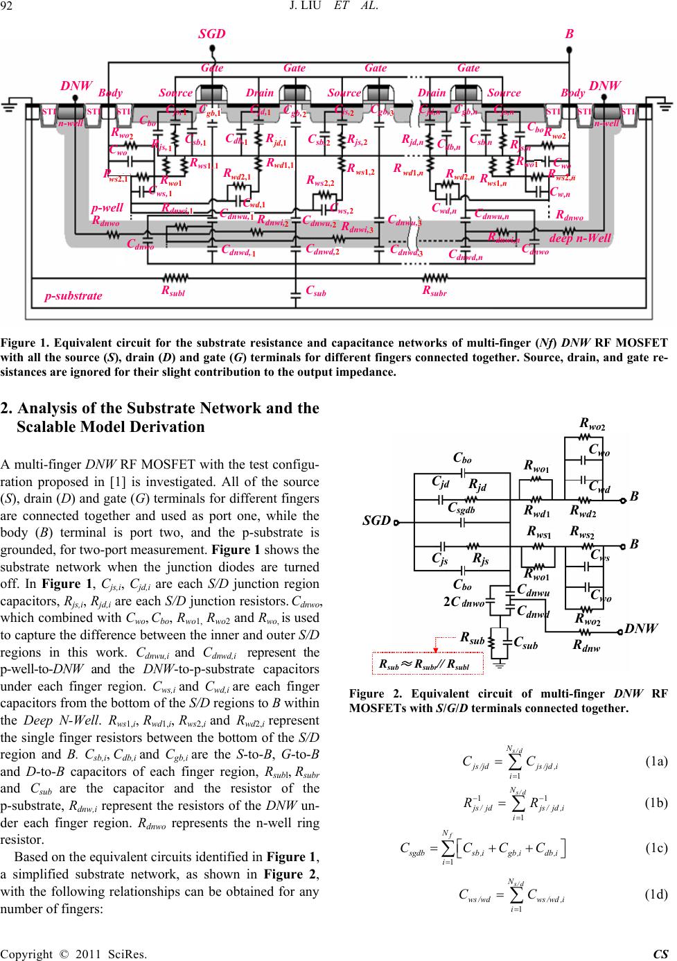 J. LIU ET AL. Copyright © 2011 SciRes. CS 92 DNW C db,1 C gb,1 C bo C js,1 R js,1 C dnwo C sub R subl R subr C ws,1 R ws1,n R ws2,n R ws1,1 C wo R wo2 C wo R wo2 C dnwo C dnwd,1 C dnwu,1 C dnwd,2 C dnwu,2 C dnwd,3 C dnwu,3 C dnwd,n C dnwu,n C bo C js,n R js,n C sb,1 C jd,1 R jd,1 C gb,n C sb,2 C gb,2 C js,2 R js,2 C gb,3 C db,n C sb,n C jd,n R jd,n R ws2,1 R wd2,1 R wd1,1 C wd,1 R ws2,2 R ws1,2 C ws,2 R wd2,n R wd1,n C wd,n C w,n p-substrate p-well STI STISTI STI SourceDrainSourceDrain Source GateGate GateGate deep n-Well Body Body R dnwo R dnwo R dnwi,n R dnwi,3 R dnwi,2 R dnwi,1 B S GD n-well n-well STISTI DNW R wo1 R wo1 Figure 1. Equivalent circuit for the substrate resistance and capacitance networks of multi-finger (Nf) DNW RF MOSFET with all the source (S), drain (D) and gate (G) terminals for different fingers connected together. Source, drain, and gate re- sistances are ignored for their slight contribution to the output impedance. 2. Analysis of the Substrate Network and the Scalable Model Derivation A multi-finger DNW RF MOSFET wi th the test configu- ration proposed in [1] is investigated. All of the source (S), drain (D) and gate (G) terminals for diff erent fingers are connected together and used as port one, while the body (B) terminal is port two, and the p-substrate is grounded, for two-port measurement. Figure 1 shows the substrate network when the junction diodes are turned off. In Figure 1, Cjs,i, Cjd,i are each S/D junction region capacitors, Rjs,i, Rjd,i are each S/D junction resistors. Cdnwo, which combined with Cwo, Cbo, Rwo1, Rwo2 and Rwo, is used to capture the difference between the inner and outer S/D regions in this work. Cdnwu,i and Cdnwd,i represent the p-well-to-DNW and the DNW-to-p-substrate capacitors under each finger region. Cws,i and C wd,i are each finger capacitors from the bottom of the S/D regions to B within the Deep N-Well. Rws1,i, Rwd1,i, Rws2,i and R wd2,i represent the single finger resistors between the bottom of the S/D region and B. Csb,i, Cdb,i and Cgb,i are the S-to-B, G-to-B and D-to-B capacitors of each finger region, R subl, Rsubr and C sub are the capacitor and the resistor of the p-substrate, Rdnw,i represent the resistors of the DNW un- der each finger region. Rdnwo represents the n-well ring resistor. Based on the equivalen t circuits iden tified in Figure 1, a simplified substrate network, as shown in Figure 2, with the following relationships can be obtained for any number of fi ng ers : B C bo C sgdb C jd R js 2C dnwo R sub C js R ws1 R jd R wd1 C sub B C dnwd C dnwu C bo C wd R wd2 SGD R ws2 C ws C wo R wo2 R wo2 C wo R dnw DNW R sub ≈ R subr // R subl R wo1 R wo1 Figure 2. Equivalent circuit of multi-finger DNW RF MOSFETs with S/G/D terminals connected together. 1 s/d N j s /jdjs /jd ,i i CC (1a) 11 1 s/d N j s /jdjs/jd ,i i RR (1b) 1 f N s gdbsb,igb,idb,i i CCCC (1c) 1 s/d N ws /wdws /wd ,i i CC (1d) wo1 wd2,1 wd,1 wd1,1 jd,1 ws1,2 wd1,n 3 2 2 2,2 2 2 1 1 2 1 12 3 2 2 1 wo2 1 ws1,n wd 2 , n 1 1 1 1 2 3 3 1 1 ws2 , 1 2 1 2 2 1 1 1 2 2C g b,1 ws2 , n  J. LIU ET AL. Copyright © 2011 SciRes. CS 93 11 11 11 1 s/d N ws/ wdws/ wd,i i RR (1e) 111 s ubsubl subr RRR (1f) 11 22 22 1 s/d N ws/ wdws/ wd,i i RR (1g) 1 f N dnwu dnwu,i i CC (1h) 1 f N dnwddnwd ,i i CC (1i) 1 1 1 2f N dnw dnwodnw,i i RR R (1j) where, Cjs, Cjd represent the total S/D junction region capacitances, Rjs,, Rjd represent the total S/D junction re- sistances, Rsub represents the total resistance of the p-substrate, Cdnw represents the total capacitance caused by the DNW, Cws, Cwd are the total capacitances from the bottom of the S/D regions to B within the Deep N-Well, Rws1/wd1 and Rws2/wd2 are the total resistances between the bottom of the S/D regions and B within the Deep N-Well and Ns and Nd represent the numbers of source and drain diffusion regions, respectively. In the model, when the number fing ers is odd, Ns = Nd = (Nf + 1)/2. Ns = Nf/2 + 1 and Nd = Nf/2 when the number of fingers is even. Assuming that there are no differences in the inner S/D regions, the above equations, (1a)-(1h), can be formed as follows: j s/jds/dj,i CNC (2a) j s/ jdj/is/d RRN (2b) 2 s gdbfsdb,igb,i CNCC (2c) ws/wds/ dw,i CNC (2d) 1 11 w,i ws/wd s /d R RN (2e) 2 22 w,i ws/wd s /d R RN (2f) dnwuf dnwu,i CNC (2g) dnwdfdnwd,i CNC (2h) 2dnwi dnw dnwo f R RRN (2i) where j ,i js,i jd,i CC C j ,i js,i jd,i RR R, s db sb,idb,i CCC w,iws,iwd,i CC C ,11 1w,iws,iwd,i RR R and 22 2w,iws,iwd,i RR R. In this paper, the following equations are used to em- pirically model the Nf - dependence of Rsub and Csub: s ubsubIfsubunit RRNR (2j) s ubsubIfsubunit CC NC (2k) where RsubI and CsubI represent the p-substrate resistance and capacitance of a one-finger device, Rsubunit and Csubunit are used to explain the increase in Rsub and Csub with the increase in the number of gate fingers. 3. Scalable Model Parameter Extraction In order to accurately predict the scalability of the sub- strate elements, a direct parameter extraction methodol- ogy is of the utmost importance. In this work, two dif- ferent test configurations are used. One has the DNW floating (as shown in Figure 3(a)) and the other has the DNW grounded (as shown in Figure 4(a)). In each case, all S/D/G terminals for different fingers are connected together as port one, the B terminal is port two, and the p-substrate grounded. The equivalent circuits shown in Figure 3(b) and Figure 4(b) can easily be derived from the complete equivalent circuit shown in Figure 2, for SSSSSSS DDDDDDD SS Source (S) Drain (D) Gate (G) SGD DNW Metal Level 1( M1 )n-well Body (B) (a) (M1) D N W n-well  J. LIU ET AL. Copyright © 2011 SciRes. CS 94 B C bo C sgdb C jd R js 2C dnwo R sub C js R ws1 R jd R wd1 C sub B C dnwd C dnwu C bo C wd R wd2 B SGD C j R j C w R w1 R w2 C dnw C sub R sub C w ≈ C ws //C wd //2C wo ,C j ≈ C js // C jd R j ≈ R js // R jd , R w1 ≈ R wd1 // R ws1 //(R wo1 /2) R w2 ≈ R wd2 //R ws2 // (R wo2 /2) C sgdbt ≈ C sgdb //2C bo, R ws2 C ws C wo R wo R wo C wo C sgdbt C dnw ≈ 2C dnwo //[C dnwu C dnwd /(C dnwu +C dnwd )] SGD Z L Z MF Z R R wo1 R wo1 (b) (c) Figure 3. (a) Simplified layout plane figure of DNW RF-MOSFETs with S/G/D terminals connected together , while the DNW is floating. (b) Equivalent circuit model for the device shown in Figure 3(a). Rdnw is ignored for its slight influence on two-port measurement. (c) Simplified equivalent circuit for parameter extraction. SSSSSSS DDDDDDD SS Source (S) Drain (D) Gate (G) SGD Metal Level 1( M1 )n-well Body (B) DNW (a) B C bo C sgdb C jd R js 2C dnwo C js R ws1 R jd R wd1 B C dnwu C bo C wd R wd2 B SGD C j R j C w R w1 R w2 C dnwuo C w ≈ C ws //C wd //2C wo ,C j ≈ C js // C jd R j ≈ R js // R jd ,R w2 ≈ R wd2 //R ws2 // (R wo2 /2) C sgdbt ≈ C sgdb //2C bo, R ws2 C ws C wo R wo2 R wo2 C wo C sgdbt C dnwuo ≈ 2C dnwo //C dnwu SGD R dnw R dnw Z L Z MG Z R R wo1 R wo1 R w1 ≈ R wd1 //R ws1 // (R wo1 /2) (b) (c) Figure 4. (a) Simplified layout plane figure of DNW RF-MOSFETs with S/G/D terminals connected together, with the DNW grounded. (b) Equivalent circuit mode l for devic e show n in Figure 4(a). Since Rdnw is much smaller than Rsub, the contribution of Cdnwd, Rsub and Csub to Z-parameters becomes so slight that it can be ignored. (c) Simplified equivalent circuit for parameter extraction. modeling the above two test structures (e.g., with the DNW in grounded or float configuration, respectively). 1 wd1 wd2 ws2 ws1 wo1 2 w2 w1 1111 222 2 2 2, 2 2, ,2 dnwdnwodnwu dnwddnwudnwd sgdbtsgdbbo wwdwswo wws wdwojjsjd jjsjd wwdwswo CC CCCC CC CRRRR CCCCCCC RR RRRRR (M1) n-well DNW wo2 wo1 wd2wd1 ws2 ws1 wo1 wo2 w2 2 111 1 222 2 2 2, 2, 2 ,2 dnwuodnwo dnwu wws wdwoj jsjd sgdbtsgdbbo wwdwswo jjsjd wwdwswo CCC CCCCCCC CC CRRRR RR RRRRR w1  J. LIU ET AL. Copyright © 2011 SciRes. CS 95 As seen from Figure 3(b) and Figure 4(b), since the topologies from S to B are the same as that from D to B, both of the equivalent circuits shown in Figure 3(b) and Figure 4(b) can be reduced to T-networks by using sim- ple approaches as shown at the bottom of Figure 3(c) and Figure 4(c). Based on (2a)-(2i) and the approaches used to simplify Figure 3(b) and Figure 4(b) to Figure 3(c) and Figure 4(c), respectively, the elements of the two T-networks shown in Figure 3(c) and Figure 4(c) can be calculated with the following equations: 1 j fj,i CN C (3a) 1 jj,if RR N (3b) 21 wwofw,i CCNC (3c) 11 1 11 05 1 05 1 wow ,if w wow,if .R RN R.R RN (3d) 22 2 22 05 1 05 1 wow ,if w wow ,if .R RN R.R RN (3e) 22 s gdbtbofsdb,i gb,i CCNCC (3f) 2 dnwuodnwofdnwu,i CCNC (3g) 2 dnwdnwofdnw,i CCNC (3h) where dnwu,idnwd ,i dnw,i dnwu,idnwd ,i CC CCC (3h.1) Using (3h.1), Cdnw,i can be calculated as follows: dnwu,i dnw,i dnwd ,i dnwu,idnw,i CC CCC (3h.2) (2c), (2g)-(2k) and (3a)-(3h) give the Nf -dependent eq- uations of the equivalent circuit in Figure 2. This enables the direct identification of the scalability of the substrate components. This will be shown later in this section. As the ZL and ZR of the T-network shown in Figure 4(c) are the same as the ZL and ZR shown in Figure 3(c), with the ground terminal as reference, the Z-parameters of the T-networks shown in Figure 3(c) and Figure 4(c) can be calculated approximately with the following equ- ations: 1 1 11 12 Ldnw_ floating,dnw_ floating, ZZZ 1 11 12 dnw_ grounded ,dnw _ grounded , ZZ 22 222 222 11 jj j s gdbt jj jj CR C jjC CR CR (4a) 22 12 R dnw_floating,dnw_floating, ZZ Z 22 12dnw_ grounded ,dnw_grounded , ZZ 2 22 122 222 2 22 11 www w ww ww RRC Rj RC RC (4b) 12 22 2 1sub MFdnw_ floating, s ub sub R ZZ RC 2 22 2 1 1sub sub dnw sub sub RC jj C RC (4c) 12 1 MGdnw_grounded ,dnwdnwuo ZZ RjC (4d) where Zdnw_floating and Z dnw_grounded are measured Z-para- meters of DNW RF MOSFETs with S/G/D terminals connected together, when the DNW is floating or grounded, respectively. Further, the real and imaginary parts of the above Z-parameter expressions can be rearranged as follows: 22 2 1 1 Re j j j L RCR Z (5a) 1 1 222 Im 1 j sgdbt L j j C CZ CR (5b) 2 22 1 Im w Rww C ZRC (5c) 2 122 2 2 Re 1w wR ww R RZ RC (5d) 112 2 Re M Fsubsub sub Z RRC (5e) 1 2222 Im 1 dnwMFsub subsub sub CZRC/RC (5f) Re dnw MG RZ (5g) 1 Im M G dnwuo ZC (5h) Using (5a) and (5c), Rj and Cw can be extracted from the slopes of the linear regression curves of the experi- menta l 1 2Re L Z and Im R Z versus2 , respectively. (5a) and (5c), after subtracting Rj and Cw, give Cj and Rw2. Further, (5b) and (5d) give Csgdbt and Rw1. Using (5e), Rsub and Csub can be determined from the intercept of the linear regre ssion curve of th e experimen- tal 1 M F Re Zversus 2 , and the slope gives Csub after subtracting Rsub. After subtracting Rsub and Csub, (5f) gives Cdnw. Using (5h), Cdnwuo can be extracted from the slope of the linear regression curve of the experimental  J. LIU ET AL. Copyright © 2011 SciRes. CS 96 Im M G Zversus , while (5g) gives Rdnw directly. Thus, all elements of the equivalent circuit of Figure 3(c) and/or F i gure 4(c) are extracted. For extracting the values of the derived scalable model parameters in (2c), (2g)-(2k) and (3a)-(3h), two different test structures for nine devices with different number of fingers (Nf of each device is 1, 2, 4, 8, 16, 24, 32, 48 and 64, the length (Lf) and width (Wf) for each finger are fixed at 0.18 m and 2.5 m), with the DNW floating and grounded, respectively, were fabricated using the SMIC 0.18 m 1P6M RF-CMOS process. M1 is used to connect all of the S/D/G terminals for different fingers together as port one, while the B terminal is port two for two-port RF measurement. In this work, two-port S-parameters were measured and de-embedded (Open + Short) for parasitics intro- duced by the GSG PAD using an Agilent E8363B Net- work Analyzer and a CASCADE Summit probe station. Then, the de-embedded S-parameters were transformed to Z-parameters for directly extracting all the parameters of the T-networks shown in Figure 3(c) and Figure 4(c) using the parameter extraction methodology developed in this section. As mentioned in [1], when the junctions become sig- nificant, the equivalent circuit in Figure 2 and its corre- sponding parameter values are less reasonable. Thus, in this work, the extraction of the substrate network pa- rameters is executed at VB = –1 V and VSGD = 0 V. A detailed extraction procedure for a 32-finger DNW nMO- SFET (Lf = 0.18 m and Wf = 2.5 m for each finger) is given in Figure 5 to Figure 8. Excellent linear regres- sions validated the feasibility and accuracy of the pa- rameter extraction methodology developed in this section. Similar extraction procedures are finally used for sub- strate parameter value extraction for the nine fabricated devices with different number of fingers at VB = –1 V and VSGD = 0 V. The extracted results are plotted in Fig- ure 9. 4. Scalable Model Verification and Validation Once Rj, Cj, Cw, Rw1, Rw2, Csgdbt, Rdnw, Rsub, Csub, Cdnwuo and Cdnw are extracted, by using (3a)-(3h) and (2i), Rj,i , Cj,i, Cwo, Cw,i, Rwo1, Rw1,i, Rwo2, Rw2,i, Cbo, (2Csdbi + C gbi ), Rdnwo, Rdnwi, RsubI, Rsubunit, CsubI, Csubunit, Cdnwo, Cdnwui and Cdnwi can be obtained with a simple optimization proce- dure from the relationships between the total extracted results and Nf. After determining Cdnwui and Cdnwi, (3h.2) gives Cdnwd,i. Thus, (2a)-(2k) and (3a)-(3h) become only Ns/d – and Nf – dependence equations. Table 1 gives the extracted scalable model parameter values. Figure 9 depicts the comparisons between the extracted substrate resistances and capacitances of the nine DNW nMOS- FETs and the modeled results based on the extracted parameter values shown in Table 1. The excellent agree- ment between the extracted and modeled Nf - dependent substrate network components verifies that the proposed scalable model ((3a-3h)) can accurately describe the sca- labilities of the substrate network components of DNW MOSFETs. To verify the validity of the proposed substrate net- work, the accuracy of the derived scalable model and the developed methodology for parameter extraction, mul- ti-finger DNW nMOSFETs, with the G terminal defining port one, the D terminal defining port two and the S, B and the p-substrate connected together with ground serving as the common terminal (i.e. common-source test configuration) with the DNW connected to ground, are also fabricated and tested. A macro-model (as shown in (a) (b) Figure 5. (a) Determine Rj from the slope of the linear re- gression curve of the experimental 21 L wZRe ver- sus 2. Cj can be calculated from the intercept. (b) After subtracting Rj and Cj, (5b) gives Csgdbt.  J. LIU ET AL. Copyright © 2011 SciRes. CS 97 (a) (b) Figure 6. (a) Extract Cw from the slope of the linear regres- sion curve of the experimental –[]wZRIm versus w2. Rw2 can be extracted from the intercept. (b) After subtracting Rw2 and Cw, (5d) gives Rw1. (a) (b) Figure 7. (a) Extract Rsub from the intercept of the experi- mental 1 MF ZRe versus w2, and the slope gives Csub after subtracting Rsub. (b) After subtracting Rsub and Csub, (5f) gives Cdnw. (a) (b) Figure 8. (a) Extract Cdnwuo from the slope of the linear re- gression curve of the experimental MG ZIm versus w. (b) Rdnw can be determined from the real part of ZMG.  J. LIU ET AL. Copyright © 2011 SciRes. CS 98 Figure 10) for common-source connected DNW RF MOSFETs modeling was developed. The model consists of the BSIM3v3.2 model core with the proposed new substrate-network and is simulated in Agilent Advanced Design System (ADS) directly. In Figure 10, Rg, Rd, and Rs are G, D and S terminal series resistances, Cds is D-to-S capacitance. Cgs, and Cgd represent the G-to-S and G-to-D capacitances, respec- tively. Cgb, Cdb and C sb indicate the G-to-B, D-to-B, S-to-B capacitances, and the sum of the three compo- nents has been extracted in section 4. A conventional method developed in [13] is used to extract the initial values of three terminal series resistances from de-em- 0 50 100 150 200 250 300 350 1 2 4 816243248640 500 1000 1500 2000 2500 Resistance (Ohm) Resistance (Ohm ) R j R dnw R w2 R sub R w1 Number of fingers (N f ) Symbol : Measurement Line : Proposed model (a) 0 50 100 150 200 250 300 350 400 124816 2432 48 64 0 5 10 15 20 25 30 35 Capacitance (fF) Capacitance (fF) C j C w C sgdbt C sub C dnw Number of fingers (N f ) Symbol : Measurement Line : Proposed model C dnwuo (b) Figure 9. (a) Extracted and modeled substrate resistances and (b) capacitances of DNW nMOSFETs with different number of fingers, while the length (Lf) and width (Wf) for each finger are fixed at 0.18 m and 2.5 m. Table 1. Extracted para meter values of the proposed model of the substrate network in DNW RF MOSFETs Rj,i() Cj,i(fF) Cwo(fF) Cw,i(fF) Rwo1 () 4162 2.395 30.64 0.737 87.78 Rwo2() Rw2,i () Cbo(fF) 2Csdbi+Cgbi(fF) 203.7 2775 5.471 0.91 Rdnwi () RsubI () Rsubunit () CsubI(fF) Csubunit(fF) 73.79 282.8 0.137 26.18 0.11 Cdnwui(fF) Cdnwdi(fF) Rw1,i () Rdnwo () Cdnwo(fF) 5.045 4.771 447.7 3.46 15.2 Table 2. Values of the extracted external capacitors from common source connected devices with different Nf, at zero bias.(Lf = 0.18 m;Wf = 2.5 m) Nf Cgs/d (fF)Cgb (fF) Cds (fF) 1 0.66 3.4 0.68 2 3.5 4.2 1.02 4 3.9 7.2 3.1 8 8.6 8.5 10.7 16 18.4 10.3 24.1 24 28.3 13.2 41.2 32 36.1 15.5 54.6 48 55.4 16.2 83.4 64 72.2 17.5 110.2 C js R js 2C dnwo C sub R sub C ws R ws1 R ws2 R wd1 G S/B/DNW Cds C jd Rjd R wd2 C wd Rg Rd Rs D BSIM3v3.2 core C dnwd C dnwu Cdb Csb C wo C wo R wo1 R wo2 R wo1 R wo2 R dnw Cgd Cgb Cgs Cbo Cbo Figure 10. Macro-model for DNW RF-MOSFETs modeling when S/D junctions are not significant. The test configura- tion with the G terminal defining port one, the D terminal defining port two and the S, B and the p-substrate con- nected together with ground serving as the common termi- nal (i.e. common-source test configuration), with the DNW is tied to ground using M1 (metal level 1), are used in two-port measurement. All the parameters of the BSIM3v3.2, including the terminal resistances Rd, Rg and Rs, are ex- tracted beforehand. bedded Y-parameters. By using the extraction method proposed in [13], the following equations are employed for the remaining components extraction: 12 Im gd Y C (6a) g sgd CC (6b) 11 12 Im g bgd YY CC (6c) According to (1c), the total Cgb of an RF MOSFET with the number of fingers is Nf can be calculated as fol- lows: w2 w 1 wo1 wo2 wd2 w s 2 wo2 BSIM3v3.2 core wo1 w s 1 2 C wd1  J. LIU ET AL. Copyright © 2011 SciRes. CS 99 g bfgb,i CNC (6d) Thus, Cgb,i can be extracted for two or more devices with different number of fingers. Once Cgb,i is obtained, (3f) gives Csdb,i. 2 2 s gdbtbofgb,i sdb,i f CCNC CN (6e) In this work, the extracted values of Cgb,i and Csdb,i for multi-finger devices with the length (L) and width (W) for each finger fixed at 0.18 m and 2.5 m, are 0.338 fF and 0.285 fF, respectively. Cds in Figure 10 is calculated from de-embedded Y-parameters of the common-source connected nMOSFET as follows: 22 12 Im ds t ds dst CC C YY CCCC (6f) where djdbodb CCCC, s js bo sb CCC C , 2nsub twowdws nsub CC CCCCCC and 2dnwu dnwd ndnwo dnwu dnwd CC CC CC . The external capacitances in Figure 10 (i.e. Cgd, Cgs and Cds) extracted from the nine devices with different Nf at zero-bias condition (VG = 0 V; VD = 0 V and VS/B/DNW = 0 V) are listed in Table 2. After all the parameters have been extracted, measured and simulated output admit- tances (Y22) at zero-bias for the nine devices with differ- ent number of fingers are compared and plotted in Fig- ure 11. Excellent agreement is achieved between the measured and simulated results. Due to the oscillation of the measurements at high frequencies, the resistive para- sitics of the substrate are hard to be extracted accurately, which is further introducing errors between the measured and simulated results of the real parts of the output ad- mittances of transistors. 5. Summary A compact, physically based scalable model for the sub- strate network of DNW RF MOSFETs has been demon- strated. All of the substrate components are directly ex- tracted from two-port measurements. The derived and extracted scalable model is directly used to capture the substrate characteristics of common-source connected de- vices. The model shows excellent agreement with meas- ured output admittances of devices with different number of fingers at an operation frequency up to 40 GHz. The model and methodology developed in this paper also can be used to accurately extract the substrate network in RF MOSFETs without DNW implantation by removing the 0 10203040 0 10 20 30 40 50 60 Im(Y 22 ) (mS) Frequency (GHz) Circle: Measured X : Simulated N f =64 N f =48 N f =32 N f =24 N f =16 N f =8 N f =4N f =2 N f =1 (a) 0 10203040 0 2 4 6 8 Re(Y 22 ) (mS) Frequency (GHz) Circle: Measured X : Simulated N f =64 N f =48 N f =32 N f =24 N f =16 N f =8 N f =4 N f =2 N f =1 (b) Figure 11. Measured and simulated output admittances of DNW nMOSFETs with different number of fingers at zero bias (VG = 0 V, VD = 0 V and VS/B/DNW = 0 V). All the devices are connected in common source configuration, while the DNW is grounded. sub-network for the DNW. 6. References [1] J. Liu, L. L. Sun, L. L. Lou, H. Wang and C. McCorkell, “A Simple Test Structure for Directly Extracting Sub- strate Network Components in Deep N-Well RF CMOS Modeling,” IEEE Electron Device Letters, Vol. 30, No. 11, 2009, pp. 1200-1202. [2] J. G. Su, H. M. Hsu, S. C. Wong, C. Y. Chang, T. Y. Huang and J. Y. C. Sun, “Improving the RF Performance of 0.18-um CMOS with Deep N-Well Implantation,” IEEE Electron Device Letters, Vol. 22, No. 10, 2001, pp. 481-483. [3] K. W. Chew, J. Zhang, K. Shao, W. B. Loh, and S. F. Chu, “Impact of Deep N-Well Implantation on Substrate Noise Coupling and RF Transistor Performance for Sys-  J. LIU ET AL. Copyright © 2011 SciRes. CS 100 tems-on-a-Chip Integration,” Proceeding of the 32nd European Solid-State Device Research Conference, Bo- logna, 24-26 September 2002, pp. 251-254. [4] D. Kosaka, M. Nagata, Y. Hiraoka, I. Imanishi, M. Mae- da, Y. Murasaka and A. Iwata, “Isolation Strategy Against Substrate Coupling in CMOS Mixed-Signal/RF Circuits,” Symposium on VLSI Circuits Digest of Techni- cal Papers, Kyoto, 16-18 June 2005, pp. 276-279. [5] J. Kang, D. Yu, Y. Yang and B. Kim, “Highly Linear 0.18-m CMOS Power Amplifier with Deep-N-Well Structure,” IEEE Journal of Solid-State Circuits, Vol. 41, No. 5, 2006, pp. 1073-1080. doi:10.1109/JSSC.2006.874059 [6] S. F. W. M. Hatta and N. Soin, “Performance of the For- ward-Biased RF LNA with Deep N-Well NMOS Tran- sistor,” Proceeding of International Conference on Sem- iconductor Electronics, Johor Bahru, 25-27 November 2008, pp. 465-469. [7] J. Han and H. Shin, “A Scalable Model for the Substrate Resistance in Multi-Finger RF MOSFETs,” IEEE MTT-S International Microwave Symposium Digest, Philadelphia, 8-13 June 2003, pp. 2105-2108. [8] Y. Cheng and M. Matloubian, “Parameter Extraction of Accurate and Scaleable Substrate Resistance Components in RF MOSFETs, ” IEEE Electron Device Letters, Vol. 23, No. 4, 2002, pp. 221-223. doi:10.1109/55.992845 [9] N. Srirattana, D. Heo, H. M. Park, A. Raghavan, P. E. Allen and J. Laskar, “A New Analytical Scalable Sub- strate Network Model for RF MOSFETs,” IEEE MTT-S Microwave Symposium Digest, Fort Worth, 6-11 June 2004, pp. 699-702. [10] I. M. Kang, S. J. Jung, T. H. Choi, H. W. Lee, G. Jo, Y. K. Kim, H. G. Kim and K. M. Choi, “Scalable Model of Substrate Resistance Components in RF MOSFETs with Bar-Type Body Contact Considered Layout Dimensions,” IEEE Electron Device Letters, Vol. 30, No. 4, 2009, pp. 404-406. doi:10.1109/LED.2009.2014085 [11] S. P. Voinigescu, M. Tazlauanu, P. C. Ho and M. T. Yang, “Direct Extraction Methodology for Geome- try-Scalable RF-CMOS Models,” International Confer- ence on Microelectronic Test Structures, Awaji, 22-25 March 2004, pp. 235-240. [12] S. P. Kao, C. Y. Lee, C. Y. Wang, J. D.-S. Deng, C. C. Chang and C. H. Kao, “An Analytical Extraction Method for Scalable Substrate Resistance Model in RF MOS- FETs,” 2007 International Semiconductor Device Re- search Symposium, College Park, 12-14 December 2007, pp. 1-2. [13] B. Parvais, S. Hu, M. Dehan, A. Mercha and S. Decou- tere, “An Analytical Extraction Method for Scalable Sub- strate Resistance Model in RF MOSFETs,” Custom Inte- grated Circuits Conference, San Jose, 16-19 September 2007, pp. 503-506. [14] Y. Cheng, M. J. Deen and C. H. Chen, “MOSFET Mod- eling for RF IC Design,” IEEE Transactions on Electron Devices, Vol. 52, No. 7, 2005, pp. 1286-1303. doi:10.1109/TED.2005.850656 [15] M. M. Tabrizi, E. Fathi, M. Fathipour and N. Masoumi, “Extracting of Substrate Network Resistances in RF CMOS Transistors,” Topical Meeting on Silicon Mono- lithic Integrated Circuits in RF Systems, Atlanta, 8-10 September 2004, pp. 219-222. [16] J. Han, M. Je and H. Shin, “A Simple and Accurate Me- thod for Extracting Substrate Resistance of RF MOS- FETs,” IEEE Electron Device Letters, Vol. 23, No. 7, 2002, pp. 434-436. [17] Y. S. Lin, “An Analysis of Small-Signal Source-Body Resistance Effect on RF MOSFET for Low-Cost Sys- tem-on-Chip (SoC) Applications,” IEEE Transactions on Electron Devices, Vol. 52, No. 7, 2005, pp. 1442-1451. doi:10.1109/TED.2005.850691 [18] S. C. Rustagi, L. Huailin, S. Jinglin and Z. X. Yong, “BSIM3 RF Models for MOS Transistors: A Novel Technique for Substrate Network Extraction,” Proceed- ing of IEEE International Conference on Microelectronic Test Structures, Monterey, 17-20 March 2003, pp. 118-123. [19] U. Mahalingam, S. C. Rustagi and G. S. Samudra, “Di- rect Extraction of Substrate Network Parameters for RF MOSFET Modeling Using a Simple Test Structure,” IEEE Device Letters, Vol. 27, No. 2, 2006, pp. 130-132. doi:10.1109/LED.2005.863132 |