Paper Menu >>
Journal Menu >>
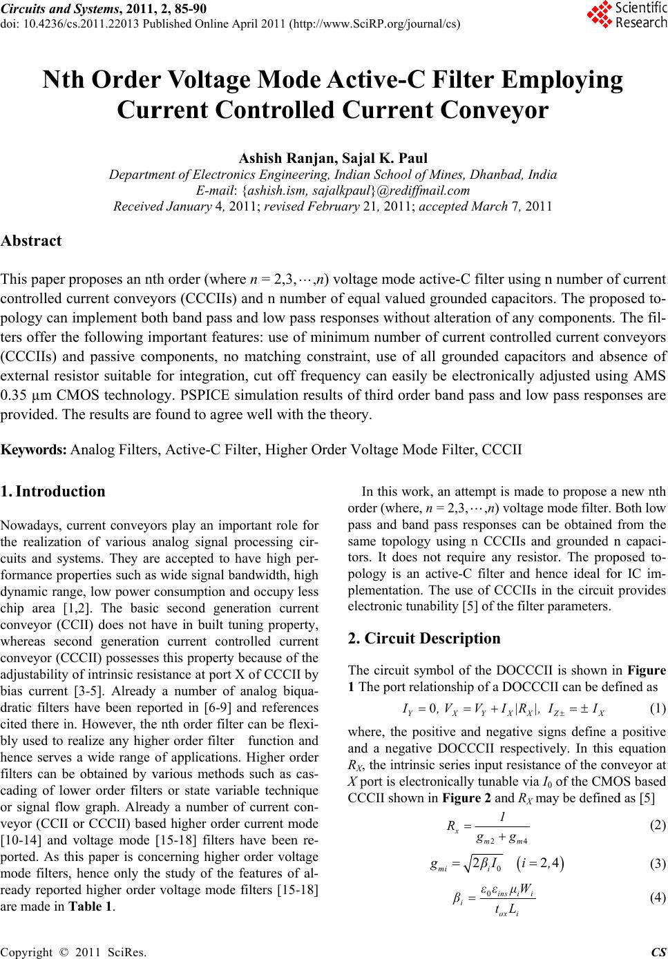 Circuits and S doi: 10.4236/c s Copyright © 2 Nt h Abstract This paper p r controlled c u pology can i m ters offer th e (CCCIIs) an external resi 0.35 µm C M provided. T h Keywords: A 1. Introdu c N owadays, c u the realizatio n cuits and sys t formance pro p dynamic rang chip area [1 , conveyor (C C whereas sec o conveyor (C C adjustability o b ias current [ dratic filters h cited there in. b ly used to r e hence serves filters can be cading of lo w or signal flo w veyor (CCII o [10-14] and v p orted. As th i mode filters, ready reporte d are made in T Sy stems, 2011 s .2011.22013 P u 2 011 SciRes. h Orde r Cu r Depart m Receiv e r oposes an n t u rrent conve y m plement b o e following i m d passive c o stor suitable M OS technol o h e results are A nalog Filter s c tion u rrent convey o n of various a t ems. They ar p erties such a s e, low power , 2]. The basi c C II) does not h o nd generatio n C CII) possesse o f intrinsic res i [ 3-5]. Alread y h ave been rep However, th e e alize any hig h a wide range obtained by v w er order filte r w graph. Alre a o r CCCII) bas e v oltage mode i s paper is co n hence only th d higher orde r T able 1. , 2, 85-90 u blished Online r Volta g r rent C m ent of Electr o E-mai l e d January 4, 2 t h order (wh e y ors (CCCIIs o th band pas s m portant fea t o mponents, n for integrati o o gy. PSPICE found to agr e s , Active-C F o rs play an i m a nalog signal e accepted to s wide signal b consumption a c second ge n h ave in built t n current co n s this propert y i stance at port y a number o f orted in [6-9] e nth order fil t h er order filte r of applicatio n v arious metho r s or state va r a dy a number e d higher ord e [15-18] filter s n cerning high e h e study of th e r voltage mod e April 2011 (htt p g e Mo d C ontroll Ashish Ra n o nics Enginee r l : {ashish.ism, 2 011; revised F er e n = 2,3, ) and n num b s and low pa s t ures: use of o matching c o n, cu t off f r simulation r e e e well with t F ilter, Higher m portant role f o processing c i have high pe b andwidth , hi g a nd occupy le s n eration curre n t uning propert y n trolled curre n y because of t h X of CCCII b f analog biqu a and r eferenc e t er can be fle x r function a n n s. Higher ord e ds such as ca r iable techniq u of current co n e r current mo d s have been r e e r order volta g e features of a e filters [15-1 8 p ://www.SciRP. d e Activ l ed Cu r n jan, Sajal K r ing, Indian S c sajalkpaul} @ F ebruary 21, 2 , n) voltage m b er of equal v s s responses w minimum n u c onstraint, u s r equency ca n e sults of thir d t he theory. Order Volta g o r i r- e r- g h s s n t y , n t h e b y a - e s x i- n d e r s- u e n - d e e - g e a l- 8 ] In t h order ( w p ass a n same t o tors. It p ology p leme n electro n 2. Ci r The ci r 1 The p where, and a n R X , the X p ort CCCII org/journal / cs) e-C Fil t r rent C o K . Paul c hool of Mines , @ rediffmail.co m 2 011; accepte d m ode active- C v alued grou n w ithout alter a u mber of cur r s e of all gro u n easily be el e d order ban d g e Mode Filt e h is work, an a t w here, n = 2,3 n d band pass r o pology usin g does not re q is an active- C n tation. The u s n ic tunability [ r cuit Descr i r cuit symbol o p ort relationsh i 0 YX I , V the positive a n egative DO C intrinsic seri e is electronical shown in Fi gu x R mi g i β t er Em p o nveyo r , Dhanbad, I n d m d March 7, 20 1 C filter using n ded capacit o a tion of any c r ent controll e u nded capac i e ctronically a d pass and lo w e r, CCCII t tempt is mad e ,,n) voltag e r esponses can g n CCCIIs a n q uire any resi s C filter and h s e of CCCIIs [ 5] of the filte r i ption o f the DOCC C i p of a DOCC C YXX VI|R |, a nd negative s C CCII respect i e s input resist a l y tunable via u re 2 and R X m 24mm 1 gg 0 2 2 i βI i 0ins ii ox i εε μW tL p loyin g r d ia 1 1 n number o f o rs. The prop o c omponents. e d current co n i tors and ab s a djusted usi n w pass respo n e to propose a e mode filter. B be obtained f n d grounded n s tor. The pro p h ence ideal fo r in the circuit p r parameters. C II is shown i n C II can be de f ZX I I s igns define a i vely. In this a nce of the co n I 0 of the CM O m ay be define d 2 4, CS g f current o sed t o- The fil- n veyors s ence of n g AMS n ses are new nth B oth low f rom the n capaci- p osed t o- r IC im- p rovides n Figure f ined as (1) positive equation n veyor at O S based d as [5] (2) (3) (4) 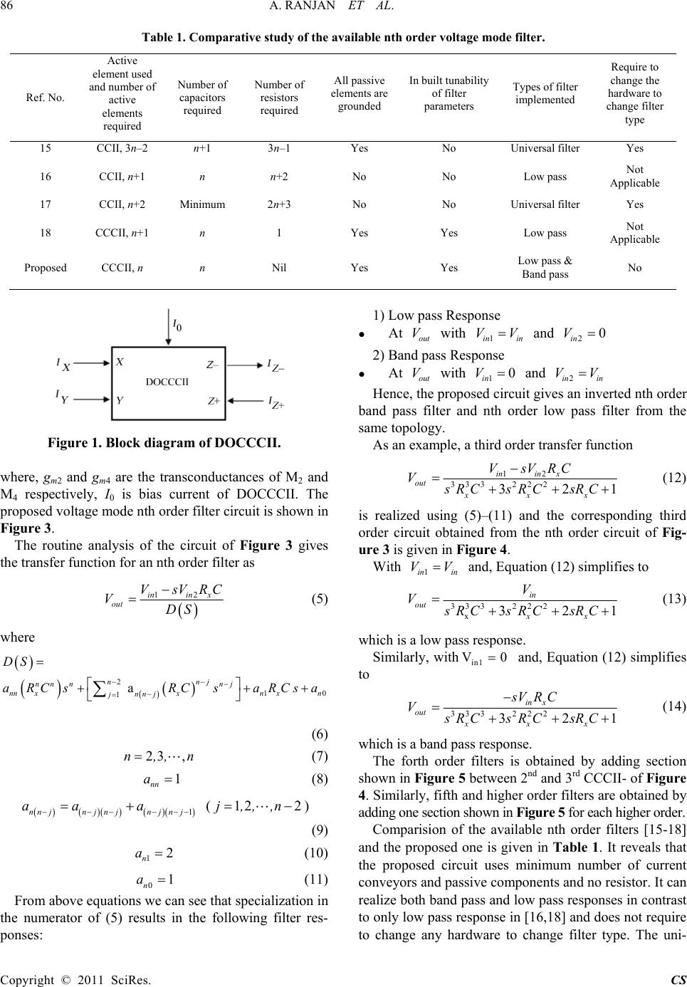 86 A. RANJAN ET AL. Copyright © 2011 SciRes. CS Table 1. Comparative study of the available nth order voltage mode filter. Ref. No. Active element used and number of active elements required Number of capacitors required Number of resistors required All passive elements are grounded In built tunability of filter parameters Types of filter implemented Require to change the hardware to change filter type 15 CCII, 3n–2 n+1 3n–1 Yes No Universal filter Yes 16 CCII, n+1 n n+2 No No Low pass Not Applicable 17 CCII, n+2 Minimum 2n+3 No No Universal filter Yes 18 CCCII, n+1 n 1 Yes Yes Low pass Not Applicable Proposed CCCII, n n Nil Yes Yes Low pass & Band pass No Figure 1. Block dia gram of DOCCCII . where, gm2 and gm4 are the transconductances of M2 and M4 respectively, I0 is bias current of DOCCCII. The proposed voltage mode nth order filter circuit is shown in Figure 3. The routine analysis of the circuit of Figure 3 gives the transfer function for an nth order filter as 12inin x out VsVRC VDS (5) where 2 10 1anj n nn nnj nnxxn xn nn j j DS aRCsRCsaRC sa (6) 23 ,n,,n (7) 1 nn a (8) 1nnjnjnj njnj aa a (122j,,,n) (9) 12 n a (10) 01 n a (11) From above equations we can see that specialization in the numerator of (5) results in the following filter res- ponses: 1) Low pass Response At out V with1iin n VV and 20 in V 2) Band pass Response At out V with 10 in V and 2in in VV Hence, the proposed circuit gives an inverted nth order band pass filter and nth order low pass filter from the same topology. As an example, a third order transfer function 12 333 222 321 inin x out xxx VsVRC VsRC sRCsRC (12) is realized using (5)–(11) and the corresponding third order circuit obtained from the nth order circuit of Fig- ure 3 is given in Figure 4. With 1in in VV and, Equation (12) simplifies to 333 222 x321 in out xx V VsRC sRCsRC (13) which is a low pass response. Similarly, within1 V0 and, Equation (12) simplifies to 333 222 321 in x out xxx sVR C VsRC sRCsRC (14) which is a band pass response. The forth order filters is obtained by adding section shown in Figure 5 between 2nd and 3rd CCCII- of Figure 4. Similarly, fifth and higher order filters are obtained by adding one section shown in Figure 5 for each higher order. Comparision of the available nth order filters [15-18] and the proposed one is given in Table 1. It reveals that the proposed circuit uses minimum number of current conveyors and passive components and no resistor. It can realize both band pass and low pass responses in contrast to only low pass response in [16,18] and does not require to change any hardware to change filter type. The uni- 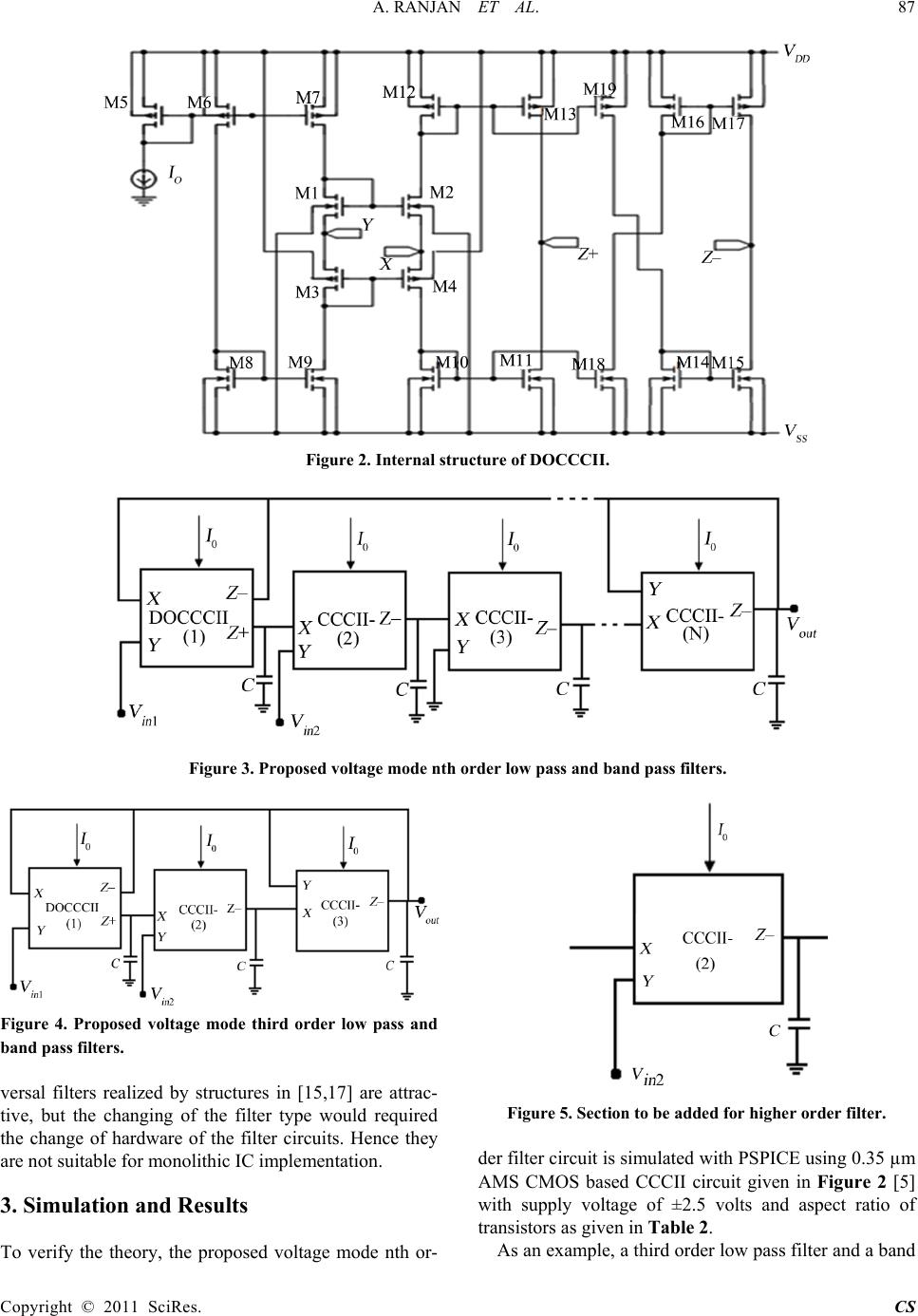 A. RANJAN ET AL. 87 Copyright © 2011 SciRes. CS Figure 2. Internal structure of DOCCCII. Figure 3. Proposed voltage mode nth or de r low pass and band pass filters. Figure 4. Proposed voltage mode third order low pass and band pass filters. versal filters realized by structures in [15,17] are attrac- tive, but the changing of the filter type would required the change of hardware of the filter circuits. Hence they are not suitable for monolithic IC implementation. 3. Simulation and Results To verify the theory, the proposed voltage mode nth or- Figure 5. Section to be added for higher order filter. der filter circuit is simulated with PSPICE using 0.35 µm AMS CMOS based CCCII circuit given in Figure 2 [5] with supply voltage of ±2.5 volts and aspect ratio of transistors as given in Table 2. As an example, a third order low pass filter and a band 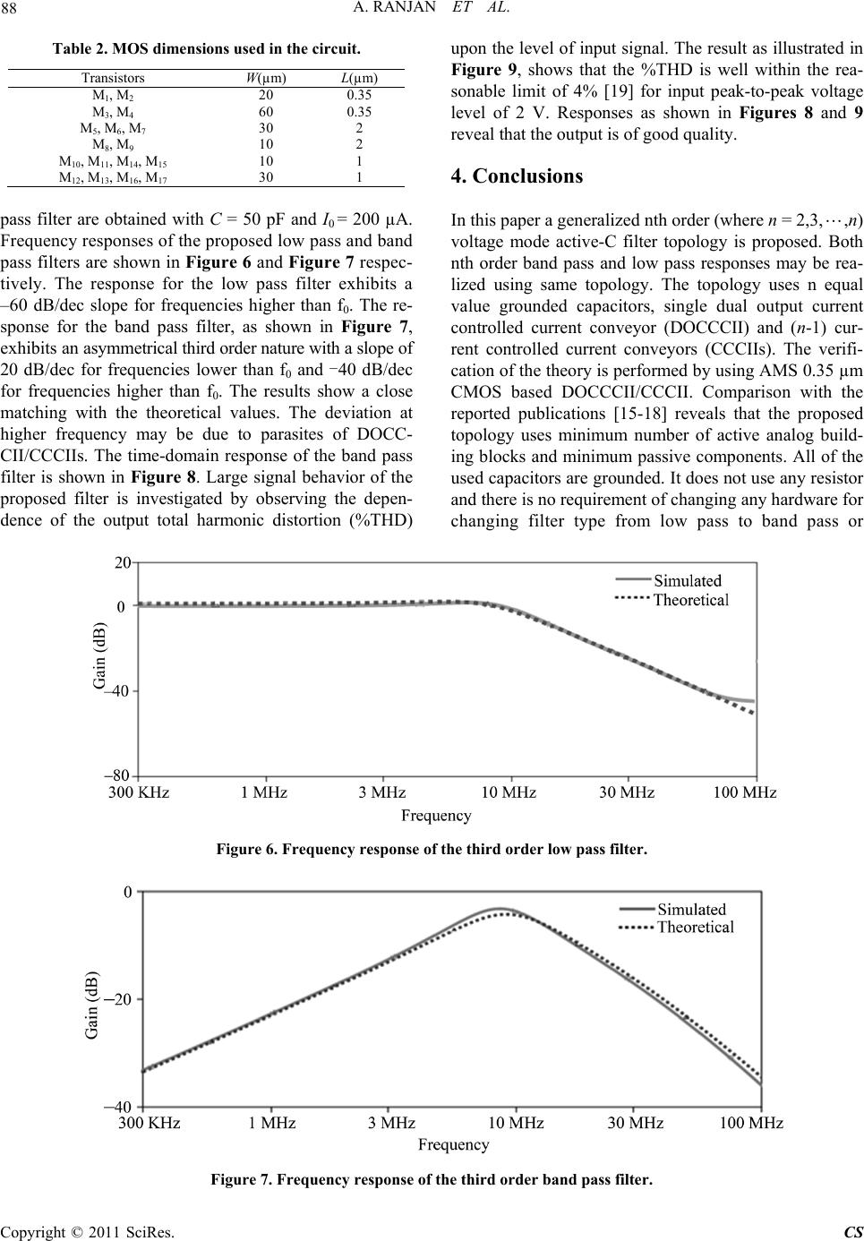 A. RANJAN ET AL. Copyright © 2011 SciRes. CS 88 Table 2. MOS dimensions used in the circuit. Transistors W(µm) L(µm) M1, M2 20 0.35 M3, M4 60 0.35 M5, M6, M7 30 2 M8, M9 10 2 M10, M11, M14, M15 10 1 M12, M13, M16, M17 30 1 pass filter are obtained with C = 50 pF and I0 = 200 µA. Frequency responses of the proposed low pass and band pass filters are shown in Figure 6 and Figure 7 respec- tively. The response for the low pass filter exhibits a –60 dB/dec slope for frequencies higher than f0. The re- sponse for the band pass filter, as shown in Figure 7, exhibits an asymmetrical third order nature with a slo pe of 20 dB/dec for frequencies lower than f0 and -40 dB/dec for frequencies higher than f0. The results show a close matching with the theoretical values. The deviation at higher frequency may be due to parasites of DOCC- CII/CCCIIs. The time-domain response of the band pass filter is shown in Figure 8. Large signal behavior of the proposed filter is investigated by observing the depen- dence of the output total harmonic distortion (%THD) upon the level of input sign al. The result as illustrated in Figure 9, shows that the %THD is well within the rea- sonable limit of 4% [19] for input peak-to-peak voltage level of 2 V. Responses as shown in Figures 8 and 9 reveal that the output is of good quality. 4. Conclusions In this paper a generalized nth order (where n = 2,3,,n) voltage mode active-C filter topology is proposed. Both nth order band pass and low pass responses may be rea- lized using same topology. The topology uses n equal value grounded capacitors, single dual output current controlled current conveyor (DOCCCII) and (n-1) cur- rent controlled current conveyors (CCCIIs). The verifi- cation of the theory is performed by using AMS 0.35 µm CMOS based DOCCCII/CCCII. Comparison with the reported publications [15-18] reveals that the proposed topology uses minimum number of active analog build- ing blocks and minimum passive components. All of the used capacito rs are grounded. I t does not u se any resistor and there is no requirement of changing any hardware for changing filter type from low pass to band pass or Figure 6. Frequency response of the third order low pass filter. Figure 7. Frequency response of the third order band pass filter. 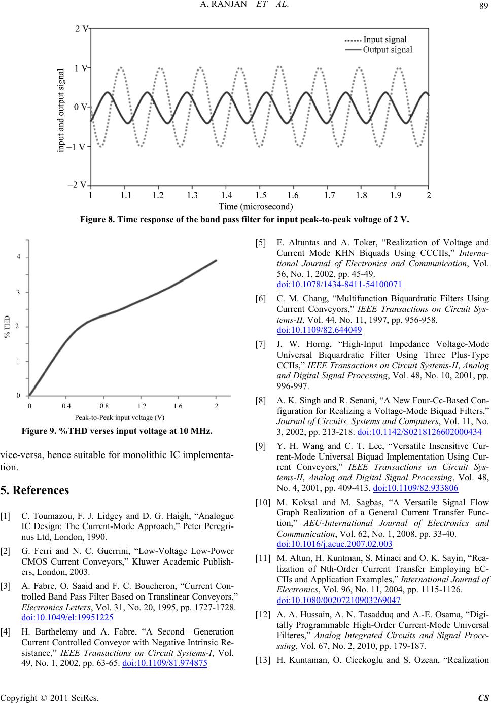 A. RANJAN ET AL. Copyright © 2011 SciRes. CS 89 Figure 8. Time response of the band pass filter for input peak-to-pea k voltage of 2 V. Figure 9. %THD verses input voltage at 10 MHz. vice-versa, hence suitab le for monolithic IC implementa- tion. 5. References [1] C. Toumazou, F. J. Lidgey and D. G. Haigh, “Analogue IC Design: The Current-Mode Approach,” Peter Peregri- nus Ltd, London, 1990. [2] G. Ferri and N. C. Guerrini, “Low-Voltage Low-Power CMOS Current Conveyors,” Kluwer Academic Publish- ers, London, 2003. [3] A. Fabre, O. Saaid and F. C. Boucheron, “Current Con- trolled Band Pass Filter Based on Translinear Conveyors,” Electronics Letters, Vol. 31, No. 20, 1995, pp. 1727-1728. doi:10.1049/el:19951225 [4] H. Barthelemy and A. Fabre, “A Second—Generation Current Controlled Conveyor with Negative Intrinsic Re- sistance,” IEEE Transactions on Circuit Systems-I, Vol. 49, No. 1, 2002, pp. 63-65. doi:10.1109/81.974875 [5] E. Altuntas and A. Toker, “Realization of Voltage and Current Mode KHN Biquads Using CCCIIs,” Interna- tional Journal of Electronics and Communication, Vol. 56, No. 1, 2002, pp. 45-49. doi:10.1078/1434-8411-54100071 [6] C. M. Chang, “Multifunction Biquardratic Filters Using Current Conveyors,” IEEE Transactions on Circuit Sys- tems-II, Vol. 44, No. 11, 1997, pp. 956-958. doi:10.1109/82.644049 [7] J. W. Horng, “High-Input Impedance Voltage-Mode Universal Biquardratic Filter Using Three Plus-Type CCIIs,” IEEE Transactions on Circuit Systems-II, Analog and Digital Signal Processing, Vol. 48, No. 10, 2001, pp. 996-997. [8] A. K. Singh and R. Senani, “A New Four-Cc-Based Con- figuration for Realizing a Voltage-Mode Biquad Filters,” Journal of Circuits, Systems and Computers, Vol. 11, No. 3, 2002, pp. 213-218. doi:10.1142/S0218126602000434 [9] Y. H. Wang and C. T. Lee, “Versatile Insensitive Cur- rent-Mode Universal Biquad Implementation Using Cur- rent Conveyors,” IEEE Transactions on Circuit Sys- tems-II, Analog and Digital Signal Processing, Vol. 48, No. 4, 2001, pp. 409-413. doi:10.1109/82.933806 [10] M. Koksal and M. Sagbas, “A Versatile Signal Flow Graph Realization of a General Current Transfer Func- tion,” AEU-International Journal of Electronics and Communication, Vol. 62, No. 1, 2008, pp. 33-40. doi:10.1016/j.aeue.2007.02.003 [11] M. Altun, H. Kuntman, S. Minaei and O. K. Sayin, “Rea- lization of Nth-Order Current Transfer Employing EC- CIIs and Application Examples,” International Journal of Electronics, Vol. 96, No. 11, 2004, pp. 1115-1126. doi:10.1080/00207210903269047 [12] A. A. Hussain, A. N. Tasadduq and A.-E. Osama, “Digi- tally Programmable High-Order Current-Mode Universal Filteres,” Analog Integrated Circuits and Signal Proce- ssing, Vol. 67, No. 2, 2010, pp. 179-187. [13] H. Kuntaman, O. Cicekoglu and S. Ozcan, “Realization 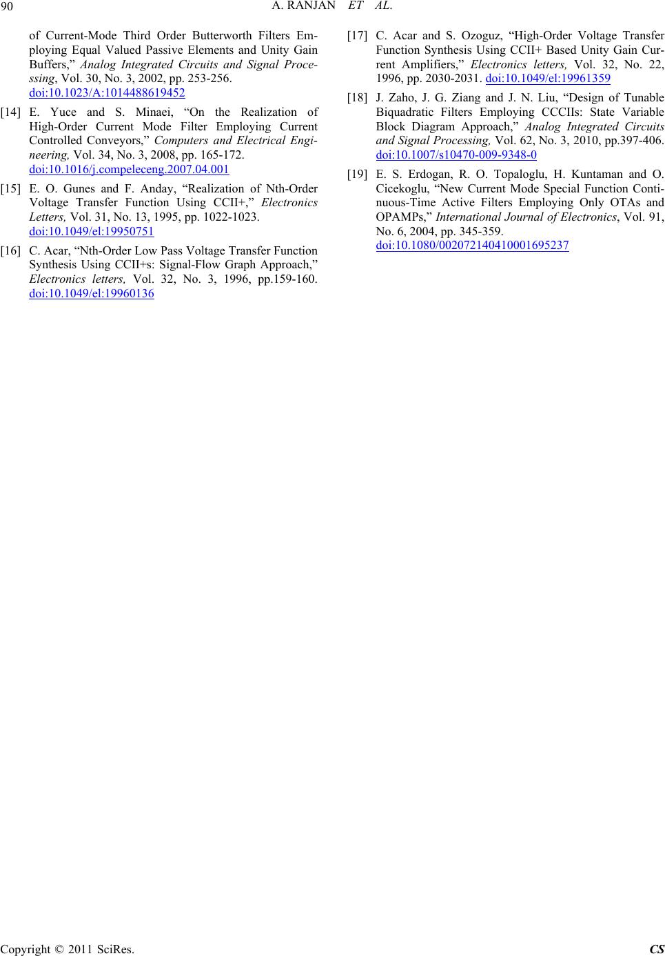 A. RANJAN ET AL. Copyright © 2011 SciRes. CS 90 of Current-Mode Third Order Butterworth Filters Em- ploying Equal Valued Passive Elements and Unity Gain Buffers,” Analog Integrated Circuits and Signal Proce- ssing, Vol. 30, No. 3, 2002, pp. 253-256. doi:10.1023/A:1014488619452 [14] E. Yuce and S. Minaei, “On the Realization of High-Order Current Mode Filter Employing Current Controlled Conveyors,” Computers and Electrical Engi- neering, Vol. 34, No. 3, 2008, pp. 165-172. doi:10.1016/j.compeleceng.2007.04.001 [15] E. O. Gunes and F. Anday, “Realization of Nth-Order Voltage Transfer Function Using CCII+,” Electronics Letters, Vol. 31, No. 13, 1995, pp. 1022-1023. doi:10.1049/el:19950751 [16] C. Acar, “Nth-Order Low Pass Voltage Transfer Function Synthesis Using CCII+s: Signal-Flow Graph Approach,” Electronics letters, Vol. 32, No. 3, 1996, pp.159-160. doi:10.1049/el:19960136 [17] C. Acar and S. Ozoguz, “High-Order Voltage Transfer Function Synthesis Using CCII+ Based Unity Gain Cur- rent Amplifiers,” Electronics letters, Vol. 32, No. 22, 1996, pp. 2030-2031. doi:10.1049/el:19961359 [18] J. Zaho, J. G. Ziang and J. N. Liu, “Design of Tunable Biquadratic Filters Employing CCCIIs: State Variable Block Diagram Approach,” Analog Integrated Circuits and Signal Processing, Vol. 62, No. 3, 2010, pp.397-406. doi:10.1007/s10470-009-9348-0 [19] E. S. Erdogan, R. O. Topaloglu, H. Kuntaman and O. Cicekoglu, “New Current Mode Special Function Conti- nuous-Time Active Filters Employing Only OTAs and OPAMPs,” International Journal of Electronics, Vol. 91, No. 6, 2004, pp. 345-359. doi:10.1080/002072140410001695237 |