Paper Menu >>
Journal Menu >>
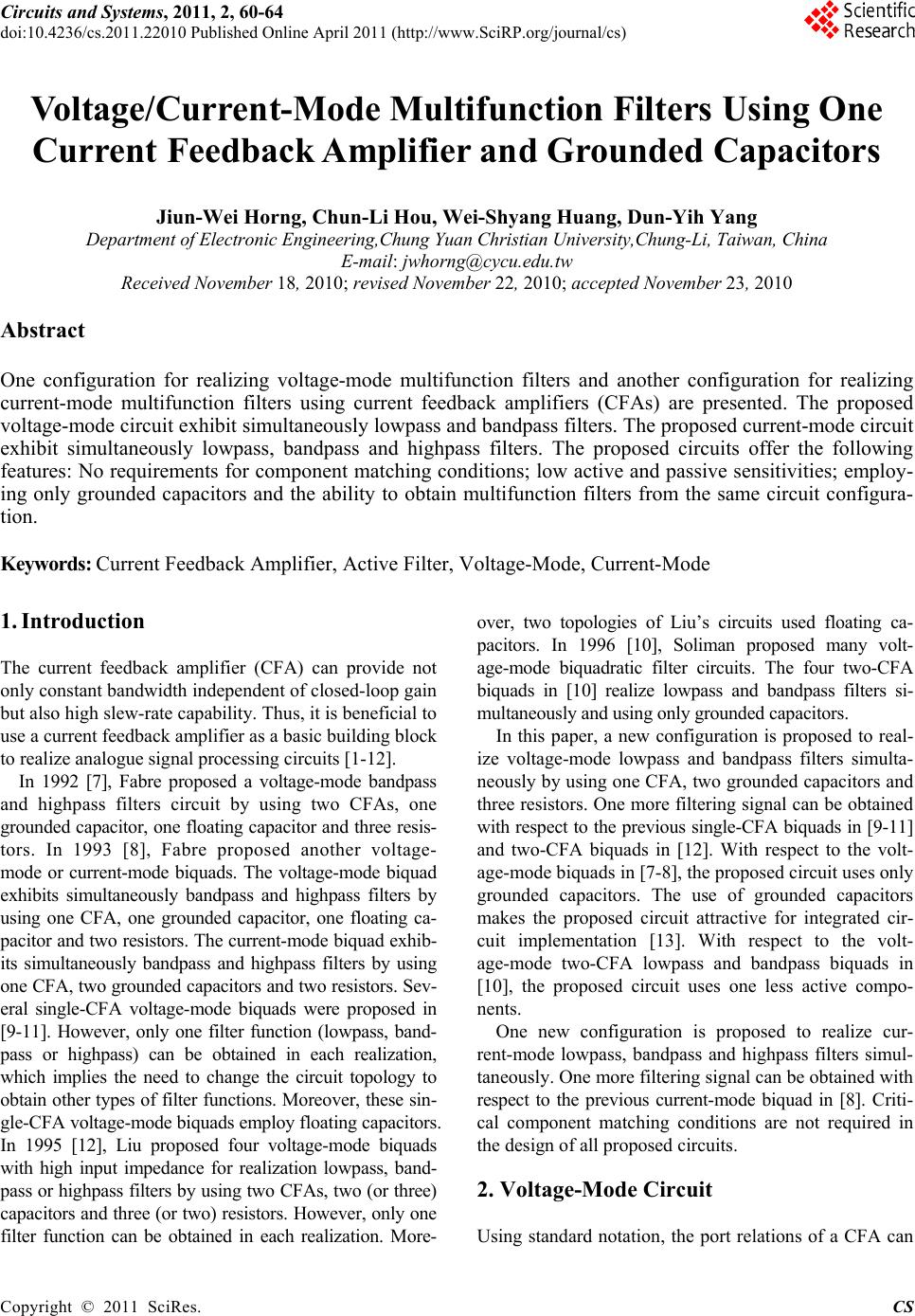 Circuits and Systems, 2011, 2, 60-64 doi:10.4236/cs.2011.22010 Published Online April 2011 (http://www.SciRP.org/journal/cs) Copyright © 2011 SciRes. CS Voltage/Current-Mode Multifunction Filters Using One Current Feedback Amplifier and Grounded Capacitors Jiun-Wei Horng, Chun-Li Hou, Wei-Shyang Huang, Dun-Yih Yang Department of El ect roni c Engi neeri ng,C hu n g Yuan Christian Universi t y ,C hun g-Li, Taiwan, China E-mail: jwhorng@cycu.edu.tw Received November 18, 2010; revised November 22, 2010; accepted November 23, 2010 Abstract One configuration for realizing voltage-mode multifunction filters and another configuration for realizing current-mode multifunction filters using current feedback amplifiers (CFAs) are presented. The proposed voltage-mode circuit exhibit simultaneously lowpass and bandpass filters. The proposed current-mode circuit exhibit simultaneously lowpass, bandpass and highpass filters. The proposed circuits offer the following features: No requirements for component matching conditions; low active and passive sensitivities; employ- ing only grounded capacitors and the ability to obtain multifunction filters from the same circuit configura- tion. Keywords: Current Feedback Amplifier, Active Filter, Voltage-Mode, Current-Mode 1. Introduction The current feedback amplifier (CFA) can provide not only constant bandwidth independent of closed-loop gain but also high slew-rate capability. Thus, it is ben eficial to use a current feedback amplifier as a basic building block to realize analogue signal processing circuits [1-12]. In 1992 [7], Fabre proposed a voltage-mode bandpass and highpass filters circuit by using two CFAs, one grounded capacitor, one floating capacitor and three resis- tors. In 1993 [8], Fabre proposed another voltage- mode or current-mode biquads. The voltage-mode biquad exhibits simultaneously bandpass and highpass filters by using one CFA, one grounded capacitor, one floating ca- pacitor and two resistors. The current-mode biquad exhib- its simultaneously bandpass and highpass filters by using one CFA, two grounded capacitors and two resistors. Sev- eral single-CFA voltage-mode biquads were proposed in [9-11]. However, only one filter function (lowpass, band- pass or highpass) can be obtained in each realization, which implies the need to change the circuit topology to obtain other types of filter functions. Moreover, these sin- gle-CFA voltage-mode biquads employ floating capacitors. In 1995 [12], Liu proposed four voltage-mode biquads with high input impedance for realization lowpass, band- pass or highpass filters by using two CFAs, two (or three) capacitors and three (or two) resistors. However, only one filter function can be obtained in each realization. More- over, two topologies of Liu’s circuits used floating ca- pacitors. In 1996 [10], Soliman proposed many volt- age-mode biquadratic filter circuits. The four two-CFA biquads in [10] realize lowpass and bandpass filters si- multaneously and using o nly groun ded capacitors. In this paper, a new configuration is proposed to real- ize voltage-mode lowpass and bandpass filters simulta- neously by using on e CFA, two grounded capacitors and three resistors. One more filtering signal can be obtained with respect to the previous single-CFA biquads in [9-11] and two-CFA biquads in [12]. With respect to the volt- age-mode biquads in [7-8], the proposed circuit uses only grounded capacitors. The use of grounded capacitors makes the proposed circuit attractive for integrated cir- cuit implementation [13]. With respect to the volt- age-mode two-CFA lowpass and bandpass biquads in [10], the proposed circuit uses one less active compo- nents. One new configuration is proposed to realize cur- rent-mode lowpass, bandpass and highpass filters simul- taneously. One more filtering sig nal can b e obtained with respect to the previous current-mode biquad in [8]. Criti- cal component matching conditions are not required in the design of all proposed circuits. 2. Voltage-Mode Circuit Using standard notation, the port relations of a CFA can 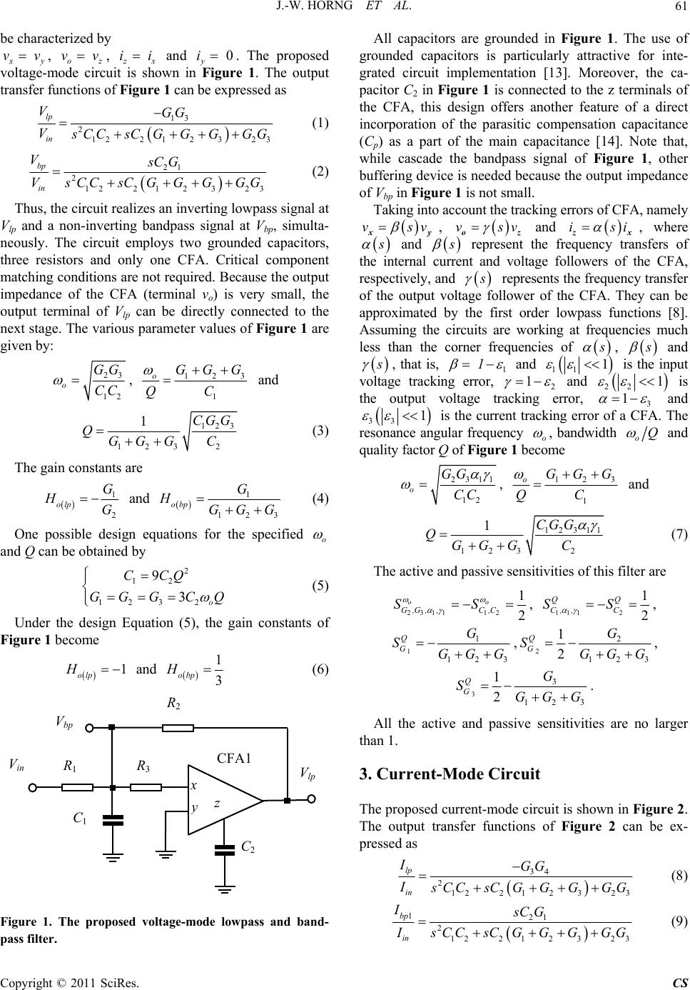 J.-W. HORNG ET AL. Copyright © 2011 SciRes. CS 61 be characterized by x y v v, oz v v, z x i i and 0 y i . The proposed voltage-mode circuit is shown in Figure 1. The output transfer functions of Figure 1 can be expressed as 13 2122 12323 lp in VGG V s CCsC GGGGG (1) 21 2122 12323 bp in VsCG V s CCsC GGGGG (2) Thus, the circuit realizes an inverting lowpass signal at Vlp and a non-inverting bandpass signal at Vbp, simulta- neously. The circuit employs two grounded capacitors, three resistors and only one CFA. Critical component matching conditions are not required. Because the output impedance of the CFA (terminal vo) is very small, the output terminal of Vlp can be directly connected to the next stage. The various parameter values of Figure 1 are given by: 23 12 o GG CC , 123 1 oGGG QC and 123 123 2 1CGG QGGG C (3) The gain constants are 1 2 olp G HG and 1 123 obp G HGGG (4) One possible design equations for the specified o and Q can be obtained by 2 12 123 2 9 3o CCQ GGG CQ (5) Under the design Equation (5), the gain constants of Figure 1 become 1 olp H and 1 3 obp H (6) Figure 1. The proposed voltage-mode lowpass and band- pass filter. All capacitors are grounded in Figure 1. The use of grounded capacitors is particularly attractive for inte- grated circuit implementation [13]. Moreover, the ca- pacitor C2 in Figure 1 is connected to the z terminals of the CFA, this design offers another feature of a direct incorporation of the parasitic compensation capacitance (Cp) as a part of the main capacitance [14]. Note that, while cascade the bandpass signal of Figure 1, other buffering device is needed because the output impedance of Vbp in Figure 1 is not small. Taking into account the tracking errors of CFA, namely vsv xy , vsv oz and isi zx , where s and s represent the frequency transfers of the internal current and voltage followers of the CFA, respectively, and s represents the frequency transfer of the output voltage follower of the CFA. They can be approximated by the first order lowpass functions [8]. Assuming the circuits are working at frequencies much less than the corner frequencies of s , s and s , that is, 1 1 and 11 1 is the input voltage tracking error, 2 1 and 22 1 is the output voltage tracking error, 3 1 and 33 1 is the current tracking error of a CFA. The resonance angular frequency o , bandwidth oQ and quality factor Q of Figure 1 become 2311 12 o GG CC , 123 1 oGGG QC and 12311 123 2 1CGG QGGG C (7) The active and passive sensitivities of this filter are 2311 12 1 2 oo G,G, ,C,C SS , 111 2 1 2 QQ C, ,C SS , 1 1 123 Q G G SGGG ,2 2 123 1 2 Q G G SGGG , 3 3 123 1 2 Q G G SGGG . All the active and passive sensitivities are no larger than 1. 3. Current-Mode Circuit The proposed current- mode circuit is shown in Figure 2. The output transfer functions of Figure 2 can be ex- pressed as 34 2122 12323 lp in IGG I s CCsC GGGGG (8) 121 2122 12323 bp in IsCG I s CCsC GGGGG (9) R 3 x y z R 1 R 2 Vbp C2 Vlp C1 Vin CFA1 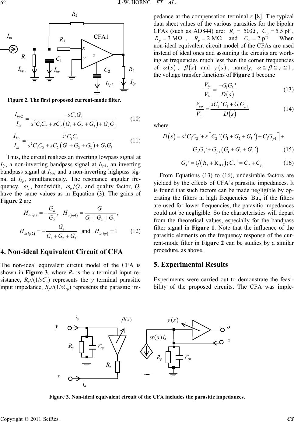 J.-W. HORNG ET AL. Copyright © 2011 SciRes. CS 62 Figure 2. The first proposed current-mode filter. 223 2122 12323 bp in IsCG I s CCsC GGGGG (10) 212 2122 12323 hp in IsCC I s CCsC GGGGG (11) Thus, the circuit realizes an inverting lowpass signal at Ilp, a non-inverting bandpass signal at Ibp1, an inverting bandpass signal at Ibp2 and a non-inverting highpass sig- nal at Ihp, simultaneously. The resonance angular fre- quency, o , bandwidth, oQ , and quality factor, Q, have the same values as in Equation (3). The gains of Figure 2 are 4 2 o( lp ) G HG , 1 1123 obp G HGGG , 3 2123 obp G HGGG and 1 ohp H (12) 4. Non-ideal Equivalent Circuit of CFA The non-ideal equivalent circuit model of the CFA is shown in Figure 3, where Rx is the x terminal input re- sistance, Ry//(1/sCy) represents the y terminal parasitic input impedance, Rp//(1/sCp) represents the parasitic im- pedance at the compensation terminal z [8]. The typical data sheet values of the various parasitics for the bipolar CFAs (such as AD844) are: 50 x R , 55pF p C. , 3M p R , 2M y R and 2pF y C . When non-ideal equivalent circuit model of the CFAs are used instead of ideal ones and assuming the circuits are work- ing at frequencies much less than the corner frequencies of s , s and s , namely, 1 , the voltage transfer functions of Figure 1 become 13 lp in VGG' VDs (13) 21 11bp p in VsC'GGG VDs (14) where 21221231 1p DssCC' sC'GGG'CG 231 123p GG' GGGG' (15) 33X1221 1R; p G'RC' CC (16) From Equations (13) to (16), undesirable factors are yielded by the effects of CFA’s parasitic impedances. It is found that such factors can be made negligible by op- erating the filters in high frequencies. But, if the filters are used for lower frequencies, the parasitic impedances could not be negligible. So the characteristics will depart from the theoretical values, especially for the bandpass filter signal in Figure 1. Note that the influence of the parasitic elements on the frequency response of the cur- rent-mode filter in Figure 2 can be studies by a similar procedure, as above. 5. Experimental Results Experiments were carried out to demonstrate the feasi- bility of the proposed circuits. The CFA was imple- Figure 3. Non-ideal equivalent circuit of the CFA includes the parasitic impedances. R 3 x y z R 1 R 2 I bp1 C2 I hp C1 I in CFA1 I bp2 R 4 I lp )(s )(s Cy R x iy R y Cp ix R p y z x )(s ix o 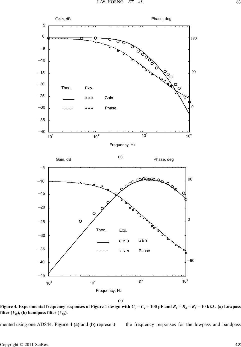 J.-W. HORNG ET AL. Copyright © 2011 SciRes. CS 63 (a) (b) Figure 4. Experimental frequency responses of Figure 1 design with C1 = C2 = 100 pF and R1 = R2 = R3 = 10 k. (a) Lowpass filter (Vlp), (b) bandpass filter (Vbp). mented using one AD844. Figure 4 (a) and (b) represent the frequency responses for the lowpass and bandpass 10 3 10 4 10 5 10 6 – 40 – 35 – 30 – 25 – 20 – 15 – 10 – 5 0 5 0 90 180 Phase, de g Fre q uenc y , Hz Gain, dB Exp. Phase Gain Theo. -.-.-.- x x x o o o 10 3 10 4 10 5 10 6 – 45 – 40 – 35 – 30 – 25 – 20 – 15 – 10 – 5 – 90 0 90 Phase, deg Frequency, Hz Gain, dB Exp. Phase Gain Theo. -.-.-.- x x x o o o  J.-W. HORNG ET AL. Copyright © 2011 SciRes. CS 64 filters of Figure 1, respectively, designed with C1 = C2 = 100 pF and R1 = R2 = R3 = 10 k. Experimental results confirm the theoretical analysis. 6. Conclusions In this paper, a configuration for realizing voltage-mode multifunction filters and a configuration for realizing current-mode multifunction filters using CFAs are pre- sented. The proposed voltage-mode circuit exhibits si- multaneously lowpass and bandpass filters by using one CFA, two grounded capacitors and three resistors. The proposed current-mode circuit exhibit simultaneously lowpass, bandpass and highpass filters by using one CFA, two grounded capacitors and four resistors. The proposed circuits have no requirements for component matching conditions. The active and passive sensitivities are low. 7. References [1] S. S. Gupta, D. R. Bhaskar and R. Senani, “New Voltage Controlled Oscillators Using CFOAs,” International Journal of Electronics and Communications (AEU), Vol. 63, No. 3, 2009, pp. 209-217. doi:10.1016/j.aeue.2008.01.002 [2] E. Yuce, “Novel Lossless and Lossy Grounded Inductor Simulators Consisting of a Canonical Number of Com- ponents,” Analog Integrated Circuits and Signal Proc- essing, Vol. 59, No. 1, 2009, pp. 77-82. doi:10.1007/s10470-008-9235-0 [3] R. Nandi, T. K. Bandyopadhyay, S. K. Sanyal and S. Das, “Selective Filters and Sinusoidal Oscillators Using CFA Transimpedance Pole,” Circuits, Systems and Signal Processing, Vol. 28, No. 3, 2009, pp. 349-359. [4] J. W. Horng, P. Y. Chou and J. Y. Wu, “Volt- age/Current-Mode Multifunction Filters Using Cur- rent-Feedback Amplifiers and Grounded Capacitors,” Ac- tive and Passive Electronic Components, Vol. 2010, 2010, pp. 1-5. doi:10.1155/2010/785631 [5] K. Kumar and K. Pal, “High Input Impedance Voltage Mode Universal Biquad Filter,” Indian Journal of Pure and Applied Physics, Vol. 48, No. 4, 2010, pp. 292-296. [6] N. Nikoloudis and C. Psychalinos, “Multiple Input Single Output Universal Biquad Filter with Current Feedback Operational Amplifiers,” Circuits, Systems and Signal Processing, Vol. 29, No. 6, 2010, pp. 1167-1180. doi:10.1007/s00034-010-9194-4 [7] A. Fabre, “Gyrator Implementation from Commercially Available Transimpedance Operational Amplifiers,” Electronics Letters, Vol. 28, No. 3, 1992, pp. 263-264. doi:10.1049/el:19920162 [8] A. Fabre, “Insensitive Voltage-Mode and Current-Mode Filters from Commercially Available Transimpedance Opamps,” Proceedings of the Institution of Electrical En- gineers, Vol. 140, No. 5, 1993, pp. 319-321. [9] S. I. Liu and Y. S. Hwang, “Realisation of R-L and C-D Impedances Using a Current-Feedback Amplifier and Its Applications,” Electronics Letters, Vol. 30, No. 5, 1994, pp. 380-381. doi:10.1049/el:19940286 [10] A. M. Soliman, “Applications of the Current Feedback Amplifiers,” Analog Integrated Circuits and Signal Processing, Vol. 11, No. 3, 1996, pp. 265-302. doi:10.1007/BF00240490 [11] A. M. Soliman, “A New Filter Configuration Using Cur- rent Feedback Op-Amp,” Microelectronics Journal, Vol. 29, No. 7, 1998, pp. 409-419. doi:10.1016/S0026-2692(97)00025-6 [12] S. I. Liu, “High Input Impedance Filters with Low Com- ponent Spread Using Current-Feedback Amplifiers,” Electronic s Letters, Vol. 31, No. 13, 1995, pp. 1042-1043. doi:10.1049/el:19950725 [13] M. Bhushan and R. W. Newcomb, “Grounding of Ca- pacitors in Integrated Circuits,” Electronic Letters, Vol. 3, No. 4, 1967, pp. 148-149. doi:10.1049/el:19670114 [14] R. Senani, “Realization of a Class of Analog Signal Processing/Signal Generation Circuits: Novel Configura- tions Using Current Feedback Op-Amps,” Frequenz, Vol. 52, No. 9-10, 1998, pp. 196-206. doi:10.1515/FREQ.1998.52.9-10.196 |