Paper Menu >>
Journal Menu >>
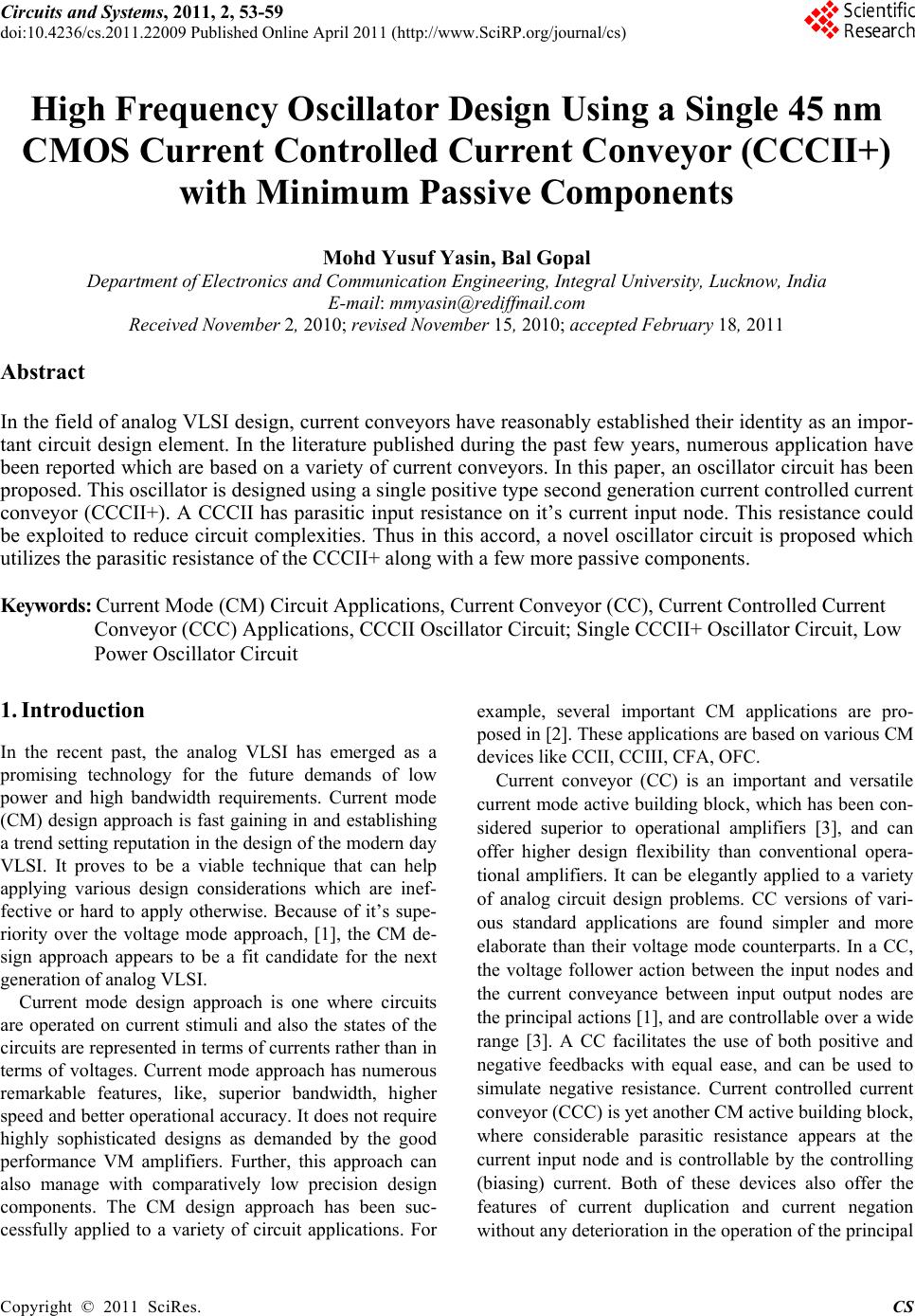 Circuits and Systems, 2011, 2, 53-59 doi:10.4236/cs.2011.22009 Published Online April 2011 (http://www.SciRP.org/journal/cs) Copyright © 2011 SciRes. CS High Frequency Oscillator Design Using a Single 45 nm CMOS Current Controlled Current Conveyor (CCCII+) with Minimum Passive Components Mohd Yusuf Yasin, Bal Gopal Department of Electronics and Communication Engineering, Integral University, Lucknow, India E-mail: mmyasin@rediffmail.com Received November 2, 2010; revised November 15, 2010; accepted February 18, 2011 Abstract In the field of analog VLSI design, current conveyors have reasonably established their identity as an impor- tant circuit design element. In the literature published during the past few years, numerous application have been reported which are based on a variety of current conveyors. In this paper, an oscillator circuit has been proposed. This oscillator is designed using a single positive type second generation current controlled current conveyor (CCCII+). A CCCII has parasitic input resistance on it’s current input node. This resistance could be exploited to reduce circuit complexities. Thus in this accord, a novel oscillator circuit is proposed which utilizes the parasitic resistance of the CCCII+ along with a few more passive components. Keywords: Current Mode (CM) Circuit Applications, Current Conveyor (CC), Current Controlled Current Conveyor (CCC) Applications, CCCII Oscillator Circuit; Single CCCII+ Oscillator Circuit, Low Power Oscillator Circuit 1. Introduction In the recent past, the analog VLSI has emerged as a promising technology for the future demands of low power and high bandwidth requirements. Current mode (CM) design approach is fast gaining in and establishing a trend setting reputation in the design of the modern day VLSI. It proves to be a viable technique that can help applying various design considerations which are inef- fective or hard to apply otherwise. Because of it’s supe- riority over the voltage mode approach, [1], the CM de- sign approach appears to be a fit candidate for the next generation of analog VLSI. Current mode design approach is one where circuits are operated on current stimuli and also the states of the circuits are represented in terms of currents rather than in terms of voltages. Current mode approach has numerous remarkable features, like, superior bandwidth, higher speed and better operational accuracy. It does not require highly sophisticated designs as demanded by the good performance VM amplifiers. Further, this approach can also manage with comparatively low precision design components. The CM design approach has been suc- cessfully applied to a variety of circuit applications. For example, several important CM applications are pro- posed in [2]. These applications are based on various CM devices like CCII, CCIII, CFA, OFC. Current conveyor (CC) is an important and versatile current mode active building block, which has been con- sidered superior to operational amplifiers [3], and can offer higher design flexibility than conventional opera- tional amplifiers. It can be elegantly applied to a variety of analog circuit design problems. CC versions of vari- ous standard applications are found simpler and more elaborate than their voltage mode counterparts. In a CC, the voltage follower action between the input nodes and the current conveyance between input output nodes are the principal actions [1], and are controllable over a wide range [3]. A CC facilitates the use of both positive and negative feedbacks with equal ease, and can be used to simulate negative resistance. Current controlled current conveyor (CCC) is yet another CM active building block, where considerable parasitic resistance appears at the current input node and is controllable by the controlling (biasing) current. Both of these devices also offer the features of current duplication and current negation without any deterioration in the operation of the principal 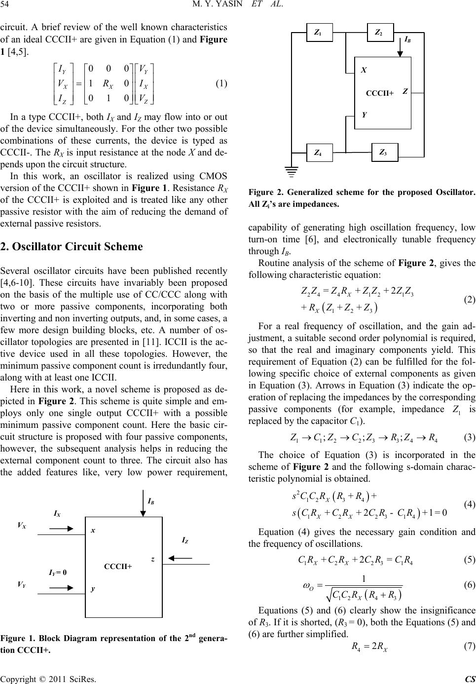 M. Y. YASIN ET AL. Copyright © 2011 SciRes. CS 54 circuit. A brief review of the well known characteristics of an ideal CCCII+ are given in Equation (1) and Figure 1 [4,5]. 000 10 010 YY XXX Z Z IV VRI V I (1) In a type CCCII+, both IX and IZ may flow into or out of the device simultaneously. For the other two possible combinations of these currents, the device is typed as CCCII-. The RX is input resistance at the node X and de- pends upon the circuit structure. In this work, an oscillator is realized using CMOS version of the CCCII+ shown in Figure 1. Resistance RX of the CCCII+ is exploited and is treated like any other passive resistor with the aim of reducing the demand of external passive resistors. 2. Oscillator Circuit Scheme Several oscillator circuits have been published recently [4,6-10]. These circuits have invariably been proposed on the basis of the multiple use of CC/CCC along with two or more passive components, incorporating both inverting and non inverting outputs, and, in some cases, a few more design building blocks, etc. A number of os- cillator topologies are presented in [11]. ICCII is the ac- tive device used in all these topologies. However, the minimum passive component count is irredundantly four, along with at least one ICCII. Here in this work, a novel scheme is proposed as de- picted in Figure 2. This scheme is quite simple and em- ploys only one single output CCCII+ with a possible minimum passive component count. Here the basic cir- cuit structure is proposed with four passive components, however, the subsequent analysis helps in reducing the external component count to three. The circuit also has the added features like, very low power requirement, Figure 1. Block Diagram representation of the 2nd genera- tion CCCII+. Figure 2. Generalized scheme for the proposed Oscillator. All Zi’s are impedances. capability of generating high oscillation frequency, low turn-on time [6], and electronically tunable frequency through IB. Routine analysis of the scheme of Figure 2, gives the following characteristic equation: 24 41213 123 = + + 2 + ++ X X Z ZZRZZZZ RZZ Z (2) For a real frequency of oscillation, and the gain ad- justment, a suitable second order polynomial is required, so that the real and imaginary components yield. This requirement of Equation (2) can be fulfilled for the fol- lowing specific choice of external components as given in Equation (3). Arrows in Equation (3) indicate the op- eration of replacing the impedances by the corresponding passive components (for example, impedance 1 Z is replaced by the capacitor C1). 112 2334 4 ; ;; Z CZ CZRZR (3) The choice of Equation (3) is incorporated in the scheme of Figure 2 and the following s-domain charac- teristic polynomial is obtained. 2 123 4 12 2314 + + + + 2- + 1 = 0 X XX sCCR RR sCRCRCR CR (4) Equation (4) gives the necessary gain condition and the frequency of oscillations. 12 2314 ++2= XX CRCRCRCR (5) 124 3 1 O X CC RRR (6) Equations (5) and (6) clearly show the insignificance of R3. If it is shorted, (R3 = 0), both the Equations (5) and (6) are further simplified. 42X RR (7) x y z IX IY = 0 IZ VX VY CCCII+ IB Z1 Z4 Z2 Z3 X Y Z CCCII+ IB 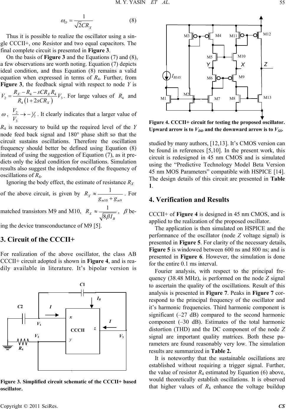 M. Y. YASIN ET AL. Copyright © 2011 SciRes. CS 55 1 2 O X CR (8) Thus it is possible to realize the oscillator using a sin- gle CCCII+, one Resistor and two equal capacitors. The final complete circuit is presented in Figure 3. On the basis of Figure 3 and the Equations (7) and (8), a few observations are worth noting. Equation (7) depicts ideal condition, and thus Equation (8) remains a valid equation when expressed in terms of R4. Further, from Figure 3, the feedback signal with respect to node Y is 44 23 412 XX X RRsCRR VV RsCR . For large values of 4 R and , 212 3 V V . It clearly indicates that a larger value of R4 is necessary to build up the required level of the Y node feed back signal and 180 phase shift so that the circuit sustains oscillations. Therefore the oscillation frequency should better be defined using Equation (8) instead of using the suggestion of Equation (7), as it pre- dicts only the ideal condition for oscillations. Simulation results also suggest the independence of the frequency of oscillations of R4. Ignoring the body effect, the estimate of resistance RX of the above circuit, is given by 10 9 1 Xmm R g g . For matched transistors M9 and M10, 1 8 X B R I , be- ing the device transconductance of M9 [5]. 3. Circuit of the CCCII+ For realization of the above oscillator, the class AB CCCII+ circuit adopted is shown in Figure 4, and is rea- dily available in literature. It’s bipolar version is Figure 3. Simplified circuit schematic of the CCCII+ based oscillator. Figure 4. CCCII+ circuit for testing the proposed oscillator. Upward arrow is to VDD and the downward arrow is to VSS. studied by many authors, [12,13]. It’s CMOS version can be found in references [5,10]. In the present work, this circuit is redesigned in 45 nm CMOS and is simulated using the “Predictive Technology Model Beta Version 45 nm MOS Parameters” compatible with HSPICE [14]. The design details of this circuit are presented in Table 1. 4. Verification and Results CCCII+ of Figure 4 is designed in 45 nm CMOS, and is applied to the realization of the proposed oscillator. The application is then simulated on HSPICE and the performance of the oscillator (node Z voltage signal) is presented in Figure 5. For clarity of the necessary details, Figure 5 is windowed between 600 ns and 800 ns; and is presented in Figure 6. However, the simulation is done for the entire 0.1 ms interval. Fourier analysis, with respect to the principal fre- quency (38.48 MHz), is performed on the node Z signal to ascertain the quality of the oscillations. Result of this analysis is presented in Figure 7. Peaks in Figure 7 cor- respond to the principal frequency of the oscillator and it’s harmonic frequencies. Third harmonic component is significant (–27 dB) compared to the second harmonic component (–30 dB). Estimates of the total harmonic distortion (THD) and the DC component of the node Z signal are important quality matrices. Both these pa- rameters are found reasonably very low. The simulation results are summarized in Table 2. It is noteworthy that the sustainable oscillations are established without requiring a trigger signal. Further, the value of resistor R4 estimated by Equation (6) above, would theoretically establish oscillations. It is observed that higher values of R4 enhance the voltage buildup C1 I I R4 IB CCCII V3 V1 V2 x y z C2 X YZ IBIAS M2 M6 M7 M3 M4 M5 M10 M9 M11 M12 M1 M8 M13 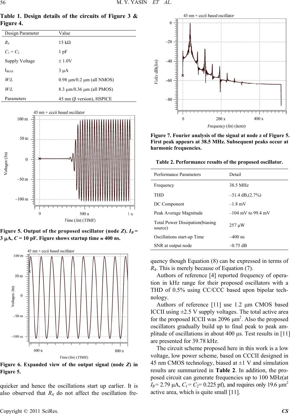 M. Y. YASIN ET AL. Copyright © 2011 SciRes. CS 56 Table 1. Design details of the circuits of Figure 3 & Figure 4. Design Parameter Value R4 15 kΩ C1 = C2 1 pF Supply Voltage 1.0V IBIAS 3 A W/L 0.98 m/0.2 m (all NMOS) W/L 8.3 m/0.36 m (all PMOS) Parameters 45 nm ( version), HSPICE Figure 5. Output of the proposed oscillator (node Z). IB = 3 A, C = 10 pF. Figure shows startup time 400 ns. Figure 6. Expanded view of the output signal (node Z) in Figure 5. quicker and hence the oscillations start up earlier. It is also observed that R4 do not affect the oscillation fre- Figure 7. Fourier analysis of the signal at node z of Figure 5. First peak appears at 38.5 MHz. Subse quent peaks occur at harmonic frequencies. Table 2. Performance results of the proposed oscillator. Performance Parameters Detail Frequency 38.5 MHz THD –31.4 dB,(2.7%) DC Component –1.8 mV Peak Average Magnitude –104 mV to 99.4 mV Total Power Dissipation(biasing source) 257 μW Oscillations start-up Time ~400 ns SNR at output node –0.75 dB quency though Equation (8) can be expressed in terms of R4. This is merely because of Equation (7). Authors of reference [4] reported frequency of opera- tion in kHz range for their proposed oscillators with a THD of 0.5% using CC/CCC based upon bipolar tech- nology. Authors of reference [11] use 1.2 μm CMOS based ICCII using ±2.5 V supply voltages. The total active area for the proposed ICCII was 2096 μm2. Also the proposed oscillators gradually build up to final peak to peak am- plitude of oscillations in about 400 μs. Test results in [11] are presented for 39.78 kHz. The circuit scheme proposed here in this work is a low voltage, low power scheme, based on CCCII designed in 45 nm CMOS technology, biased at ±1 V and simulation results are summarized in Table 2. In addition, the pro- posed circuit can generate frequencies up to 100 MHz(at IB = 2.79 A, C1 = C2= 0.225 pf), and requires only 19.6 μm2 active area, which is quite small [11]. Volts dB(lin)  M. Y. YASIN ET AL. Copyright © 2011 SciRes. CS 57 Figure 8 shows a logarithmic plot for frequency varia- tion with respect to capacitance. The graph shows a nat- ural trend of as frequency drops with increasing capaci- tance. In Figures 9 a plot for frequency variation with bias- ing current of the CCCII+ is presented on logarithmic scale. Simulation results show that a variation in the bias current, IB = 2.9 A (0.4 A to 3.3 A), cause the os- cillator frequency to vary as f = 25.78 MHz (15.2 MHz to 40.98 MHz). For the sake of analysis, a figure of merit could be defined as the current to frequency transfer co- efficient, Kfi, [15]. Thus for C1 = C2 = 1 pf, KfiN = 25.78 MHz /2.9 A = 8.9 MHz/A. Kf-I depends on capacitances and the biasing current. It varies directly with the IB and in- versely with the capacitances. 5. Non Idealities of CCCII+ and Their Impact on Circuit Performance In the above analysis, the CCCII+ is considered ideal. However, a number of non-idealities are present in a practical CCCII+. Considering some of these non- idealities, the device model of the CCCII+ of Figure 1 can be described as below: Z X I I (9) XXX Y VIR V (10) = Y I I (11) where in Equation (9), is the current conveyance coef- ficient between nodes X and Z; in Equation (10), is the voltage gain from node Y to node X and is usuall y < 1. I in Equation (11) is the input current at node Y. For analytical simplicity in the proposed oscillator scheme, it is assumed that this current is a function of the voltage at node Z. Therefore, I = VZ/R , where R is the corre- Figure 8. Frequency variation with Capacitor (C1 = C2 = C). Figure 9. Frequency variation with biasing current. Case 2 : C = 1 pF. sponding resistance at the Y node. Also, as usual, C1 = C2 = C. Using these assumptions, analysis of circuit in Fig- ure 3, gives the following modified characteristic equa- tion: 22 4 4 444 4 4 22 2 10 X XX X sCRR R sCRRRRR RR R R (12) On solving Equation (12), the results are: 4 12 1 11 22 XX K RR RR (13) 24 222 11 2 XX RR K CR CR (14) 1 2O X KK CR (15) 1 O K (16) Equation (13) relates R4, RX, and R . Equation (15) shows a possible elimination of R , Hence either of R4 and RX or both may get modified on account of the volt- age and current tracking errors of the CCCII. Here it is assumed that the circuit non-idealities do not cause sig- nificant change in the value of RX. Equation (16) shows that the oscillation frequency under non-ideal condi- tions is lesser than the ideal oscillation frequency o . Further more, 12 1K (17)  M. Y. YASIN ET AL. Copyright © 2011 SciRes. CS 58 Equation (17) indicates that the variation in the oscil- lator frequency depends on the current and voltage tracking errors, and shows no effect of the current exist- ing at node Y of the CCCII+. Percent decrease in the frequency can be described as: 1 O O K (18) For an ideal situation, 1, 1, I =0 and R ; hence Equation (13) reduces to 4 11 2X RR , and Equa- tion (14) reduces to Equation (8), and hence from Equa- tions (16) and (18), O . But for a 5% tracking error in the values of , and , e.g. = 0.95, = 0.95, using Equation (18), the deviation in the oscillation frequency is observed to be 0 1028 O O . , or 10.3% . 6. Time Domain and Stabilty Considerations The time domain analysis may be significant in giving better insight in the functioning and performance of the oscillator circuit. Assuming the circuit of Figure 3 re- laxed, it can be described by the following system of equations for 1 vt and 3 vt voltages of nodes 1 and 3 respectively 2 211 441 220 XXXX dv dv CRRCRRRR v dt dt (19) 2 233 44 2 3 2 0 XXX X dv tdv t CRRCRR Rdt dt Rv t (20) Equation (19) predicts oscillatory behaviour for the option 42 x RR as has already been indicated above. Using this option, and defining 4 1 o 'CR , general so- lutions of Equations (19) and (20) are as follows 11 2 '' oo j tjt vt cece (21) 22 33 4 '' oo tt vt cece (22) In the above Equations (21) and (22), the coefficients C1, C2, C3, and C4, are arbitrary constants. Equation (21) is oscillatory in nature. In Equation (22), one of the terms rises exponentially to saturation while the other term sharply decays out for large o ' and hence oscillations attain their amplitude. 2 oo ' Again one can consider the gain limits of the circuit. For this purpose, feedback signal from node Z to node X is through C1 and C2 (C1 = C2), while to node Y is through R4. Thus the gain function corresponding to the capacitive feedback arm is: 14 1 2 3 4 1 2 2 1 1 21 2 X X o o s vs s CR CR vs sCRsCR s' s' (23) 222 111 22 222 3 44 1 on on ' vs vs ' (24) Similarly the gain function corresponding to the resis- tive arm is 34 1 4 2 1 1 X XX s vssCR RCR vssCRRRR sCR 2o o s ' s ' (25) 222 3 22 2 1 44 1 on on ' vs vs ' (26) Equations (24) and (26) are described as a function of normalized frequency, no ' . From Equation (24), the gain limits are: for 0 n , 1 3 1 vs vs and n , 11 2 3 vs vs. Similarly from Equation (26), 0 n , 3 1 2 vs vs and n , 3 1 1 vs vs. In both cases, the gain transitions occur between 12 n . However, the phases for Equations (23) and (25), being opposite to one another, start at 0 phase angle, both attain a peak ( 14 1947 n., . and then gradually die towards zero individually. It is thus concluded that the system is quite stable [16]. 7. Conclusions In this work, a novel oscillator is designed using a single CCCII+, two passive capacitors to control frequency and one passive resistor to sustain the necessary gain. The simulation results of the oscillator verify the circuit ca- pability to generate megahertz oscillations. Quality of oscillations is also reasonable as per the simulation re- sults presented in Figures 5 and 6, summarized in Table 2. The DC component of the output is observed about –1.8 mV and the total harmonic distortion in the output  M. Y. YASIN ET AL. Copyright © 2011 SciRes. CS 59 node Z signal is about 2.7% (–31.4 dB) at 38.5 MHz frequency (see Table 2). The peak to peak amplitude of the output voltage is 203 mV. Also, the simulation shows the average power dissipation low, 257 W when biased through 1.0 V and a 3 A source. The oscillator is also investigated for higher frequencies and found capable of generating 100 MHz at IB = 2.79 A, C1 = C2 = 0.225 pf satisfactorily. It is also supported by the Figures 8 an d 9 that smaller capacitance and larger bias current results higher frequency oscillations. Further more, it is noticeable that a higher value of R4 is required to set in the oscillations. The reasons may include 1) Requirement of the feedback loop gain to satisfy the criterion of oscillations. 2) Current, and voltage follow up errors at the relative node pairs (Z, X) and (Y, X) respectively. If RX assumed unchanged, critical value R4 requires an upward modifi- cation on account of 1, 1. In presence of such non-idealities, however, the model of CCCII described in Equation (1) may be modified to accommodate the tracking errors and the voltage node input current. 000 1 00 00 0 YY XXX Z Z IV VRII V I (27) It is also noticeable that it is the deviations (the abso- lute values of the coefficients and ) that affect the results much more than the input current or impedance of the node Y as is clearly indicated by Equation (15). It is further noteworthy that the definition of the parasitic resistance in Equation (1) includes both gate transcon- ductance and body transconductance of M9 and M10. Body transconductnace of the MOSFETs, was ignored in the analysis. Inclusion of the body transconductance of the MOSFETs, however, shows a favorable impact on decreasing RX, and thus improves the oscillator perform- ance. 8. References [1] S. Sedra, et al., “The Current Conveyor: History, Pro- gress and New Results,” IEE Proceedings (Part G) of Circuits, Devices and Systems, Vol. 137, No. 2, April 1990, pp. 78-87. doi:10.1049/ip-g-2.1990.0015 [2] S. S. Rajput, et al., “Advanced Applications of Current Conveyors: A Tutorial,” Journal of Active and Passive Electronic Devices, Vol. 2, No. 2, 2007, pp. 143-164. [3] J. Zhao, et al., “Design of Tunable Biquadratic Filters Employing CCCIIs: State Variable Block Diagram Ap- proach,” Analog Integrated Circuits and Signal Process- ing, Vol. 62, No. 3, March 2010, pp. 397-406. doi:10.1007/s10470-009-9348-0 [4] N. Pandey, et al., “Sinusoidal Oscillator—A New Con- figuration Based on Current Conveyor,” Proceedings of XXVII General Assembly of International Union of Radio Science (URSI), Delhi, 23-29 October 2005, pp 23-29. [5] M. Siripruchyanun, “A Temperature Compensation Technique for CMOS Current Controlled Current Con- veyor (CCCII),” Proceedings of ECTI-CON 2005, North Bangkok, 12-13 May 2005, pp. 510-513. [6] S. B. Salem, et al., “A High Performances CMOS CCII and High Frequency Applications,” Analog Integrated Circuits and Signal Processing, Vol. 49, No. 1, October 2006, pp. 71-78. doi:10.1007/s10470-006-8694-4 [7] J. Horng, et al., “Sinusoidal Oscillators Using Current Conveyors and Grounded Capacitors,” Journal of Active and Passive Electronic Devices, Vol. 2, No. 2, 2007, pp. 127-136. [8] W. Kiranon, et al., “Current Controlled Oscillator Based on Translinear Conveyors,” Electronics Letters, Vol. 32, No. 15, 1996, pp. 1330-1331. doi:10.1049/el:19960936 [9] W. Kiranon, et al., “Electronically Tunable Multifunction Translinear—C Filter and Oscillator,” Electronics Letters, Vol. 33, No. 7, 1997, p. 573. doi:10.1049/el:19970382 [10] J. W. Horng, “A Sinusoidal Oscillator Using Cur- rent-Controlled Current Conveyor,” International Journal of Electronics, Vol. 88, No. 6, 2001, pp. 659-664. doi:10.1080/00207210110044369 [11] A. Toker, et al., “New Oscillator Topologies Using In- verting Second-Generation Current Conveyors,” Turkish Journal of Electriial Engineering & Computer Science, Vol. 10, No. 1, 2002, pp. 119-130. [12] E. Yuce1, et al., “Universal Resistorless Current-Mode Filters Employing CCCIIs,” International Journal of Circuit Theory and Applicaitons, Vol. 36, No. 5-6, 2008, pp. 739-755. [13] T. Parveen1, et al., “A Canonical Voltage Mode Univer- sal CCCII-C Filter,” Journal of Active and Passive Elec- tronic Devices, Vol. 4, No. 1-2, 2009, pp. 7-12. [14] Predictive Technology Model, 2006. http://ptm.asu.edu [15] S. Soclof, “Design and Applications of Analog Integrated Circuits,” Prentice Hall of India, Delhi, 2004. [16] G. Daryanani, “Principles of Active Network Synthesis and Design,” John Wiley and Sons, New York, 1976. |