Paper Menu >>
Journal Menu >>
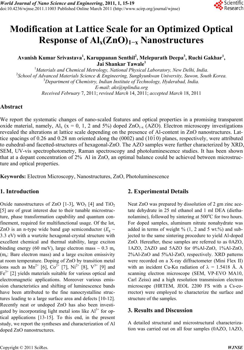 World Journal of Nano Science and Engineering, 2011, 1, 15-19 doi:10.4236/wjnse.2011.11003 Published Online March 2011 (http://www.scirp.org/journal/wjnse) Copyright © 2011 SciRes. WJNSE Modification at Lattice Scale for an Optimized Optical Response of Alx(ZnO)1−x Nanostructures Avanish Kumar Srivastava1, Karuppanan Senthil2, Melepurath Deepa3, Ruchi Gakhar1, Jai Shankar Tawale1 1Materials and Chemical Metrology, National Physical Laboratory, New Delhi , I ndia. 2School of Advanced Materials Science & Engineering, Sungkyunkwan University, Suwon, South Korea. 3Department of Chemistry, Indian Institute of Technology, Hyderabad, India. E-mail: aks@nplindia.org Received February 7, 2011; revised March 14, 2011; accepted March 18, 2011 Abstract We report the systematic changes of nano-scaled features and optical properties in a promising transparent oxide material, namely, Alx (x = 0, 1, 2 and 5%) doped ZnO1-x (AZO). Electron microscopy investigations revealed the alterations at lattice scale depending on the presence of Al-content in ZnO nanostructures. Lat- tice spacings of 0.26 and 0.28 nm oriented along the (0002) and (1010) planes, respectively, were attributed to euhedral-and facetted-structures of hexagonal-ZnO. The AZO samples were further characterized by XRD, SEM, UV-vis spectrophotometry, Raman spectroscopy and photoluminescence studies. It has been shown that at a dopant concentration of 2% Al in ZnO, an optimal balance could be achieved between microstruc- ture and optical properties. Keywords: Electron Microscopy, Nanostructures, ZnO, Photoluminescence 1. Introduction Oxide nanostructures of ZnO [1-3], WO3 [4] and TiO2 [5] are of great interest due to their tunable microstruc- ture, phase transformation capability and quantum con- finement, required for multifunctional usage. Of the lot, ZnO is an n-type wide band gap semiconductor (Eg ~ 3.3 eV) with a wurtzite hexagonal-crystal structure with excellent chemical and thermal stability, large exciton binding energy (60 meV), large electron mass ~ 0.3 me (me: Bare electron mass) and a large exciton emissivity at room temperature. Doping of ZnO by transition metal ions such as Mn2+ [6], Co2+ [7], Ni2+ [8], V3+ [9] and Fe3+ [2] yields materials suitable for various optical and electromagnetic applications. Moreover various emis- sion characteristics and shifting of luminescence bands have been attributed to the fine nanocrystalline struc- tures leading to a large surface area and defects [10-12]. Recently neat or undoped ZnO has also been investi- gated by incorporating light metal ions like Al3+ for op- tical applications [13-15]. To this end, in the present study, we report the syntheses and characterization of Al doped ZnO nanostructures. 2. Experimental Details Neat ZnO was prepared by dissolution of 2 gm zinc ace- tate dehydrate in 25 ml ethanol and 1 ml DEA (dietha- nolamine), followed by sintering at 500oC for two hours. For doped samples, aluminum nitrate nonahydrate was added in terms of weight % (1, 2 and 5 wt.%) and sub- jected to the same sintering procedure to yield Al-doped ZnO. Hereafter, these samples are referred to as 0AZO, 1AZO, 2AZO and 5AZO for 0%Al-ZnO, 1%Al-ZnO, 2%Al-ZnO and 5%Al-ZnO, respectively. XRD patterns were recorded on a X-ray diffractometer (Mini Flex II) with an incident Cu-Kα radiation of = 1.5418 Å. A scanning electron microscope (SEM, VP-EVO MA10, Carl Zeiss) and a high resolution transmission electron microscope (HRTEM, JEOL 2200 FS with a Cs-co- rrector) were employed to characterize the surface and structure of the samples. 3. Results and Discussion A detailed structural and microstructural characteriza- tion was carried out on all four samples (0AZO, 1AZO,  A. K. SRIVASTAVA ET AL. Copyright © 2011 SciRes. WJNSE 16 INTENSITY(arb.units) 10 20 30 40 50 60 70 80 2θ ( de g rees ) 2021 0004 2022 1120 1012 1011 0002 1010 1013 2020 1122 Figure 1. XRD pattern of 0AZO sample showing the presence of important planes of ZnO-hexagonal crystal structure. a b a b c d Figure 2. SEM micrographs of AZO samples with x = 0 (a),1 (b), 2 (c) and 5 (d) showing the fine topographical fea- tures on the surface of these samples. Insets in individual micrographs further reveal the high magnification surface microstructures. 2AZO and 5AZO). It was noted that all the four samples exhibited the characteristic peaks of hexagonal – ZnO (wurtzite type; a = 0.32, c = 0.52 nm, reference: JCPDS file no. 21-1486) in X-ray diffractogram (XRD). As an illustrative example, a XRD pattern of 0AZO sample exhibiting the intense planes (hkil); 1010, 0002, 1011,1012, 1120, 1013, 2020, 1122, 2021, 0004 and 2022 with interplanar spacing (d); 0.28, 0.26, 0.25, 0.19, 0.16, 0.15, 0.14, 0.138, 0.136, 0.130 and 0.124, respectively, are marked on diffraction peaks (Figure 1). Further analyses inferred that, initially, the intensity of the 1010 peak decreases in 1AZO, as compared to 0AZO, but ongoing to 2AZO, the intensity of this peak is higher than that of 0AZO. But for the 5AZO sample, the intensity of this peak falls again. The crystallite size estimated from the Scherrer’s formula was 5.12, 5.12, 6.14 and 4.72 nm for 0, 1, 2 and 5% AZO samples, re- spectively. The surface topography and microstructures of the samples are analyzed by scanning electron microscopy (Figure 2). These samples are consisted of different morphologies depending on the dopant concentration. In an undoped condition, normally a dense fine size parti- cles are seen (Figure 2a). On increasing the magnifica  A. K. SRIVASTAVA ET AL. Copyright © 2011 SciRes. WJNSE 17 Figure 3. HRTEM micrographs of AZO samples with x = 0 (a,b), 1 (c,d), 2 (e,f). (a,b) lattice scale images of nanoparticles as shown in insets of (a) and (b). SADPs as shown in the left hand side insets of (a) and (b) correspond to the respective nanopar- ticles. (c) bright field micrograph and (d) lattice scale image of a nanoparticle (inset of d). Inset in (c) is the corresponding SADP. (e) bright field micrograph, (f) lattice scale image of a nanoparticle shown as an inset in (e). SADP of nanoparticle is also shown as an inset in (e). tion, the particles with the size between 50 to 150 nm are resolved in the micrograph (inset of Figure 2a). On addition of 1%Al as dopant, there is a change in mor- phology of the nanoparticles having worm-like appear- ance with a coarse-structure (Figure 2b) with a very smooth surface (inset of Figure 2b). On further increase in dopant concentration microstructural transformation takes place from worm-like to random particles with carrying more like individual identity (Figure 2c). At high magnification, the surface of these individual parti- cles have developed some cellular microstructure which was seen on every individual nanoparticle (inset of Fig- ure 2c). At highest dopant concentration (5% Al) the microstructure is refined (Figure 2d) compared to pre- vious one (2% Al, Figure 2c) and the surface micro- structure was also grown (inset of Figure 2d). It is also seen that on increasing the dopant concentration, the agglomeration among nanoparticles increases and it is significant at highest doping (Figure 2d). It is probably due to the fact at high doping, the excess Al, precipitates and goes into the interparticle boundaries and tries to act as binder between the particles. Sometimes the precipi- tation is so obvious that the excess Al starts forming its own commonly known dendritic structure (inset as left top corner of Figure 2d). High resolution transmission electron microscopy was employed to investigate the neat and Al-doped ZnO samples even at atomic scale and in reciprocal space. In the 0AZO sample, well facetted grains with euhedral shapes (diameter ~ 80 nm and length ~ 180 nm) having conical tips were observed (inset of Figure 3a). The corresponding lattice scale image (Figure 3a) shows a set of planes with an interplanar spacing of 0.26 nm ori- ented along the 0002 direction. The nanoparticles have a hexagonal structure with each facet of about 40 nm (in- set of Figure 3b). The corresponding lattice scale image (Figure 3b) shows a set of planes with an interplanar spacing of 0.28 nm oriented along the 1010 reflection. Selected area electron diffraction patterns (SADPs) re- corded from a euhedral grain (inset of Figure 3a) ori- ented along the [1216] zone axis (inset of Figure 3a) and from a hexagonal crystallite (inset in Figure 3b) oriented along the [0001] zone axis (inset of Figure 3b). Since the lattice image in Figure 3b has been recorded along the [0001] zone axis which is also the c-axis of hexagonal ZnO, six planes of oriented along the {1010} direction are clearly seen. For the 1AZO sample, nanoparticles tend to aggregate and the diameter of these particles varies from 15 to 30 nm (Figure 3c). A high resolution image recorded from one such nanoparticle (inset of Figure 3d) shows that these particles have lat- tice scale defects as shown by the encircled region in Figure 3d. On either side of the encircled region, the structure is regular with an interplanar spacing of 0.26 nm that corresponds to the 0002 plane of hexagonal ZnO. The corresponding SADP, recorded along the [0110] c a e f b d  A. K. SRIVASTAVA ET AL. Copyright © 2011 SciRes. WJNSE 18 Figure 4. Lattice scale image of a nanoparticle of about 90 nm, shown as inset. The inset on the right hand side shows a cluster of nanoparticles. a b Figure 5. (a) Raman and (b) photoluminescence spectra of AZO samples. 1 = 0AZO, 2 = 1AZO, 3 = 2AZO and 4 = 5AZO. zone axis is displayed as an inset of Figure 3c. For the 2AZO sample fine nanoparticles (of about 20 nm diame- ter) embedded in larger sized particles were seen (Fig- ure 3e). A defect free image recorded along the c-axis of the hexagonal crystal structure (Figure 3f) from a parti- cle of about 70 nm size (inset of Figure 3e). For the 5AZO sample, dislocations and other prominent defects at lattice scale were observed and these have been en- circled by dotted lines (Figure 4). These defects were seen in high resolution image of a nanoparticle of about 90 nm diameter (inset of Figure 4), isolated from a clus- ter of nanoparticles (inset of Figure 4). In general the XRD analyses also corroborate the electron microscopy investigations. Raman spectra recorded at a wavelength of 532 nm for all AZO samples, shows that the overall features of the spectra remain the same except for the two peaks observed at 328 and 432 cm-1 (Figure 5a). These Raman active modes are ascribed to the multi-phonon process (326 cm-1) and the E22 high phonon mode (436 cm-1) [13-15]. It is evident from Raman spectra, that the varia- tion in the intensity of the peaks is due to the incorpora- tion of Al3+. Initially for 1AZO sample, the intensity of the Raman bands decreases as compared to 0AZO but for 2AZO, the intensity increases in comparison to 0AZO (Figure 5a). For 5AZO, the intensity of Raman peaks again decreases. However, the 1AZO sample was characterized by peaks with least intensity (Figure 5a). This behavior may be associated with the change the degree of crystallinity of undoped ZnO induced by dop- ing with Al3+. From XRD and electron microscopy ex- periments, the size of the nanocrystallites varies in a same manner as the intensity profile of Raman active bands does. The wurtzite-hexagonal structure of ZnO is non-centrosymmetric and the Zn atom (63.59 amu) is about four times heavier than that of oxygen atom (15.999 amu), and therefore the structure is polar. On introducing Al3+ in the ZnO lattice, the non-polar inter- action becomes strong. Initially the structure tries to stabilize by filling the vacancies and defect centers at low dopant levels (1AZO). However in 2AZO, the non- polar phonon mode (E22 high mode at 436 cm-1) is stronger with respect to that observed for 0AZO. The quality of nanostructured-ZnO improves with the addi- tion of dopant like Al3+, with 2AZO being the sample with high crystallinity and a uniform almost defect free structure. The transmittance spectra recorded within the 300 ≤ ≤ 700 nm wavelength range revealed that the transmit- tance was almost same (~ 50%) for 0AZO and 2AZO samples and this value was reduced for the other two samples, 1AZO and 5AZO to about 35% in the same wavelength range. Photoluminescence spectra of all the four samples of AZO recoded at an excitation wave- length of 320 nm are shown in Figure 5b. Four bands [2] were seen in all spectra and these have assigned as follows: 1) 377 nm (3.29 eV): excitonic emission due to the recombination of excited electron with a hole to form a pair of exciton in the valence band, 2) 425 nm (2.91 eV): transition between conduction band (CB) and 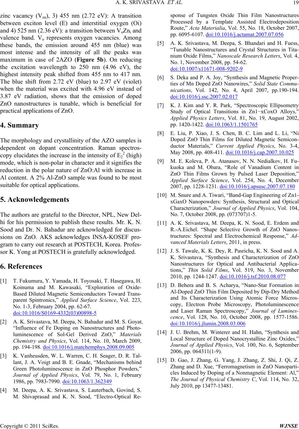 A. K. SRIVASTAVA ET AL. Copyright © 2011 SciRes. WJNSE 19 zinc vacancy (Vzn), 3) 455 nm (2.72 eV): A transition between exciton level (E) and interstitial oxygen (Oi) and 4) 525 nm (2.36 eV): a transition between VoZni and valence band. Vo represents oxygen vacancies. Among these bands, the emission around 455 nm (blue) was most intense and the intensity of all the peaks was maximum in case of 2AZO (Figure 5b). On reducing the excitation wavelength to 250 nm (4.96 eV), the highest intensity peak shifted from 455 nm to 417 nm. The blue shift from 2.72 eV (blue) to 2.97 eV (violet) when the material was excited with 4.96 eV instead of 3.87 eV radiation, shows that the emission of doped ZnO nanostructures is tunable, which is beneficial for practical applications of ZnO. 4. Summary The morphology and crystallinity of the AZO samples is dependent on dopant concentration. Raman spectros- copy elucidates the increase in the intensity of E22 (high) mode, which is non-polar in character and it signifies the reduction in the polar nature of ZnO:Al with increase in Al content. A 2% Al-ZnO sample was found to be most suitable for optical applications. 5. Acknowledgements The authors are grateful to the Director, NPL, New Del- hi for his permission to publish these results. Mr. K. N. Sood and Dr. N. Bahadur are acknowledged for discus- sions on ZnO. AKS acknowledges INSA-KOSEF pro- gram to carry out research at POSTECH, Korea. Profes- sor K. Yong at POSTECH is gratefully acknowledged. 6. References [1] T. Fukumura, Y. Yamada, H. Toyosaki, T. Hasegawa, H. Koinuma and M. Kawasaki, “Exploration of Oxide- Based Diluted Magnetic Semiconductors Toward Trans- parent Spintronics,” Applied Surface Science, Vol. 223, No. 1-3, February 2004, pp. 62-67. doi:10.1016/S0169-4332(03)00898-5 [2] A. K. Srivastava, M. Deepa, N. Bahadur and M. S. Goyat, “Influence of Fe Doping on Nanostructures and Photo- luminescence of Sol-Gel Derived ZnO,” Materials Chemistry and Physics, Vol. 114, No. 10, March 2009, pp. 194-198. doi:10.1016/j.matchemphys.2008.09.005 [3] K. Vanheusden, W. L. Warren, C. H. Seager, D. R. Tal- lant, J. A. Voigt and B. E. Gnade, “Mechanisms behind Green Photoluminescence in ZnO Phosphor Powders,” Journal of Applied Physics, Vol. 79, No. 1, February 1986, pp. 7983-7990. doi:10.1063/1.362349 [4] M. Deepa, A. K. Srivastava, S. Lauterbach, Govind, S. M. Shivaprasad and K. N. Sood, “Electro-Optical Re- sponse of Tungsten Oxide Thin Film Nanostructures Processed by a Template Assisted Electrodeposition Route,” Acta Materialia, Vol. 55, No. 18, October 2007, pp. 6095-6107. doi:10.1016/j.actamat.2007.07.056 [5] A. K. Srivastava, M. Deepa, S. Bhandari and H. Fuess, “Tunable Nanostructures and Crystal Structures in Tita- nium Oxide Films,” Nanoscale Research Letters, Vol. 4, No. 1, November 2008, pp. 54-62. doi:10.1007/s11671-008-9202-9 [6] S. Deka and P. A. Joy, “Synthesis and Magnetic Proper- ties of Mn Doped ZnO Nanowires,” Solid State Commu- nications, Vol. 142, No. 4, April 2007, pp.190-194. doi:10.1016/j.ssc.2007.02.017 [7] K. J. Kim and Y. R. Park, “Spectroscopic Ellipsometry Study of Optical Transitions in Zn1−xCoxO Alloys,” Applied Physics Letters, Vol. 81, No. 19, August 2002, pp. 1420-1422. doi:10.1063/1.1501765 [8] E. Liu, P. Xiao, J. S. Chen, B. C. Lim and L. Li, “Ni Doped ZnO Thin Films for Diluted Magnetic Semicon- ductor Materials,” Current Applied Physics, No. 3-4, May 2008, pp. 408-411. doi:10.1016/j.cap.2007.10.025 [9] M. E. Koleva, P. A. Atanasov, N. N. Nedialkov, H. Fu- kuoka and M. Obara, “Role of Vanadium Content in ZnO Thin Films Grown by Pulsed Laser Deposition,” Applied Surface Science, Vol. 254, No. 4, December 2007, pp. 1228-1231. doi:10.1016/j.apsusc.2007.07.180 [10] M. Snure and A. Tiwari, “Band-Gap Engineering of Zn1- xGaxO Nanopowders: Synthesis, Structural and Optical Characterization,” Journal of Applied Physics, Vol. 104, No. 7, October 2008, pp. (073707)1-5. [11] A. K. Srivastava, M. Deepa, K. N. Sood, E. Erdem and R.-A.Eichel. “Shape Selective Growth of ZnO Nanos- tructures: Spectral and Electrochemical Response,” Ad- vanced Materials Letters, 2011, in press. [12] J. S. Tawale, K. K. Dey, R. Pasricha, K. N. Sood and A. K. Srivastava, “Synthesis and Characterization of ZnO Nanostructures for Optical and Antibacterial Applica- tions,” Thin Solid Films, Vol. 519, No. 3, November 2010, pp. 1244-1247. doi:10.1016/j.tsf.2010.08.077 [13] D. Behera and B. S. Acharya, “Nano-Star Formation in Al-Doped ZnO Thin Film Deposited by Dip-Dry Method and Its Characterization Using Atomic Force Micros- copy, Electron Probe Microscopy, Photoluminescence and Laser Raman Spectroscopy,” Journal of Lumines- cence, Vol. 128, No. 10, October 2008, pp. 1577-1586. doi:10.1016/j.jlumin.2008.03.006 [14] J. U. Brehm, M. Winterer and H. Hahn, “Synthesis and Local Structure of Doped Nanocrystalline Zinc Oxides,” Journal of Applied Physics, Vol. 100, No. 6, September 2006, pp. 064311(1-9). [15] D. Gao, J. Zhang, G. Yang, J. Zhang, Z. Shi, J. Qi, Z. Zhang and D. Xue, “Ferromagnetism in ZnO Nanoparti- cles Induced by Doping of a Nonmagnetic Element: Al,” The Journal of Physical Chemistry C, Vol. 114, No. 32, July 2010, pp 13477-13481. |