Circuits and Systems
Vol.07 No.09(2016), Article ID:69136,15 pages
10.4236/cs.2016.79223
Design and Implementation of an Efficient Reversible Comparator Using TR Gate
Subramanian Saravanan1*, Ila Vennila1, Sudha Mohanram2
1Department of EEE, P. S. G. College of Technology, Coimbatore, India
2Sri Eshwar College of Engineering, Kondampatty, India

Copyright © 2016 by authors and Scientific Research Publishing Inc.
This work is licensed under the Creative Commons Attribution International License (CC BY).
http://creativecommons.org/licenses/by/4.0/


Received 5 April 2016; accepted 20 April 2016; published 27 July 2016
ABSTRACT
Reversible logic is a new emerging technology with many promising applications in optical information processing, low power (Complementary Metal Oxide Semiconductor) CMOS design, (De Oxy RiboNucleic Acid) DNA computing, etc. In industrial automation, comparators play an important role in segregating faulty patterns from good ones. In previous works, these comparators have been implemented with more number of reversible gates and computational complexity. All these comparators use propagation technique to compare the data. This will reduce the efficiency of the comparators. To overcome the problem, this paper proposes an efficient comparator using (Thapliyal Ranganathan) TR gate utilizing full subtraction and half subtraction algorithm which will improve the computation efficiency. The comparator design using half subtraction algorithm shows an improvement in terms of quantum cost. The comparator design using full subtraction algorithm shows effectiveness in reducing number of reversible gates required and garbage output.
Keywords:
Reversible Logic Gates, Reversible Logic Circuits, (Very Large Scale Integration) VLSI Design

1. Introduction
Moore’s law states that number of transistors in a chip doubles every two years but chip size decreases. This cannot be reduced greatly which will lead to more power consumption. This paves the path to new technologies “Reversible logic” and “Quantum dot Cellular Automata (QCA)”. As stated by Launder during logical computation, a bit of information is lost. It dissipates 2ln (KT) energy, where K is Boltzman constant and T is temperature. Present day computers are formed of digital logic circuits where one bit of information is lost for every computation. This is called irreversible logic [1] . To overcome this problem Bennett proposed number of inputs and outputs makes equal which will dissipate less power as bits are preserved at the output [2] . This is called Reversible logic. A quantum computer uses principle of superposition and entanglement for qubit computation (quantum bit―the basic unit of information for quantum computers). Reversible logic plays an important role in converting classical computation to quantum computation. The basic properties of Reversible logic are:
Equal number of inputs and outputs
Unique nature of outputs one to one mapping.
The Input and Output mapping is shown in Figure 1.
Minimum garbage output
No feedback
No fan out
Minimum number of reversible gates to be used
Minimum number of constant inputs.
The number of 1 × 1 or 2 × 2 reversible gates needed to design a reversible logic circuit is called quantum cost.
The number of reversible gates including 3 × 3 and 4 × 4 reversible gates needed to design system is the number of reversible gates required.
The unused output in a reversible circuit is called garbage output.
Total logic calculation is the number of XOR, AND, NOT logic function used in the reversible circuit. α indicates number of XOR logic in the circuit; β indicates number of AND logic in the circuit and γ indicates number of NOT logic in the circuit.
Reversible gates are classified as 2 × 2 gates, 3 × 3 gates and 4 × 4 gates. Example for 2 × 2 gates is Feynman gate, and for 3 × 3 gates are Taffoli gate and Peres gate. The Classification of Reversible Logic Gates is given in Figure 2 [25] .

Figure 1. Input and output mapping.

Figure 2. Classification of reversible logic gates.
The basic reversible gates are shown in Figure 3 [3] .
1.1. Reversible Tr Gate
Thapliyal proposed a three input reversible gate called TR gate [3] . A, B and C are inputs and P, Q and R are corresponding outputs. The gate has unique one to one mapping.
The Reversible TR gate is given in Figure 4. The input and output functions are given by equations (1) and (2) respectively.
 (1)
(1)
![]() (2)
(2)
Research in reversible logic is getting importance today. Thapliyal and Srinivasan proposed a new reversible (Thapliyal Srinivasan Gate) TSG gate [4] and discuss about reversible carry look ahead adder and other adder architecture which forms a part of (Arithmetic and Logic Unit) ALU. The quantum cost of TSG gate is quiet high when compared to (Haghparast Navi Gate) HNG gate. Haghparast proposes two new 4 × 4 bit reversible multiplier designs with less hardware complexity, less garbage bits, less quantum cost, and less constant inputs [5] and the architecture uses Peres gate for partial product generation. But the total logical calculation is more due to extra logics in Peres gate. Research is going on in deriving more applications out of it. Research is moving towards deriving a new application from reversible gates. Ancient Indians followed some sutras or formulae
![]()
Figure 3. Basic reversible gates.
![]()
Figure 4. Reversible TR gate.
for mathematical computation. These basic mathematical calculations form the base for modern VLSI architecture. Thapliyal discussed about performance of Vedic multipliers on (Field Programmable Gate Array) FPGA [6] and discusses the irreversible architecture based on delay. These architectures when implemented in VLSI will reduce power consumption. Ehsan Pour Ali Akbar, et al. proposed reversible signed Wallace tree multiplier in [7] . Synthesis of reversible circuits is discussed in [8] - [13] . It discusses about Binary Decision Diagram synthesis methods, exact synthesis approach and transformation based synthesis. Testing of reversible circuits is discussed in [14] .
Research in reversible logic is getting importance today. Nagamani et al. presented reversible 1 bit comparators [15] . The comparators were designed using BJN gate, Peres gate and Feynman gate. Lihui et al. proposed reversible 4 bit comparator using NLG gate [16] . NLG gate is a 2 × 2 reversible gate. The gate works on the principle that when both inputs are same second output is one. This is similar to EXNOR logic. It is considered as complement of Feynman gate. Haghparast et al. proposed a 4 bit comparator using subtraction logic using HNG gate adopting carry propagation technique [17] . It requires 4 HNG gates, 4 Peres gates and 2 Feynman gates for 4 bit comparator design. Molecular design of half subtractor using Tetraphenylporphyrin was discussed in [18] . Kaur et al. discussed about Reversible design of full adder/full subtractor in [19] . The design uses parity preserving gate used in fault tolerant systems. Normally Fredkin gate is used as parity preserving logic. The uniqueness of the system is that number of “1”s in input is equal to number of “1” s in output. Haghparast proposed a new reversible (Binary Coded decimal) BCD subtractor using genetic algorithm in [20] . Haghparast proposed fault tolerant reversible BCD adder in [21] . The design uses fault tolerant NFT reversible gates and F2G gates. It provides an optimized design. Haghparast proposed reversible BCD adder/subtractor in [22] . The reversible BCD adder/subtractor units were designed using genetic algorithm for optimization approaches.
This paper designs a reversible comparator using TR gate proposed by Thapliyalusing full subtraction and half subtraction algorithm and analyzes the performance of the comparators in terms of quantum cost, number of gates and garbage output. The rest of the paper discusses proposed comparator design in Chapter 2, results and discussion in Chapter 3 and finally conclusion.
2. Proposed Comparator
In present day industrial automation, comparators play a major role. Digital comparator are used in computer processors, and moreover it can be used in some industrial automation devices that contrast visual images with digital images, as in the case of mechanical engineering industry that relies on computer-aided drafting (CAD) programs to check good products from faulty ones. They also can be employed to convert analog signals into digital patterns. A digital comparator also can be used along with a number of other devices to act as a monitor in an industrial setting to monitor accurate state of a machine. In view of importance of comparator in many industrial applications, this paper proposes reversible comparator design using TR gate proposed by Thapliyal (it is used as full subtractor). The comparator is designed with full subtraction algorithm and half subtraction algorithm. The proposed design is compared with previous works in terms of Quantum Cost, number of reversible gates, number of garbage outputs.
2.1. Comparator System Design
The comparator system consists of data segregator, comparator using the above algorithms and equvalence checker. The comparator system is shown in Figure 5. The data segregator as already described in algorithm it segregates the incoming data into Least Significant Bits (LSB) and Most Significant Bits (MSB). First the segregated MSB data is passed through the comparator which uses half subtraction or full subtraction algorithm. The carry and difference obtained is compared with to get data is greater or smaller.
2.2. Reversible Comparator Using Full Subtraction Method
Reversible comparator is designed based on the subtraction algorithm. The paper uses full subtraction algorithm to compare 4 bit data. Carry is propagated between the bits. The same algorithm is used to design reversibe comparator based on TR gate subtractor. The design using TR gate requires 8 TR gates. To implement a subtractor module, 2 TR gates are needed. For 4 bit subtraction 8 TR gates are required. When end carry arises, A < B. When end carry is “0”, A > B. When all the difference bits and end carry bits are zero, then A = B. Each pair of TR gate acts as full subtractor. The architecture diagram for reversible comparator using full subtraction algorithm is shown in Figure 6.
In the comparator architecture shown below Q0-Q3 represents difference bits, R0-R3 represents borrow bits. For bits if borrow occurs Cout is “1”. A < B. If borrow does not occur and if the difference is zero, then A = B. If borrow does not occurs but if the difference is not zero then A > B. It involves carry propagation, so it is expected that computation delay will be little bit higher.
2. 3. Reversible Comparator Using Half Subtraction Method
Reversible comparator is designed based on the half subtraction algorithm. This paper uses half subtraction algorithm to compare 4 bits of data. Carry is not propagated between the bits. Instead the carry generated in each bit is used to judge the comparison. The 4 bit data is divided into two sets of data LSB and MSB. The algorithm is explained below. The algorithm is used to design reversibe comparator based on TR gate subtractor. The design using TR gate requires 4 TR gates. To implement a half subtractor module, 1 TR gates is needed. For 4 bit subtraction 4 TR gates are required. The architecture diagram for reversible comparator using half subtr- action algorithm is shown in Figure 7.
![]()
Figure 5. Comparator system.
![]()
Figure 6. Architecture diagram for reversible comparator using full subtraction algorithm.
![]()
Figure 7. Architecture diagram for reversible comparator using half subtraction algorithm.
In the comparator architecture shown below D0-D3 represents difference bits, B0-B3 represents borrow bits. The data is verified from MSB to LSB. For MSB bits if borrow occurs. A < B. If borrow does not occur and if the difference is zero, then A = B. If borrow does not occurs but if the difference is not zero then A > B. To check the last two conditions equivalence checker is used. Since data verififcation starts from MSB to LSB, it is expected that computation delay will be less.
ALGORITHM
Ø Segregate the 4 bit data and perform half subtraction on each of the minuend and subtrahend seperately.
Ø Check from MSB, if carry occurs in the MSB, then subtrahend is greater.
Ø If carry does not occur in MSB and difference is also “1”, then minuend is greater.
Ø Else if carry does not occur in MSB and difference is also “0”, then check in next bit position if carry occurs then subtrahend is greater and repeat this for next set of bits.
Ø If carry does not occur and difference is also ‘0’, then the two bits are equal.
Ø If carry does not occur and difference results then minuend is greater.
2.4. Equivalence Checker
The equivalence checker consists of feynman gates. The gate uses EXOR logic which is used to compare the data obtained from comparator with predefined pattern. The equivalence checker is given in Figure 8. The equivalence architecture shown below is scalable for ant number of bits. In the equivalence architecture borrow and difference bits obtained from comparator stage (TR half subtraction) is passed and verified. For eg. If D3 is zero and is passed through equivalence checker, the checker output is zero. Otherwise if D3 is not zero and is passed through equivalence checker,the checker output is not zero. In this case borrow B3 has to be checked, if in the equivalence checker output is one, then A < B, otherwise A > B.
3. Results and Discussions
The proposed method is verified for functional verification in Xilinx 9.2 using verilog simulator. The results for Comparator using the full subtraction algorithm is shown in Figure 9. Results for Comparator using half subtraction algorithm is shown in Figure 10.
In Figure 9 a1, b1 and c1 are inputs, z1 is the difference output and r21 is the carry output. If a1 = 4, b1 = 2, c1 = 0, then the difference z1 is 2, carry r21 is “0”. This indicates a1 > b1. If a1 = 2, b1 = 4, c1 = 0, then the difference z1 is E, carry r21 is “1”. This indicates a1 < b1. If a1 = 4, b1 = 4, c1 = 0, then the difference z1 is “0”, carry r21 is “0”. This indicates a1 = b1.
In Figure 10, case 1 consider the data “21” & “20”. The data are segregated into MSB and LSB bits as discussed below.When the data are subtracted from MSB bits, MSB bits are equal as difference and carry is “0”. So next LSB bits are considered for computation. The difference is “1” and carry is “0” which indicates miuend is greater.
![]()
Figure 8. Equivalence checker.
![]() 1. A > B
1. A > B![]() 2. A < B
2. A < B![]() 3. A = B
3. A = B
Figure 9. Results for Comparator using the full subtraction algorithm.
a1 and b1 corresponds to MSB bits. c1 and d1 corresponds to LSB bits are inputs, q2 and q3 corresponds to difference bits and r and r1 corresponds to carry bits. Here a1 and c1 are minuend, b1 and d1 are subtrachend. If a1 = 2, b1 = 2, c1 = 1 and d1 = 0, then the difference occurs in q3 and carry does not occur.This indicates miuend is greater.
Case 2 consider the data “32” & “22”. The data are segregated into MSB and LSB bits as discussed below.When the data are subtracted from MSB bits, MSB bits are not equal difference occurs and carry does not occur. The difference is “1” and borrow is “0” which indicates miuend is greater. If a1 = 3, b1 =2, c1 =2 and d1 = 2, then the difference occurs in q2 and carry does not occur. This indicates miuend is greater.
Case 3 consider the data “21’ & “22”. The data are segregated into MSB and LSB bits as discussed below.When the data are subtracted from MSB bits, MSB bits are equal difference does not occurs and carry does not occur.So next LSB bits are considered, “1” and “2” when subtracted difference is”1’ and carry is “1”. If a1 = 2, b1 = 2, c1 = 1 and d1 = 2, then the difference occurs in q3 and carry also occurs. This indicates subtrahend is greater.
Case iv consider the data “22” & “32”. The data are segregated into MSB and LSB bits as discussed below.When the data are subtracted from MSB bits, MSB bits are not equal difference occurs and carry also occur. The data “2” and “3” when subtracted difference is “1” and carry is “1”. If a1 = 2, b1 = 3, c1 = 2 and d1 = 2, then the difference occurs in q2 and carry also occurs. This indicates subtrahend is greater.
TheComparitive analysis of reversible comparators is given in Table 1. On comparison the number of reversible gates required in the comparison using subtraction algorithm is less and also garbage output is also less. Quantum cost of TR gate is 6 [3] . So for 4 bit comparator design total quantum cost is 48. It is little bit higher than the existing one. The proposed comparator using half subtraction algorithm has quantum cost of 24. The comparator using half subtraction algorithm requires less quantum cost, number of reversible gates and garbage output.
In the existing technique [17] HNG gate is used, peres gate and feynman gate are used. It is three level network. The number of garbage output is two for HNG gate and for peres gate also garbage output is two. In [23] tree based approach is used. This involves signal propagation incurs compuational delay.
 Case 1
 Case 2
 Case 3
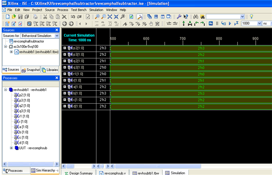 Case 4
Figure 10. Results for Comparator using half subtraction algorithm.
In the existing technique [24] four ZRQC1 gates, 6 Peres gates and 3 Feynman gates are used. It is multi level network and moreover the data is propagated. This obviously pass on the delay. Computational delay will be more. In [15] by using BJN reversible gate and TR gate, for one bit comparision three reversible gates are needed. This increases cost overhead. When the nmber of gates increases computational delay also increases. Similarly for one bit comparision, using Peres gate and BJN gate, 3 reversible gates are needed. By using Taffoli and BJN gate 4 reversible gates are needed to design one bit comparator. By using Fredkin and BJN gate for one bit comparision it requires 5 reversible gates.
In the proposed method, TR gate and Feynman gate are used in half subtraction mode which generates less garbage output and less quantum cost. The data is checked from MSB to LSB. If in the MSB, carry generated then there is no need for comparison of successive bits. This reduces delay in comparison for higher value of MSB.
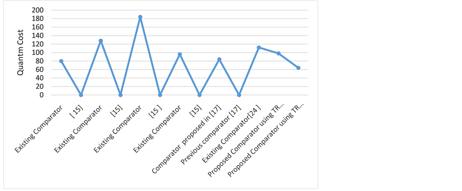
The Comparitive analysis of reversible comparators for 8 bit comparator is shown in Table 2. From the table it is inferred that number of gates and garbage output doubles but compartor using half subtraction algorithm yields good results. The comparison of various comparators based on quantum cost, garbage output and number of gates are shown in Figures 11(a)-(c) respectively.
From Figure 11(a) it is found that comparator design using BJN gate and Fredkin gate offers high quantum cost. The proposed comparator using half subtraction algorithm offers less quantum cost. From Figure 11(b) it is found that comparator design using NLG gate offers higher number of reversible gates. The proposed comparator using full subtraction algorithm offers less number of reversible gates. From Figure 11(c) it is found that comparator design using BJN gate and Fredkin gate offers high garbage output. The proposed comparator using full subtraction algorithm offers less garbage output.
4. Conclusion
In this paper, a reversible comparator using TR gate based on full subtraction algorithm and half subtraction

Table 1. Comparative analysis of reversible comparators.
Table 2. Comparative analysis of reversible comparators for 8 bit comparators.
 (a)
(a) (b)
(b) (c)
(c)
Figure 11. (a) Comparison of various comparators based on quantum cost. (b) Comparison of various comparators based on garbage output. (c) Comparison of various comparators based on number of gates.
algorithm was presented and analyzed with existing comparators. It is found that comparator designed half subtraction algorithm using TR gate shows effectiveness in terms of quantum cost but at the expense of number of reversible gates and garbage output. Reversible comparator using full subtraction algorithm proposed is performing better in terms of number of reversible gates and garbage output since equivalence checker circuit is not needed. The same algorithm may be implemented with Delay elements in between by principle of retiming to reduce critical path delay. The future scope of the work is to realize these reversible logic gates in DNA molecules and implement these arithmetic systems so as to reduce power consumption.
Cite this paper
Subramanian Saravanan,Ila Vennila,Sudha Mohanram, (2016) Design and Implementation of an Efficient Reversible Comparator Using TR Gate. Circuits and Systems,07,2578-2592. doi: 10.4236/cs.2016.79223
References
- 1. Landauer, R. (1961) Irreversibility and Heat Generation in the Computing Process. IBM Journal of Research and Development, 5, 183-191.
http://dx.doi.org/10.1147/rd.53.0183 - 2. Bennett, C. (1973) Logical Reversibility of Computation. IBM Journal of Research and Development, 17, 525-532.
http://dx.doi.org/10.1147/rd.176.0525 - 3. Thapliyal, H. and Ranganathan, N. (2011) A New Design of the Reversible Subtractor Circuit. Proceedings of IEEE International Conference on Nanotechnology, Portland, 15-18 August 2011, 1430-1435.
- 4. Thapliyal, H. and Srinivas, M.B. (2005) Novel Reversible “TSG” Gate and Its Application for Designing Reversible Carry Look Ahead Adder and Other Adder Architectures. Springer-Verlag Lecture Notes in Computer Science, Proceedings of the 10th Asia-Pacific Computer Systems Architecture Conference—ACSAC, 3740, 775-786.
- 5. Haghparast, M., Jassbi, S.J., Navi, K. and Hashemipour, O. (2008) Design of a Novel Reversible Multiplier Circuit Using HNG Gate in Nanotechnology. World Applied Sciences Journal, 3, 974-978.
- 6. Thapliyal, H. and Srinivas, M.B. (2004) High Speed Efficient N × N Bit Parallel Hierarchical Overlay Multiplier Architecture Based on Ancient Indian Vedic Mathematic. Transactions on Engineering, Computing and Technology, 2, 225-228.
- 7. Akbar, E.P.A., Haghparast, M. and Keivan Navi, B.N. (2011) Novel Design of a Fast Reversible Wallace Sign Multiplier Circuit in Nanotechnology. Microelectronics Journal, 42, 973-981.
http://dx.doi.org/10.1016/j.mejo.2011.05.007 - 8. Wille, R. and Groβe, D. (2007) Fast Exact Toffoli Network Synthesis of Reversible Logic. Proceedings of International Conference on Computer-Aided Design, San Jose, 4-8 November 2007, 60-64.
http://dx.doi.org/10.1109/iccad.2007.4397244 - 9. Wille, R., Le, H.M., Dueck, G.W. and Groβe, D. (2008) Quantified Synthesis of Reversible Logic. Proceedings of Design Automation & Test Europe Conference, Munich, 10-14 March 2008, 1015-1020.
- 10. Shende, V.V., Prasad, A.K., Markov, I.L. and Hayes, J.P. (2002) Synthesis of Reversible Logic Circuits. Proceedings of International Conference on Computer-Aided Design, 10-14 November 2002, 353-360.
http://dx.doi.org/10.1109/iccad.2002.1167558 - 11. Hung, W.N.N., Song, X., Yang, G., Yang, J. and Perkowski, M. (2004) Quantum Logic Synthesis by Symbolic Reachability Analysis. Proceedings of Design Automation Conference, San Diego, 7-11 July 2004, 838-841.
- 12. Viamontes, G.F., Markov, I.L. and Hayes, J.P. (2007) Checking Equivalence of Quantum Circuits and States. Proceedings of International Conference on CAD, San Jose, 4-7 November 2007, 69-74.
http://dx.doi.org/10.1109/iccad.2007.4397246 - 13. Wang, S.A., Lu, C.Y., Tsai, I.M. and Kuo. S.Y. (2008) An XQDD-Based Verification Method for Quantum Circuits. IEICE Transactions, 91, 584-594.
- 14. Wille, R., Groβe, D., Miller, D.M. and Drechsler, R. (2009) Equivalence Checking of Reversible Circuits. International Symposium on Multi-Valued Logic, Naha, 21-23 May 2009, 324-330.
http://dx.doi.org/10.1109/ismvl.2009.19 - 15. Nagamani, A.N., Jayashree, H.V. and Bhagyalakshmi, H.R. (2011) Novel Low Power Comparator Design Using Reversible Logic Gates. Indian Journal of Computer Science and Engineering, 2, 566-574.
- 16. Ni, L.H., Guan, Z.J., Dai, X.Y. and Li, W.J. (2010) Using New Designed NLG Gate for the Realization of Four-Bit Reversible Numerical Comparator. Proceedings of International Conference on Educational and Network Technology, Qinhuangdao, 25-27 June 2010, 254-258.
- 17. Haghparast, M., Rezazadeh, L. and Seivani, V. (2011) Design and Optimization of Nanometric Reversible 4 Bit Numerical Comparator. Middle-East Journal of Scientific Research, 7, 581-584.
- 18. Langford, S.J. and Yann, T. (2003) Molecular Logic: A Half-Subtractor Based on Tetraphenylporphyrin. Journal of the American Chemical Society, 125, 1198-1199.
- 19. Kaur, P. and Dhaliwal, B.S. (2012) Design of Fault Tolerant Full Adder/ Subtarctor Using Reversible Gates. Proceedings of International Conference on Computer Communication and Informatics (ICCCI), Coimbatore, 10-12 January 2012, 1-5.
- 20. Mohammadi, M., Haghparast, M., Eshghi, M. and Navi, K. (2009) Minimization and Optimization of Reversible BCD-Full Adder/Subtractor Using Genetic Algorithm and Don’t Care Concept. International Journal of Quantum Information, 7, 969-989.
http://dx.doi.org/10.1142/S0219749909005523 - 21. Haghparast, M. (2011) Design and Implementation of Nanometric Fault Tolerant Reversible BCD Adder. Australian Journal of Basic and Applied Sciences, 5, 896-901.
- 22. Mohammadi, M., Eshghi, M., Haghparast, M. and Bahrololoom, A. (2008) Design and Optimization of Reversible BCD Adder/Subtractor Circuit for Quantum and Nanotechnology Based Systems. World Applied Sciences Journal, 4, 787-792.
- 23. Thapliyal, H., Ranganathan, N. and Ferreira, R. (2010) Design of a Comparator Tree Based on Reversible Logic. IEEE International Conference on Nanotechnology, Seoul, August 2010, 1113-1116.
- 24. Zhou, R.-G., Zhang, M.-Q., Wu, Q. and Li, Y.-C. (2013) Optimization Approaches for Designing a Novel 4-Bit Reversible Comparator. International Journal of Theoretical Physics, 52, 559-575.
- 25. Saravanan, S., Vennila, I. and Mohanram, S. (2016) Design and Implementation of Efficient Reversible Arithmetic and Logic Unit. Circuits and Systems, 7, 630-642.
http://dx.doi.org/10.4236/cs.2016.76054
NOTES
![]()
*Corresponding author.