Paper Menu >>
Journal Menu >>
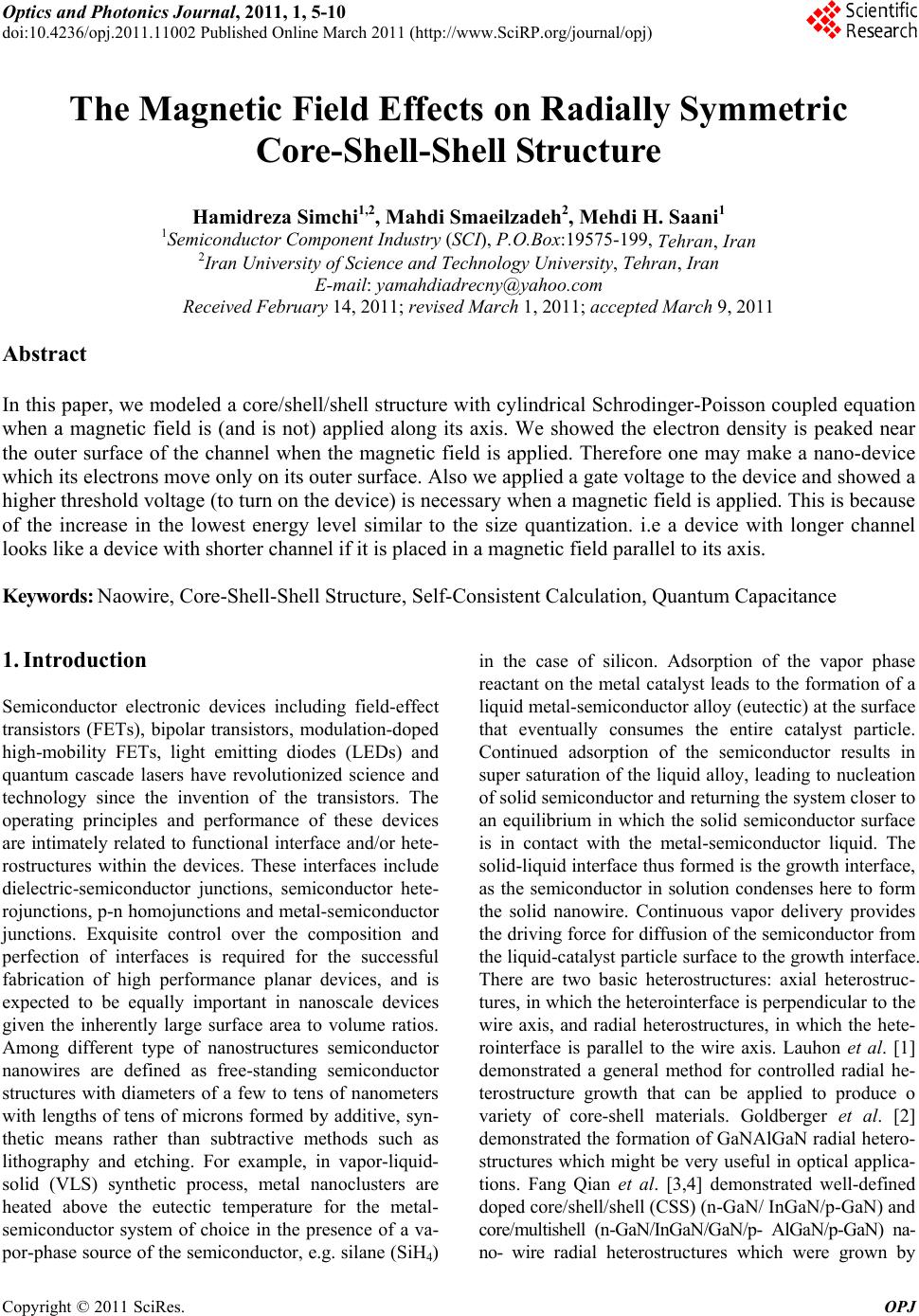 Optics and Photonics Journal, 2011, 1, 5-10 doi:10.4236/opj.2011.11002 Published Online March 2011 (http://www.SciRP.org/journal/opj) Copyright © 2011 SciRes. OPJ The Magnetic Field Effects on Radially Symmetric Core-Shell-Shell Structure Hamidreza Simchi1,2, Mahdi Smaeilzadeh2, Mehdi H. Saani1 1Semiconductor Component Industry (SCI), P.O.Box:19575-199, Teh ran, Iran 2Iran University of Science and Technology University, Tehran, Iran E-mail: yamahdiadrecny@yahoo.com Received February 14, 2011; rev i se d M ar ch 1, 2011; accepted March 9, 2011 Abstract In this paper, we modeled a core/shell/shell structure with cylindrical Schrodinger-Poisson coupled equation when a magnetic field is (and is not) applied along its axis. We showed the electron density is peaked near the outer surface of the channel when the magnetic field is applied. Therefore one may make a nano-device which its electrons move only on its outer surface. Also we applied a gate voltage to the device and showed a higher threshold voltage (to turn on the device) is necessary when a magnetic field is applied. This is because of the increase in the lowest energy level similar to the size quantization. i.e a device with longer channel looks like a device with shorter channel if it is placed in a magnetic field parallel to its axis. Keywords: Naowire, Core-Shell-Shell Structure, Self-Consistent Calculation, Quantum Capacitance 1. Introduction Semiconductor electronic devices including field-effect transistors (FETs), bipolar transistors, modulation-doped high-mobility FETs, light emitting diodes (LEDs) and quantum cascade lasers have revolutionized science and technology since the invention of the transistors. The operating principles and performance of these devices are intimately related to functional interface and/or hete- rostructures within the devices. These interfaces include dielectric-semiconductor junctions, semiconductor hete- rojunctions, p-n homojunctions and metal-semiconductor junctions. Exquisite control over the composition and perfection of interfaces is required for the successful fabrication of high performance planar devices, and is expected to be equally important in nanoscale devices given the inherently large surface area to volume ratios. Among different type of nanostructures semiconductor nanowires are defined as free-standing semiconductor structures with diameters of a few to tens of nanometers with lengths of tens of microns formed by additive, syn- thetic means rather than subtractive methods such as lithography and etching. For example, in vapor-liquid- solid (VLS) synthetic process, metal nanoclusters are heated above the eutectic temperature for the metal- semiconductor system of choice in the presence of a va- por-phase source of the semiconductor, e.g. silane (SiH4) in the case of silicon. Adsorption of the vapor phase reactant on the metal catalyst leads to the formation of a liquid metal-semiconductor alloy (eutectic) at the surface that eventually consumes the entire catalyst particle. Continued adsorption of the semiconductor results in super saturation of the liquid alloy, leading to nucleation of solid semiconductor and returning the system closer to an equilibrium in which the solid semiconductor surface is in contact with the metal-semiconductor liquid. The solid-liquid interface thus formed is the growth interface, as the semiconductor in solution condenses here to form the solid nanowire. Continuous vapor delivery provides the driving force for diffusion of the semiconductor from the liquid-catalyst particle surface to the growth interface. There are two basic heterostructures: axial heterostruc- tures, in which the heterointerface is perpendicular to the wire axis, and radial heterostructures, in which the hete- rointerface is parallel to the wire axis. Lauhon et al. [1] demonstrated a general method for controlled radial he- terostructure growth that can be applied to produce o variety of core-shell materials. Goldberger et al. [2] demonstrated the formation of GaNAlGaN radial hetero- structures which might be very useful in optical applica- tions. Fang Qian et al. [3,4] demonstrated well-defined doped core/shell/shell (CSS) (n-GaN/ InGaN/p-GaN) and core/multishell (n-GaN/InGaN/GaN/p- AlGaN/p-GaN) na- no- wire radial heterostructures which were grown by 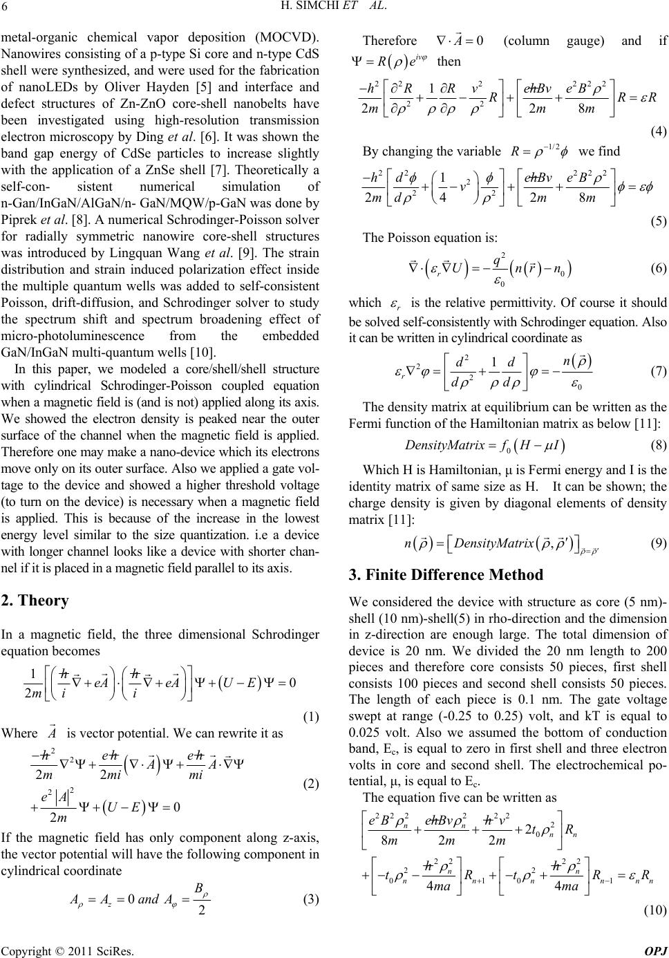 H. SIMCHI ET AL. Copyright © 2011 SciRes. OPJ 6 metal-organic chemical vapor deposition (MOCVD). Nanowires consisting of a p-type Si core and n-type CdS shell were synthesized, and were used for the fabrication of nanoLEDs by Oliver Hayden [5] and interface and defect structures of Zn-ZnO core-shell nanobelts have been investigated using high-resolution transmission electron microscopy by Ding et al. [6]. It was shown the band gap energy of CdSe particles to increase slightly with the application of a ZnSe shell [7]. Theoretically a self-con- sistent numerical simulation of n-Gan/InGaN/AlGaN/n- GaN/MQW/p-GaN was done by Piprek et al. [8]. A numerical Schrodinger-Poisson solver for radially symmetric nanowire core-shell structures was introduced by Lingquan Wang et al. [9]. The strain distribution and strain induced polarization effect inside the multiple quantum wells was added to self-consistent Poisson, drift-diffusion, and Schrodinger solver to study the spectrum shift and spectrum broadening effect of micro-photoluminescence from the embedded GaN/InGaN multi-quantum wells [10]. In this paper, we modeled a core/shell/shell structure with cylindrical Schrodinger-Poisson coupled equation when a magnetic field is (and is not) applied along its axis. We showed the electron density is peaked near the outer surface of the channel when the magnetic field is applied. Therefore one may make a nano-device which its electrons move only on its outer surface. Also we applied a gate vol- tage to the device and showed a higher threshold voltage (to turn on the device) is necessary when a magnetic field is applied. This is because of the increase in the lowest energy level similar to the size quantization. i.e a device with longer channel looks like a device with shorter chan- nel if it is placed in a magnetic field parallel to its axis. 2. Theory In a magnetic field, the three dimensional Schrodinger equation becomes 10 2 hh eAeAU E mi i (1) Where A is vector potential. We can rewrite it as 2 2 2 2 22 0 2 heh eh AA mmi mi eA UE m (2) If the magnetic field has only component along z-axis, the vector potential will have the following component in cylindrical coordinate 02 z B AAand A (3) Therefore 0A (column gauge) and if iv Re then 2 22222 22 1 228 hR RvehBveB RRR mmm (4) By changing the variable 1/2 R we find 2 2222 2 22 1 24 28 hd ehBveB v mmm d (5) The Poisson equation is: 2 0 0 rq Unrn (6) which r is the relative permittivity. Of course it should be solved self-consistently with Schrodinger equation. Also it can be written in cylindrical coordinate as 2 2 2 0 1 r n dd d d (7) The density matrix at equilibrium can be written as the Fermi function of the Hamiltonian matrix as below [11]: 0 DensityMatrixf HI (8) Which H is Hamiltonian, μ is Fermi energy and I is the identity matrix of same size as H. It can be shown; the charge density is given by diagonal elements of density matrix [11]: ,n DensityMatrix (9) 3. Finite Difference Method We considered the device with structure as core (5 nm)- shell (10 nm)-shell(5) in rho-direction and the dimension in z-direction are enough large. The total dimension of device is 20 nm. We divided the 20 nm length to 200 pieces and therefore core consists 50 pieces, first shell consists 100 pieces and second shell consists 50 pieces. The length of each piece is 0.1 nm. The gate voltage swept at range (-0.25 to 0.25) volt, and kT is equal to 0.025 volt. Also we assumed the bottom of conduction band, Ec, is equal to zero in first shell and three electron volts in core and second shell. The electrochemical po- tential, μ, is equal to Ec. The equation five can be written as 2222 22 2 0 22 22 22 0101 2 822 44 nn nn nn nnnnnn eBehBvhv tR mmm hh tRtRR ma ma (10) 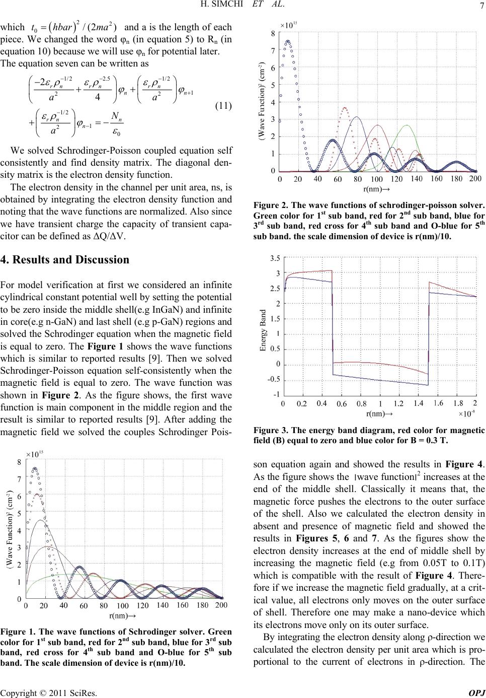 H. SIMCHI ET AL. Copyright © 2011 SciRes. OPJ 7 which 22 0/(2 )thbar ma and a is the length of each piece. We changed the word φn (in equation 5) to Rn (in equation 10) because we will use φn for potential later. The equation seven can be written as 1/22.51/2 1 22 1/2 1 2 0 2 4 rnrnrn nn rn n n aa N a (11) We solved Schrodinger-Poisson coupled equation self consistently and find density matrix. The diagonal den- sity matrix is the electron density function. The electron density in the channel per unit area, ns, is obtained by integrating the electron density function and noting that the wave functions are normalized. Also since we have transient charge the capacity of transient capa- citor can be defined as ΔQ/ΔV. 4. Results and Discussion For model verification at first we considered an infinite cylindrical constant potential well by setting the potential to be zero inside the middle shell(e.g InGaN) and infinite in core(e.g n-GaN) and last shell (e.g p-GaN) regions and solved the Schrodinger equation when the magnetic field is equal to zero. The Figure 1 shows the wave functions which is similar to reported results [9]. Then we solved Schrodinger-Poisson equation self-consistently when the magnetic field is equal to zero. The wave function was shown in Figure 2. As the figure shows, the first wave function is main component in the middle region and the result is similar to reported results [9]. After adding the magnetic field we solved the couples Schrodinger Pois- Figure 1. The wave functions of Schrodinger solver. Green color for 1st sub band, r ed for 2nd sub band, blue for 3rd sub band, red cross for 4th sub band and O-blue for 5th sub band. The scale dimension of device is r(nm)/10. Figure 2. The wave functions of schrodinger-poisson solver. Green col or for 1st sub band, red for 2nd sub band, blue for 3rd sub band, red cross for 4th sub band and O-blue for 5th sub band. the scale dimension of device is r(nm)/10. Figure 3. The energy band diagram, red color for magnetic field (B) equal to zero and blue color for B = 0.3 T. son equation again and showed the results in Figure 4. As the figure shows the ׀wave function׀2 increases at the end of the middle shell. Classically it means that, the magnetic force pushes the electrons to the outer surface of the shell. Also we calculated the electron density in absent and presence of magnetic field and showed the results in Figures 5, 6 and 7. As the figures show the electron density increases at the end of middle shell by increasing the magnetic field (e.g from 0.05T to 0.1T) which is compatible with the result of Figure 4. There- fore if we increase the magnetic field gradually, at a crit- ical value, all electrons only moves on the outer surface of shell. Therefore one may make a nano-device which its electrons move only on its outer surface. By integrating the electron density along ρ-direction we calculated the electron density per unit area which is pro- portional to the current of electrons in ρ-direction. The 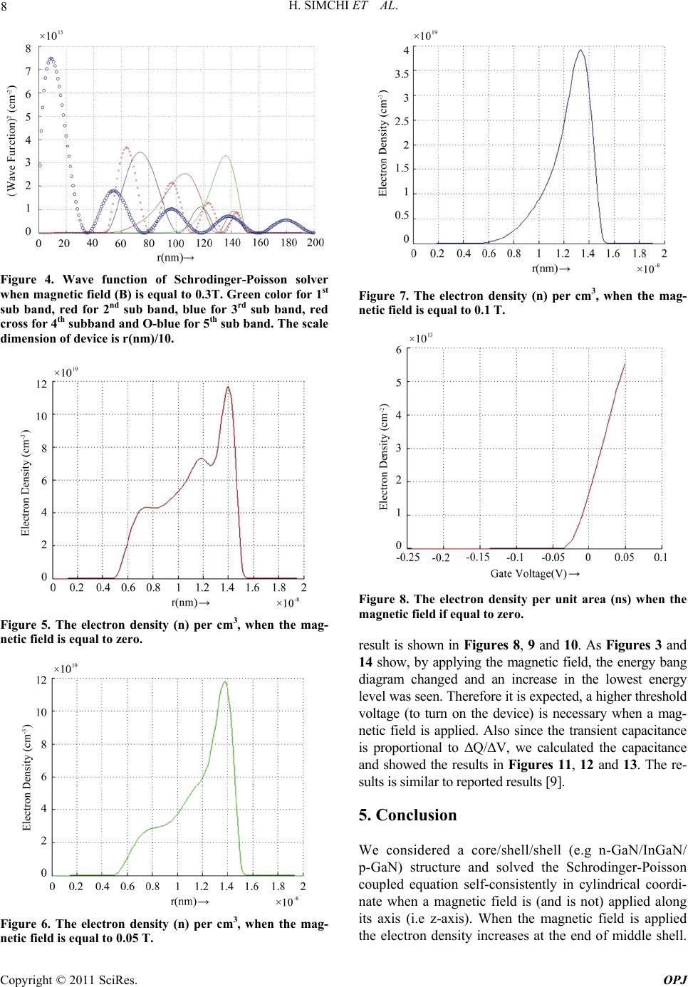 H. SIMCHI ET AL. Copyright © 2011 SciRes. OPJ 8 Figure 4. Wave function of Schrodinger-Poisson solver when magnetic field (B) is equal to 0.3T. Green color for 1st sub band, red for 2nd sub band, blue for 3rd sub band, red cross for 4th subband and O-blue for 5th sub band. The scale dimension of device is r(nm)/10. Figure 5. The electron density (n) per cm3, when the mag- netic field is equal to zero. Figure 6. The electron density (n) per cm3, when the mag- netic field is equal to 0.05 T. Figure 7. The electron density (n) per cm3, when the mag- netic field is equal to 0.1 T. Figure 8. The electron density per unit area (ns) when the magnetic field if equal to zero. result is shown in Figures 8, 9 and 10. As Figures 3 and 14 show, by applying the magnetic field, the energy bang diagram changed and an increase in the lowest energy level was seen. Therefore it is expected, a higher threshold voltage (to turn on the device) is necessary when a mag- netic field is applied. Also since the transient capacitance is proportional to ΔQ/ΔV, we calculated the capacitance and showed the results in Figures 11, 12 and 13. The re- sults is similar to reported results [9]. 5. Conclusion We considered a core/shell/shell (e.g n-GaN/InGaN/ p-GaN) structure and solved the Schrodinger-Poisson coupled equation self-consistently in cylindrical coordi- nate when a magnetic field is (and is not) applied along its axis (i.e z-axis). When the magnetic field is applied the electron density increases at the end of middle shell.  H. SIMCHI ET AL. Copyright © 2011 SciRes. OPJ 9 Figure 9. The electron density per unit area (ns) when the magnetic field if equal to 0.05 T. Figure 10. The electron density per unit area (ns) when the magnetic field if equal to 0.1 T. Figure 11. The capacitance via gate voltage, when the mag- netic field is equal to zero. Figure 12. The capacitance via gate voltage, when the mag- netic field is equal to 0.05 T. Figure 13. The capacitance via gate voltage when the mag- netic field is equal to 0.1 T. Figure 14. The eigenvalue via eigennumbers when the magnetic field is equal to zero (red color), 0.1 T (green color) and 0.3 T (blue color).  H. SIMCHI ET AL. Copyright © 2011 SciRes. OPJ 10 Therefore if we increase the magnetic field gradually, at a critical value, all electrons only moves on the outer surface of shell and one may make a nano-device which its electrons move only on its outer surface. Also it was shown the energy bang diagram changed and an increase in the lowest energy level was seen the magnetic field is applied. Therefore it is expected, a higher threshold voltage (to turn on the device) is necessary when a magnetic field is applied. The transient capacitance which is proportional to ΔQ/ΔV, was calculated. 6. References [1] L. J. Lauhon, M. S. Gudiksen, D. Wang and C. M. Lieber, “Epitaxial Core–Shell and Core–Multishell Nanowire Heterostructures,” Nature, Vol. 420, No. 6911, 2002, pp. 57-61. doi:10.1038/nature01141 [2] J. Goldberger et al. “Single-Crystal Gallium Nitride Na- notubes,” Nature, Vol. 422, No. 6932, 2003, pp. 599-602. doi:10.1038/nature01551 [3] F. Qian, Y. Li, S. Gradecak, D. Wang, C. J. Barrelet and C. M. Lieber , “Gallium Nitride-Based Nanowire Radial Heterostructures for Nanophotonics,” Nano letters, Vol. 4, No. 10, 2004, pp. 1975-1979. doi:10.1021/nl0487774 [4] F. Qian et al, “Core/Multishell Nanowire Heterostruc- tures as Multicolor, High-Efficiency Light-Emitting Dio- des,” Nano letters, Vol. 5, No. 11, 2005, pp. 2287-2291. doi:10.1021/nl051689e [5] Oliver Hayden et al, “Core-Shell Naowire Light-Emitting Diodes,” Advanced Materials, Vol. 17, No. 6, 2005, pp.701-704. doi:10.1002/adma.200401235 [6] Y. Dind et al, “Interface and Defect Structure of Zn-ZnO Core-Shell Heteronanobelts,” Journal of Applied Physics, Vol. 95, No. 1, 2004, p. 306. [7] T. Mokari and U. Banin, “Synthesis and properties of CdSe/ZnS Rod/Shell Nanocrystals,” Chemistry of Mate- rials, Vol. 15, No. 20, 2003, pp. 3955-3960. [8] Joachim Piprek et al, “Simulation and Optimization of 420 nm InGaN/GaN laser Diodes,” Proceedings of SPIE, Vol. 3944, 2000, p. 28. [9] L. Q. Wang et al, “A Numerical Schrodinger-Poisson Solver for Radially Symmetric Core-Shell Structures,” Solid-State Electronics, Vol. 50, No. 11-12, 2006, pp. 1732-1739. doi:10.1016/j.sse.2006.09.013 [10] Y. R. Wu, P. C. Yu, C. H. Chiu, C. Y. Chang and H. C. Kuo, “Analysis of Strain Relaxation and Emission Spec- trum of A Free-Standing GaN-based Nanopillar,” Pro- ceedings Of SPIE, Vol. 7058, 2008, pp. 7058G-7058G-10. doi:10.1117/12.800658 [11] F. Kootstra, P. L. de Boeij, H. Aissa and J. G. Snijders, “Relativistic Effects on the Optical Response of InSb by Time-Dependent Density-Functional Theory,” Journal of Chemical Physics, Vol. 114, No. 4, 2001, pp. 1860-1865. doi:10.1063/1.1334615 |