Paper Menu >>
Journal Menu >>
 Optics and Photonics Journal, 2011, 1, 1-4 doi:10.4236/ opj.2011.11001 Published Online March 2011 (http://www.SciRP.org/journal/opj) Copyright © 2011 SciRes. OPJ Investigation of the Optical Properties of CdBr2 Hamdollah Salehi, Nastaran Asareh Department of Physics, Shahid Chamran University of Ahvaz, Ahvaz, Iran E-mail: salehi_h@sua.ac.ir Received Feburary 13, 2011; revised Feburary 28, 2011; accepted March 7, 2011 Abstract The optical properties of CdBr2 were studied by first principle using the density functional theory. The di- electric functions and optical constants are calculated using the full potential-linearized augmented plane wave (FP-LAPW) method with the generalized gradient approximation (GGA). The theoretical calculated optical properties and energy Loss (EEL) spectrum yield a static refractive index of 2.1 and a plasmon ener- gy of 13eV for hexagonal phase. The results, in comparison with the published data, are in good agreement with the experimental and previous theoretical results. Keywords: Optical Properties, CdBr2, WIEN2k, FP-LAPW, DFT, GGA 1. Introduction Cadmium halogenides are widely uses as radiations. The lattice of these complicated crystals are strongly anisotropic. The CdBr2 structure is of the CdCl2 type, namely, the rhombic lattice with 5 3d D symmetry [1]. Cadmium bromide Crystallise with layer structures in which band- ing within the layer is strong with a large ionic contribu- tion, while bonding between the layers is weak. The ba- sic structure of these materials is an infinite hexagonal sheet of Cd atoms sandwiched between two similar sheets of halogen atoms, the Cd atoms being Octahe- drally coordinated. These three-sheet sandwiches (or layers) are then stacked to form the three-dimensional compound. Because of the weak binding between the layers, different stacking sequences represent only slight differences in total energy and so several such sequences are possible. There is relatively little information availa- ble about the electronic and optical properties of the cadmium halides as a whole. Band structure calculations have recently been made for CdI, (McCanny et al 1977, Bordas et al 1978, Robertson 1979). Optical experiments in the main have been concerned with the strong excitons exhibited by all three materials [2]. Cadmium bromide is known as a photochromic crystal and is widely used as window for Infrared applications [3]. In the present work the optical properties of CdBr2 have been studied using the full potential linearized augmented plane wave method (FP-LAPW). The results, in compari- son with the published data, are in good agreement with the experimental and previous theoretical results. 2. Method of Calculation Calculation of the optical properties, of CdBr2 were car- ried out with a self-consistent scheme by solving the Kohn-Sham equation using a FP-LAPW method in the framework of the DFT along with the GGA method [4,5] by WIEN2k package [6]. In the FP-LAPW method, space is divided into two regions, a spherical “muf- fin-tin” around the nuclei in which radial solutions of Schrödinger Equation and their energy derivatives are used as basis functions, and an “interstitial” region be- tween the muffin tins (MT) in which the basis set con- sists of plane waves. There is no pseudopotential ap- proximation and core states are calculated selfconsis- tently in the crystal potential. Also, core states are treated fully relativistically while valence and semi-core states are treated semi-relativistically (i.e. ignoring the spin orbit coupling). The cut-off energy, which defines the separation of the core and valance states, was chosen as –6 Ryd. The complex dielectric tensor was calculated, in this program, according to the well-known relations [7]. 2 αβ cv 22 c,v 4πe Imdkc|p|vv|p |cδεεω mω kk kkkk (1) 22 0 Im 2 Re πPd (2) and the optical conductivity is given by: 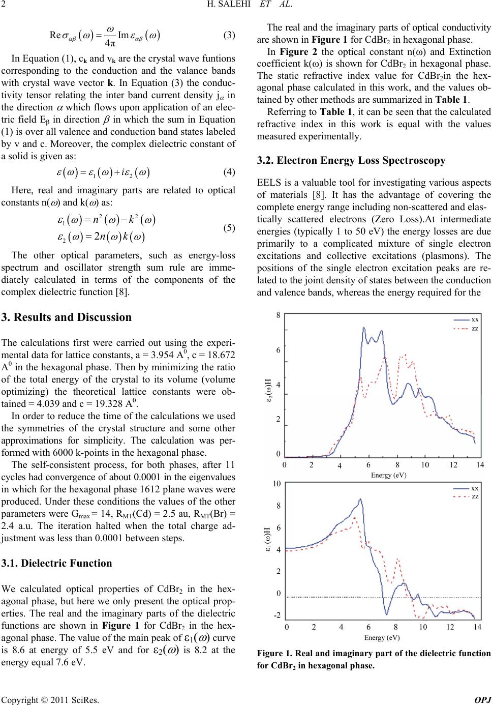 2 H. SALEHI ET AL. Copyright © 2011 SciRes. OPJ Re Im 4π (3) In Equation (1), ck and vk are the crystal wave funtions corresponding to the conduction and the valance bands with crystal wave vector k. In Equation (3) the conduc- tivity tensor relating the inter band current density j in the direction which flows upon application of an elec- tric field E in direction in which the sum in Equation (1) is over all valence and conduction band states labeled by v and c. Moreover, the complex dielectric constant of a solid is given as: 12 i (4) Here, real and imaginary parts are related to optical constants n( ) and k( ) as: 22 1 22 nk nk (5) The other optical parameters, such as energy-loss spectrum and oscillator strength sum rule are imme- diately calculated in terms of the components of the complex dielectric function [8]. 3. Results and Discussion The calculations first were carried out using the experi- mental data for lattice constants, a = 3.954 A0, c = 18.672 A0 in the hexagonal phase. Then by minimizing the ratio of the total energy of the crystal to its volume (volume optimizing) the theoretical lattice constants were ob- tained = 4.039 and c = 19.328 A0. In order to reduce the time of the calculations we used the symmetries of the crystal structure and some other approximations for simplicity. The calculation was per- formed with 6000 k-points in the hexagonal phase. The self-consistent process, for both phases, after 11 cycles had convergence of about 0.0001 in the eigenvalues in which for the hexagonal phase 1612 plane waves were produced. Under these conditions the values of the other parameters were Gmax = 14, RMT(Cd) = 2.5 au, RMT(Br) = 2.4 a.u. The iteration halted when the total charge ad- justment was less than 0.0001 between steps. 3.1. Dielectric Function We calculated optical properties of CdBr2 in the hex- agonal phase, but here we only present the optical prop- erties. The real and the imaginary parts of the dielectric functions are shown in Figure 1 for CdBr2 in the hex- agonal phase. The value of the main peak of 1( ) curve is 8.6 at energy of 5.5 eV and for 2( ) is 8.2 at the energy equal 7.6 eV. The real and the imaginary parts of optical conductivity are shown in Figure 1 for CdBr2 in hexagonal phase. In Figure 2 the optical constant n() and Extinction coefficient k() is shown for CdBr2 in hexagonal phase. The static refractive index value for CdBr2in the hex- agonal phase calculated in this work, and the values ob- tained by other methods are summarized in Table 1. Referring to Table 1 , it can be seen that the calculated refractive index in this work is equal with the values measured experimentally. 3.2. Electron Energy Loss Spectroscopy EELS is a valuable tool for investigating various aspects of materials [8]. It has the advantage of covering the complete energy range including non-scattered and elas- tically scattered electrons (Zero Loss).At intermediate energies (typically 1 to 50 eV) the energy losses are due primarily to a complicated mixture of single electron excitations and collective excitations (plasmons). The positions of the single electron excitation peaks are re- lated to the joint density of states between the conduction and valence bands, whereas the energy required for the Figure 1. Real and imaginary part of the dielectric function for CdBr2 in hexagonal phase. 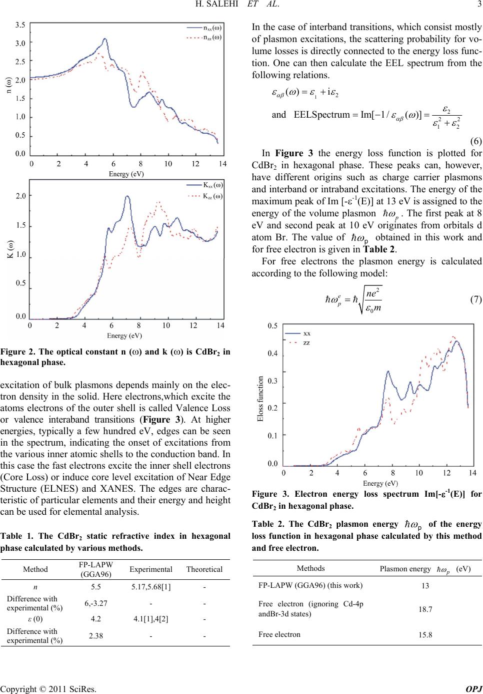 H. SALEHI ET AL. 3 Copyright © 2011 SciRes. OPJ Figure 2. The optical constant n () and k () is CdBr2 in hexagonal phase. excitation of bulk plasmons depends mainly on the elec- tron density in the solid. Here electrons,which excite the atoms electrons of the outer shell is called Valence Loss or valence interaband transitions (Figure 3). At higher energies, typically a few hundred eV, edges can be seen in the spectrum, indicating the onset of excitations from the various inner atomic shells to the conduction band. In this case the fast electrons excite the inner shell electrons (Core Loss) or induce core level excitation of Near Edge Structure (ELNES) and XANES. The edges are charac- teristic of particular elements and their energy and height can be used for elemental analysis. Table 1. The CdBr2 static refractive index in hexagonal phase calculated by various methods. Method FP-LAPW (GGA96) Experimental Theoretical n 5.5 5.17,5.68[1] - Difference with experimental (%) 6,-3.27 - - ε (0) 4.2 4.1[1],4[2] - Difference with experimental (%) 2.38 - - In the case of interband transitions, which consist mostly of plasmon excitations, the scattering probability for vo- lume losses is directly connected to the energy loss func- tion. One can then calculate the EEL spectrum from the following relations. 12 2 22 12 ()i and EELSpectrumIm[1/()] (6) In Figure 3 the energy loss function is plotted for CdBr2 in hexagonal phase. These peaks can, however, have different origins such as charge carrier plasmons and interband or intraband excitations. The energy of the maximum peak of Im [--1(E)] at 13 eV is assigned to the energy of the volume plasmon p . The first peak at 8 eV and second peak at 10 eV originates from orbitals d atom Br. The value of p obtained in this work and for free electron is given in Table 2. For free electrons the plasmon energy is calculated according to the following model: 2 0 e p ne m (7) Figure 3. Electron energy loss spectrum Im[--1(E)] for CdBr2 in hexagonal phase. Table 2. The CdBr2 plasmon energy p of the energy loss function in hexagonal phase calculated by this method and free electron. Methods Plasmon energy p (eV) FP-LAPW (GGA96) (this work)13 Free electron (ignoring Cd-4p andBr-3d states) 18.7 Free electron 15.8 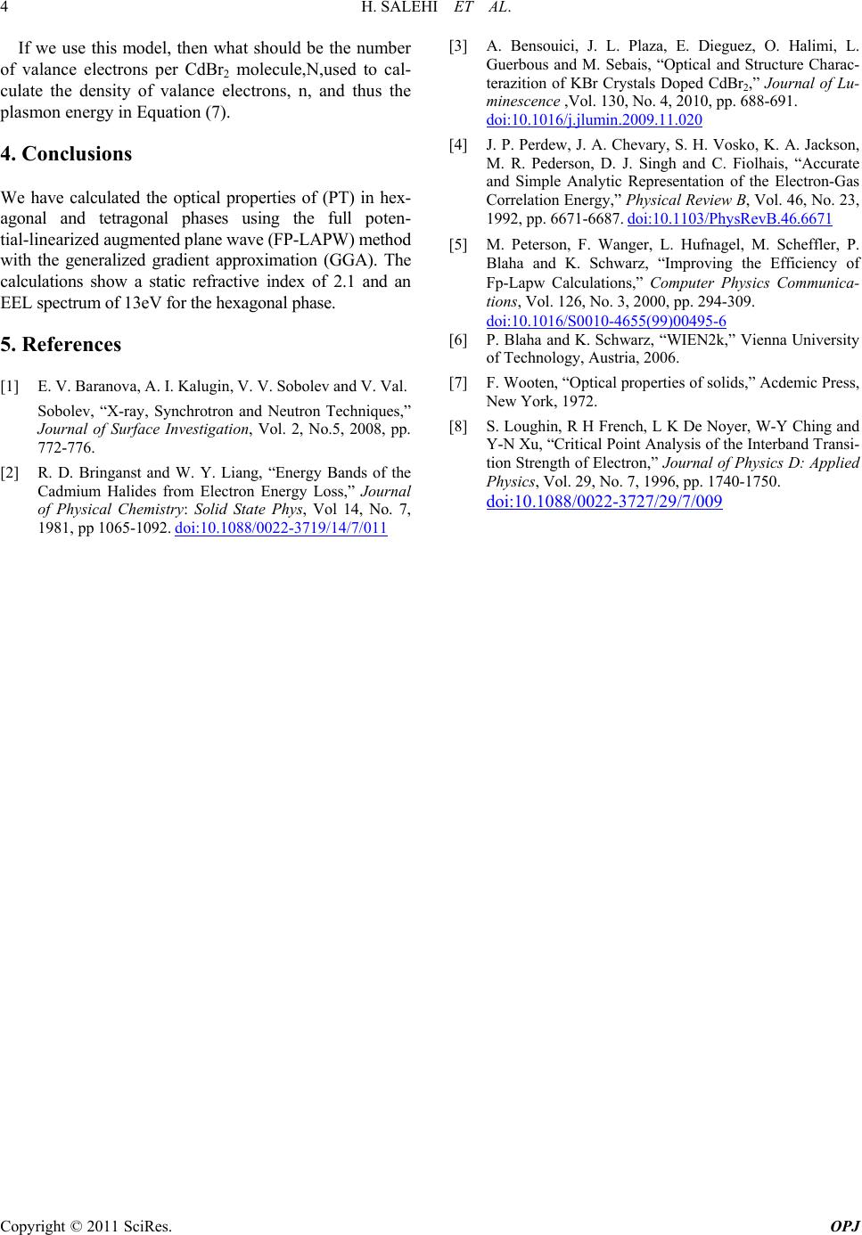 4 H. SALEHI ET AL. Copyright © 2011 SciRes. OPJ If we use this model, then what should be the number of valance electrons per CdBr2 molecule,N,used to cal- culate the density of valance electrons, n, and thus the plasmon energy in Equation (7). 4. Conclusions We have calculated the optical properties of (PT) in hex- agonal and tetragonal phases using the full poten- tial-linearized augmented plane wave (FP-LAPW) method with the generalized gradient approximation (GGA). The calculations show a static refractive index of 2.1 and an EEL spectrum of 13eV for the hexagonal phase. 5. References [1] E. V. Baranova, A. I. Kalugin, V. V. Sobolev and V. Val. Sobolev, “X-ray, Synchrotron and Neutron Techniques,” Journal of Surface Investigation, Vol. 2, No.5, 2008, pp. 772-776. [2] R. D. Bringanst and W. Y. Liang, “Energy Bands of the Cadmium Halides from Electron Energy Loss,” Journal of Physical Chemistry: Solid State Phys, Vol 14, No. 7, 1981, pp 1065-1092. doi:10.1088/0022-3719/14/7/011 [3] A. Bensouici, J. L. Plaza, E. Dieguez, O. Halimi, L. Guerbous and M. Sebais, “Optical and Structure Charac- terazition of KBr Crystals Doped CdBr2,” Journal of Lu- minescence ,Vol. 130, No. 4, 2010, pp. 688-691. doi:10.1016/j.jlumin.2009.11.020 [4] J. P. Perdew, J. A. Chevary, S. H. Vosko, K. A. Jackson, M. R. Pederson, D. J. Singh and C. Fiolhais, “Accurate and Simple Analytic Representation of the Electron-Gas Correlation Energy,” Physical Review B, Vol. 46, No. 23, 1992, pp. 6671-6687. doi:10.1103/PhysRevB.46.6671 [5] M. Peterson, F. Wanger, L. Hufnagel, M. Scheffler, P. Blaha and K. Schwarz, “Improving the Efficiency of Fp-Lapw Calculations,” Computer Physics Communica- tions, Vol. 126, No. 3, 2000, pp. 294-309. doi:10.1016/S0010-4655(99)00495-6 [6] P. Blaha and K. Schwarz, “WIEN2k,” Vienna University of Technology, Austria, 2006. [7] F. Wooten, “Optical properties of solids,” Acdemic Press, New York, 1972. [8] S. Loughin, R H French, L K De Noyer, W-Y Ching and Y-N Xu, “Critical Point Analysis of the Interband Transi- tion Strength of Electron,” Journal of Physics D: Applied Physics, Vol. 29, No. 7, 1996, pp. 1740-1750. doi:10.1088 /0022-3727 /29/7/009 |