Paper Menu >>
Journal Menu >>
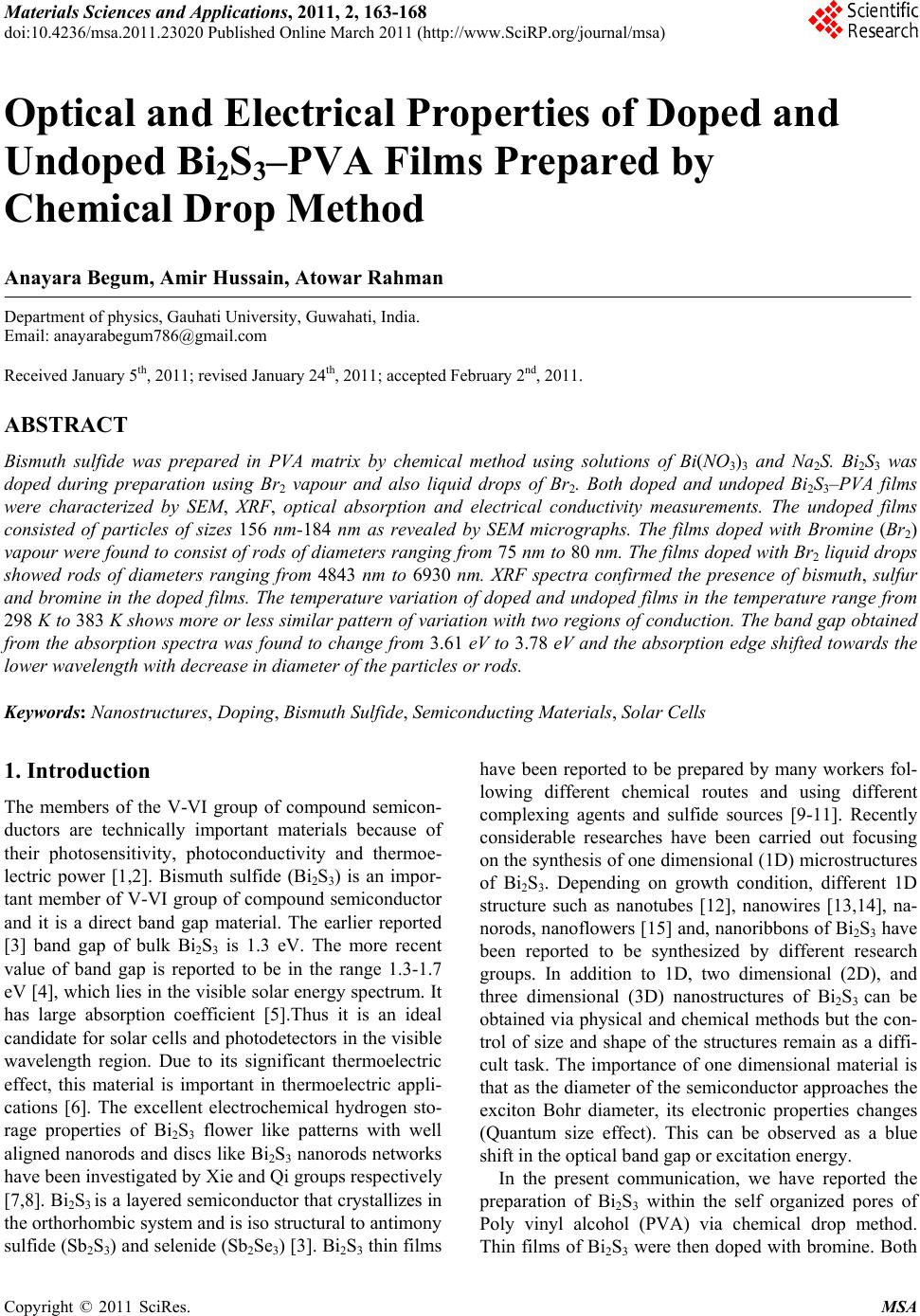 Materials Sciences and Applications, 2011, 2, 163-168 doi:10.4236/msa.2011.23020 Published Online March 2011 (http://www.SciRP.org/journal/msa) Copyright © 2011 SciRes. MSA Optical and Electrical Properties of Doped and Undoped Bi2S3–PVA Films Prepared by Chemical Drop Method Anayara Begum, Amir Hussain, Atowar Rahman Department of physics, Gauhati University, Guwahati, India. Email: anayarabegum786@gmail.com Received January 5th, 2011; revised January 24th, 2011; accepted February 2nd, 2011. ABSTRACT Bismuth sulfide was prepared in PVA matrix by chemical method using solutions of Bi(NO3)3 and Na2S. Bi2S3 was doped during preparation using Br2 vapour and also liquid drops of Br2. Both doped and undoped Bi2S3–PVA films were characterized by SEM, XRF, optical absorption and electrical conductivity measurements. The undoped films consisted of particles of sizes 156 nm-184 nm as revealed by SEM micrographs. The films doped with Bromine (Br2) vapour were found to consist of rods of diameters ranging from 75 nm to 80 nm. The films doped with Br2 liquid drops showed rods of diameters ranging from 4843 nm to 6930 nm. XRF spectra confirmed the presence of bismuth, sulfur and bromine in the doped films. The temperature variation of doped and undoped films in the temperature range from 298 K to 383 K shows more or less similar pattern of variation with two regions of conduction. The band gap obtained from the absorption spectra was found to change from 3.61 eV to 3.78 eV and the absorption edge shifted towards the lower wavelength with decrease in diameter of the particles or rods. Keywords: Nanostructures, Doping, Bismuth Sulfide, Semiconducting Materials, Solar Cells 1. Introduction The members of the V-VI group of compound semicon- ductors are technically important materials because of their photosensitivity, photoconductivity and thermoe- lectric power [1,2]. Bismuth sulfide (Bi2S3) is an impor- tant member of V-VI group of compound semiconductor and it is a direct band gap material. The earlier reported [3] band gap of bulk Bi2S3 is 1.3 eV. The more recent value of band gap is reported to be in the range 1.3-1.7 eV [4], which lies in the visible solar energy spectrum. It has large absorption coefficient [5].Thus it is an ideal candidate for solar cells and photodetectors in the visible wavelength region. Due to its significant thermoelectric effect, this material is important in thermoelectric appli- cations [6]. The excellent electrochemical hydrogen sto- rage properties of Bi2S3 flower like patterns with well aligned nanorods and discs like Bi2S3 nanorods networks have been investigated by Xie and Qi groups respectively [7,8]. Bi2S3 is a layered semiconductor that crystallizes in the orthorhombic system and is iso structural to antimony sulfide (Sb2S3) and selenide (Sb2Se3) [3]. Bi2S3 thin films have been reported to be prepared by many workers fol- lowing different chemical routes and using different complexing agents and sulfide sources [9-11]. Recently considerable researches have been carried out focusing on the synthesis of one dimensional (1D) microstructures of Bi2S3. Depending on growth condition, different 1D structure such as nanotubes [12], nanowires [13,14], na- norods, nanoflowers [15] and, nanoribbons of Bi2S3 have been reported to be synthesized by different research groups. In addition to 1D, two dimensional (2D), and three dimensional (3D) nanostructures of Bi2S3 can be obtained via physical and chemical methods but the con- trol of size and shape of the structures remain as a diffi- cult task. The importance of one dimensional material is that as the diameter of the semiconductor approaches the exciton Bohr diameter, its electronic properties changes (Quantum size effect). This can be observed as a blue shift in the optical band gap or excitation energy. In the present communication, we have reported the preparation of Bi2S3 within the self organized pores of Poly vinyl alcohol (PVA) via chemical drop method. Thin films of Bi2S3 were then doped with bromine. Both 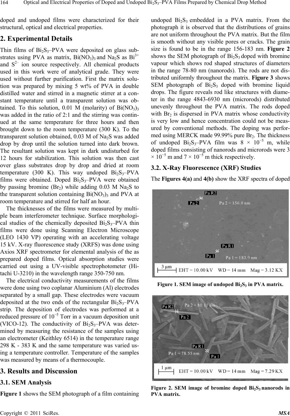 Optical and Electrical Properties of Doped and Undoped Bi2S3–PVA Films Prepared by Chemical Drop Method Copyright © 2011 SciRes. MSA 164 doped and undoped films were characterized for their structural, optical and electrical properties. 2. Experimental Details Thin films of Bi2S3–PVA were deposited on glass sub- strates using PVA as matrix, Bi(NO3)3 and Na2S as Bi3+ and S2– ion source respectively. All chemical products used in this work were of analytical grade. They were used without further purification. First the matrix solu- tion was prepared by mixing 5 wt% of PVA in double distilled water and stirred in a magnetic stirrer at a con- stant temperature until a transparent solution was ob- tained. To this solution, 0.01 M (molarity) of Bi(NO3)3 was added in the ratio of 2:1 and the stirring was contin- ued at the same temperature for three hours and then brought down to the room temperature (300 K). To the transparent solution obtained, 0.03 M of Na2S was added drop by drop until the solution turned into dark brown. The resultant solution was kept in dark undisturbed for 12 hours for stabilization. This solution was then cast over glass substrates drop by drop and dried at room temperature (300 K). This way undoped Bi2S3–PVA films were obtained. Doped Bi2S3–PVA were obtained by passing bromine (Br2) while adding 0.03 M Na2S to the transparent solution containing Bi(NO3)3 and PVA at room temperature and stirred for half an hour. The thicknesses of the films were measured by multi- ple beam interferometer technique. Surface morphologi- cal studies of the chemically deposited Bi2S3–PVA thin films were done using Scanning Electron Microscope (LEO 1430 VP) operating with an accelerating voltage 15 kV. X-ray fluorescence study (XRFS) was done using Axios XRF spectrometer for elemental analysis of the as prepared doped films. Optical absorption studies were carried out using a UV-visible spectrophotometer (Hi- tachi U-3210) in the wavelength range 350-750 nm. The electrical conductivity measurements of the films were done using two coplanar Aluminium (Al) electrodes separated by a small gap. These electrodes were vacuum deposited at the two ends of the rectangular Bi2S3–PVA strip. The deposition of electrodes was performed at a reduced pressure of 10−5 Torr in a vacuum deposition unit (VICO-12). The conductivity of Bi2S3–PVA was deter- mined by measuring the resistance of the samples using an electrometer (Keithley 6514) in the temperature range 298 K - 383 K and the same temperature was varied us- ing a temperature controller. Temperature of the samples was measured by means of a thermocouple. 3. Results and Discussion 3.1. SEM Analysis Figure 1 shows the SEM photograph of a film containing undoped Bi2S3 embedded in a PVA matrix. From the photograph it is observed that the distributions of grains are not uniform throughout the PVA matrix. But the film is smooth without any visible pores or cracks. The grain size is found to be in the range 156-183 nm. Figure 2 shows the SEM photograph of Bi2S3 doped with bromine vapour which shows rod shaped structures of diameters in the range 78-80 nm (nanorods). The rods are not dis- tributed uniformly throughout the matrix. Figure 3 shows SEM photograph of Bi2S3 doped with bromine liquid drops. The figure reveals rod like structures with diame- ter in the range 4843-6930 nm (microrods) distributed unevenly throughout the PVA matrix. The rods doped with Br2 is dispersed in PVA matrix whose conductivity is very low and hence concentration could not be meas- ured by conventional methods. The doping was perfor- med using MERCK made 99.99% pure Br2. The thickness of undoped Bi2S3–PVA film was 8 × 10⁻⁵ m, while doped films consisting of nanorods and microrods were 3 × 10⁻⁵ m and 7 × 10⁻⁵ m thick respectively. 3.2. X-Ray Fluorescence (XRF) Studies The Figures 4(a) and 4(b) show the XRF spectra of doped Figure 1. SEM image of undope d Bi 2S3 in PVA matrix. Figure 2. SEM image of bromine doped Bi2S3 nanorods in PVA matrix. 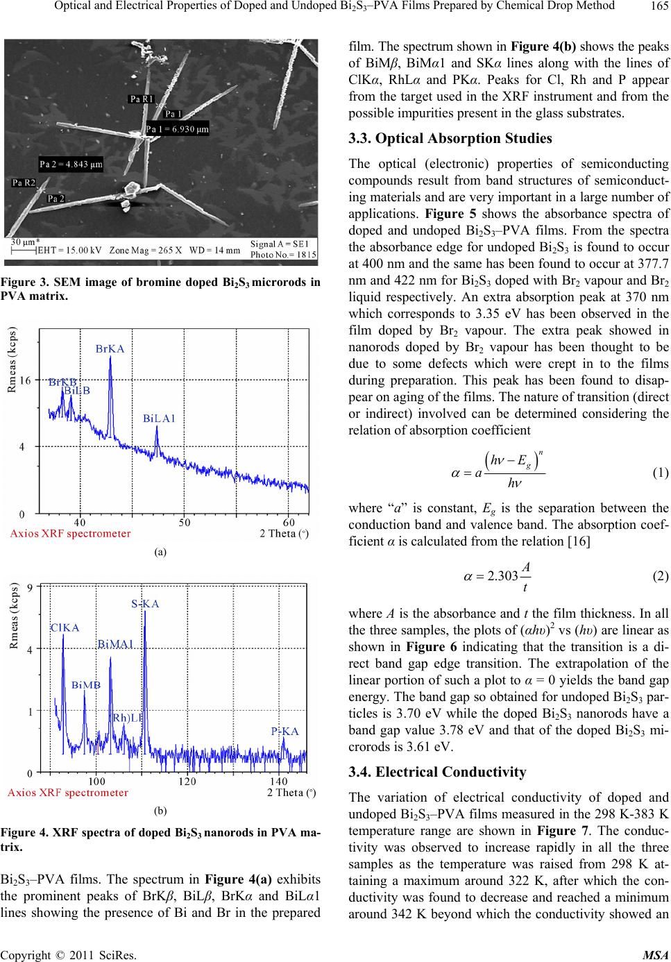 Optical and Electrical Properties of Doped and Undoped Bi2S3–PVA Films Prepared by Chemical Drop Method Copyright © 2011 SciRes. MSA 165 Figure 3. SEM image of bromine doped Bi2S3 microrods in PVA matrix. (a) (b) Figure 4. XRF spectra of doped Bi2S3 nanorods in PVA ma- trix. Bi2S3–PVA films. The spectrum in Figure 4(a) exhibits the prominent peaks of BrKβ, BiLβ, BrKα and BiLα1 lines showing the presence of Bi and Br in the prepared film. The spectrum shown in Figure 4(b) shows the peaks of BiMβ, BiMα1 and SKα lines along with the lines of ClKα, RhLα and PKα. Peaks for Cl, Rh and P appear from the target used in the XRF instrument and from the possible impurities present in the glass substrates. 3.3. Optical Absorption Studies The optical (electronic) properties of semiconducting compounds result from band structures of semiconduct- ing materials and are very important in a large number of applications. Figure 5 shows the absorbance spectra of doped and undoped Bi2S3–PVA films. From the spectra the absorbance edge for undoped Bi2S3 is found to occur at 400 nm and the same has been found to occur at 377.7 nm and 422 nm for Bi2S3 doped with Br2 vapour and Br2 liquid respectively. An extra absorption peak at 370 nm which corresponds to 3.35 eV has been observed in the film doped by Br2 vapour. The extra peak showed in nanorods doped by Br2 vapour has been thought to be due to some defects which were crept in to the films during preparation. This peak has been found to disap- pear on aging of the films. The nature of transition (direct or indirect) involved can be determined considering the relation of absorption coefficient n g hE ah (1) where “a” is constant, Eg is the separation between the conduction band and valence band. The absorption coef- ficient α is calculated from the relation [16] 2.303 A t (2) where A is the absorbance and t the film thickness. In all the three samples, the plots of (αhυ)2 vs (hυ) are linear as shown in Figure 6 indicating that the transition is a di- rect band gap edge transition. The extrapolation of the linear portion of such a plot to α = 0 yields the band gap energy. The band gap so obtained for undoped Bi2S3 par- ticles is 3.70 eV while the doped Bi2S3 nanorods have a band gap value 3.78 eV and that of the doped Bi2S3 mi- crorods is 3.61 eV. 3.4. Electrical Conductivity The variation of electrical conductivity of doped and undoped Bi2S3–PVA films measured in the 298 K-383 K temperature range are shown in Figure 7. The conduc- tivity was observed to increase rapidly in all the three samples as the temperature was raised from 298 K at- taining a maximum around 322 K, after which the con- ductivity was found to decrease and reached a minimum around 342 K beyond which the conductivity showed an 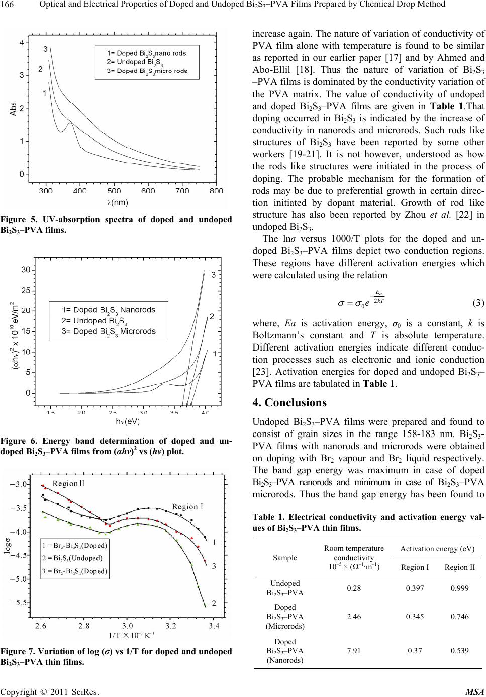 Optical and Electrical Properties of Doped and Undoped Bi2S3–PVA Films Prepared by Chemical Drop Method Copyright © 2011 SciRes. MSA 166 Figure 5. UV-absorption spectra of doped and undoped Bi2S3–PVA films. Figure 6. Energy band determination of doped and un- doped Bi2S3–PVA films from (αhν)2 vs (hν) plot. Figure 7. Variation of log (σ) vs 1/T for doped and undoped Bi2S3–PVA thin films. increase again. The nature of variation of conductivity of PVA film alone with temperature is found to be similar as reported in our earlier paper [17] and by Ahmed and Abo-Ellil [18]. Thus the nature of variation of Bi2S3 –PVA films is dominated by the conductivity variation of the PVA matrix. The value of conductivity of undoped and doped Bi2S3–PVA films are given in Table 1.That doping occurred in Bi2S3 is indicated by the increase of conductivity in nanorods and microrods. Such rods like structures of Bi2S3 have been reported by some other workers [19-21]. It is not however, understood as how the rods like structures were initiated in the process of doping. The probable mechanism for the formation of rods may be due to preferential growth in certain direc- tion initiated by dopant material. Growth of rod like structure has also been reported by Zhou et al. [22] in undoped Bi2S3. The lnσ versus 1000/T plots for the doped and un- doped Bi2S3–PVA films depict two conduction regions. These regions have different activation energies which were calculated using the relation 2 0 a E kT e (3) where, Ea is activation energy, σ0 is a constant, k is Boltzmann’s constant and T is absolute temperature. Different activation energies indicate different conduc- tion processes such as electronic and ionic conduction [23]. Activation energies for doped and undoped Bi2S3– PVA films are tabulated in Table 1. 4. Conclusions Undoped Bi2S3–PVA films were prepared and found to consist of grain sizes in the range 158-183 nm. Bi2S3- PVA films with nanorods and microrods were obtained on doping with Br2 vapour and Br2 liquid respectively. The band gap energy was maximum in case of doped Bi2S3–PVA nanorods and minimum in case of Bi2S3–PVA microrods. Thus the band gap energy has been found to Table 1. Electrical conductivity and activation energy val- ues of Bi2S3–PVA thin films. Activation energy (eV) Sample Room temperature conductivity 10–5 × (Ω–1·m–1) Region I Region II Undoped Bi2S3–PVA 0.28 0.397 0.999 Doped Bi2S3–PVA (Microrods) 2.46 0.345 0.746 Doped Bi2S3–PVA (Nanorods) 7.91 0.37 0.539  Optical and Electrical Properties of Doped and Undoped Bi2S3–PVA Films Prepared by Chemical Drop Method Copyright © 2011 SciRes. MSA 167 increase with decrease in size showing a blue shift in the absorption spectra. On doping there was an increase in the electrical conductivity of Bi2S3–PVA films. However the conductivity of all the samples was largely influenced by the conductivity of PVA structure. 5. Acknowledgements The authors express their gratefulness to the Department of Chemistry, Gauhati University, Guwahati and IIT Gu- wahati for providing us the UV-Visible Spectra and SEM facilities respectively. REFERENCES [1] C. Ghosh and B. P. Varma, “Optical Properties of Amor- phous and Crystalline Sb2S3 Thin Films,” Thin solid films, Vol. 60, No. 1, June 1979, pp. 61-65. doi:10.1016/0040-6090(79)90347-X [2] C. Ghosh and B. P. Varma, “Some Optical Properties of Amorphous and Crystalline Antimony Trisulphide Thin Films,” Solid State Communications, Vol. 31, No. 9, Sep- tember 1979, pp. 683-686. [3] J. Black, E. M. Conwell, L. Seigle and C. W. Spenser, “Electrical and Optical Properties of Some M2 V-B N 3 VI-B Semicopnductors,” Journal of Physics and Chemistry of Solids, Vol. 2, 1957, pp. 240-251. doi:10.1016/0022-3697(57)90090-2 [4] D. J. Riley, J. P. Waggett and K. G. U. Wijayantha, “Colloidal Bismuth Sulfide Nanoparticles: A Photoelec- trochemical Study of the Relationship between Bandgap and Particle Size,” Journal of Materials Chemistry, Vol. 14, November 2003, pp. 704-708. [5] L. Cademartiri, R. Malakooti, P. G. O’Brien, A. Migliori, S. Petrov, N. Kherani and G. A. Ozin, “Large Scale Syn- thesis of Ultrathin Bi2S3 Necklace Nanowires,” Ange- wandte Chemie International Edition, Vol. 20, 2008, pp. 3814-3817. [6] O. Rabin, J. M. Perez, J. Grimm, G. Wojtkiewicz and R. Weissleder, “An X-Ray Computed Tomography Imaging Agent Based on Long-Circulating Bismuth Sulphide Nanoparticles,” Nature Materials, Vol. 5, No. 2, 2006, pp. 118-122. doi:10.1038/nmat1571 [7] B. Zhang, X. C. Ye, W. Y. Hou, Y. Zhao and Y. Xie, “Biomolecule-Assisted Synthesis and Electrochemical Hydrogen Storage of Bi2S3 Flowerlike Patterns with Well Aligned Nanorods,” Journal of Physical Chemistry B, Vol. 110, No. 18, 2006, pp. 8978-8985. doi:10.1021/jp060769j [8] L. S. Li, N. J. Sun, Y. Y. Huang, Y. Qin, N. N. Zhao, J. N. Gao, M. X. Li, H. H. Zhou and L. M. Qi, “Topotactic Transformation of Single-Crystalline Precursor Discs into Disc-Like Bi2S3 Nanorod Networks,” Advance Func- tional Matererials, Vol. 18, No. 8, 2008, pp. 1194-1201. doi:10.1002/adfm.200701467 [9] S. Biswas, A. Mondal, D. Mukherjee and P. Pramanik, “A Chemical Method for the Deposition of Bismuth Sul- fide Thin Films,” Journal of Electrochemical Society, Vol. 133, No. 1, January 1986, pp. 48-52. doi:10.1149/1.2108539 [10] P. Pramanik and R. N. Bhattacharya, “A Chemical Method for Deposition of Thin Film of Bi2S3,” Journal of Electrochemical Society, Vol. 127, No. 9, 1980, p. 2087. doi:10.1149/1.2130072 [11] J. D. Desai and C. D. Lokhande, “Chemical Deposition of Bi2S3 Thin Films from Thioacetamide Bath,” Materials Chemistry and Physics, Vol. 41, 1995, pp. 98-103. doi:10.1016/0254-0584(95)01538-8 [12] P. A. K. Moorthy, “Formation of Stoichiometric Bismuth Trisulphide Compound Films,” Journal of Materials Sci- ence Letters, Vol. 3, No. 9, 1984, pp. 837-839. doi:10.1007/BF00727989 [13] D. S. Wang, C. H. Hao, W. Zheng, X. L. Ma, D. R. Chu, Q. Peng and Y. D. Li, “Bi2S3 Nanotubes: Facile Synthesis and Growth Mechanism,” Nano Research, Vol. 2, No. 2, 2009, pp. 130-134. doi:10.1007/s12274-009-9010-2 [14] H. F. Bao, X. Q. Cui, C. M. Li, Y. Gan, J. Zhang and J. Guo, “Photoswitchable Semiconductor Bismuth Sulfide (Bi2S3) Nanowires and Their Self-Supported Nanowires arrays,” Journal of Physical Chemistry C, Vol. 111, No. 33, June 2007, pp. 12279-12283. doi:10.1021/jp073504t [15] X. L. Yu and C. B. Cao, “Photoresponse and Field-Emission Properties of Bismuth Sulfide Nanoflowers,” Crystal Growth & Design, Vol. 8, No. 11, September 2008, pp. 3951-3955. doi:10.1021/cg701001m [16] J. Barman, K. C. Sarma, M. Sarma and K. Sarma, “Struc- tural and Optical Studies of Chemically Prepared CdS Nanocrystalline Thin Films,” Indian Journal of Pure and Applied Physics, Vol. 46, No. 5, May 2008, pp. 339-343. [17] A. Hussain. A. Begum, and A. Rahman, “Optical and Electrical Properties of Bismuth Sulfide Thin Films Pre- pared in PVA Matrix by Chemical Drop Method,” Jour- nal of Optoelectronics and Advanced Materials, Vol. 12, No. 5, May 2010, pp. 1019-1023. [18] M. A. Ahmed and M. S. Abo-Ellil, “Effect of Dopant Concentration on the Electrical Properties of Polyvinyl Alcohol (PVA),” Journal of Materials Science: Materials in Electronics, Vol. 9, No. 5, 1998, pp. 391-395. doi:10.1023/A:1008944411984 [19] R. Chen, M.-H. So, C.-M. Che and H. Z. Sun, “Con- trolled Synthesis of High Crystalline Bismuth Sulfide nanorods: Using Bismuth Citrate as a Precursor,” Journal of Material Cheistry, Vol. 15, No. 42, 2005, pp. 4540- 4545. doi:10.1039/b510299e [20] S.-H. Yu, J. Yang, Y.-S. Wu, Z.-H. Han, Y. Xie, Y.-T. Qian, “Hydrothermal Preparation and Characterization of Rod-Like Ultrafine Powders of Bismuth Sulfide,” Mate- rials Research Bulletin, Vol. 33, No. 11, November 1998, pp. 1661-1666. doi:10.1016/S0025-5408(98)00161-5 [21] J. M. Zhu, K. Yang, J. J. Zhu, G. B. Ma, X. H. Zhu, S. H. Zhou and Z. G. Liu, “The Microstructure Studies of Bis- muth Sulfide Nanorods Prepared by Sonochemical Method,” Materials Letters, Vol. 63, No. 17, July 2009, pp. 1496-1498. [22] S. X. Zhou, J. M. Li, Y. X. Ke and S. M. Lu, “Synthesis  Optical and Electrical Properties of Doped and Undoped Bi2S3–PVA Films Prepared by Chemical Drop Method Copyright © 2011 SciRes. MSA 168 of Bismuth Sulfide Nanorods in Acidic Media at Room Temperature,” Materials Letters, Vol. 57, No. 16-17, May 2003, pp. 2602-2605. doi:10.1016/S0167-577X(02)01334-4 [23] K. C. Kao and W. H. Wang, “Electrical Transport in Sol- ids,” Pergamon Press, Oxford, 1981. |