Journal of Computer and Communications, 2013, 1, 72-77
Published Online December 2013 (http://www.scirp.org/journal/jcc)
http://dx.doi.org/10.4236/jcc.2013.17017
Open Access JCC
Photonics from Al-Haitham to Optoelectronics of AMTEC
M. A. K. Lodhi
University of Management and Technology Lahore, Pakistan and Department of Physics, Texas Tech University Lubbock, TX 79409,
USA.
Email: a.lodhi@ttu.edu
Received 2013
ABSTRACT
The wordphotonicsis derived from the Greek word “photosmeaning light. It covers all technical applications of
light over the whole spectrum. Most applications, however, are in the range of the visible and near infrared light. With a
brief history of classical work and tenets of optics, we will present electrical circuit of a thin-film device used in a fuel
cell, called Alkali Metal Thermo Electric Convertor (AMTEC).The device uses infrared radiation to knock out electrons
from some alkali metal, which after going through a circuit and having done the prescribed work, meet the ions again.
The system is closed and continues work i ng as long as the radiation source is kept on. The longevity, power and e ffi -
ciency of the device depend inversely to some extent on the thickness of electrodes used for collecting electrons freed
from the alkali metal, as well as of the solid electrolyte. The details of the device’s circuit comprising both electrical
and optical functions will be discussed.
Keywords: Infrared Radiation; AMTEC; Efficiency; Power Output
1. Introduction
The word photonics appeared around late 1960s. The
term photonics developed as an outgrowth of the first
practical semiconductor light emitters invented in the
early 1960s and optical fibers, developed in the 1970s.
However, it did not become a household word until the
1980s whe n Photonics Technology Letters was published
at the end of the 1980s. A more fundamenta l question
about light is,Wh at is light itself?Though the Greek
word photos, meaning the light, gave birth to the word
photonand thenphotonicsas a grandchild but did
not explain correctly what is light. This has been the
question for thousands of years in vogue. Ibn Al-Hai-
tham, a thousand years ago in one of his books,Muqala
fi Zau put the opening sentenceWhat is light?” He
gave the theory, which is still in use as it was put then.
Photonics research emerged as a discipline of its own
from the kind of work that traditionally fell within the
typical field of electronics. As an offshoot of electronics
it was to describe a research area whose goal was to use
light to perform functions, such as telecommunications,
information processing etc. The term photonics empha-
sizes that photons have both particle and wave nature. Or
in other words they are neither particles nor waves. In
general it covers all technical applications oflight” over
its entire spectrum in its wide sense ranging from gamma
rays to radio waves. The discipline of photonics includes
the generation, emission, transmission, modulation, signal
processing, switching, amplification, detection or sensing
of light. Optics, of course, preceded the discovery that
light is quantized. Optics tools include the refracting lens,
the reflecting mirror, and various optical components
known prior to 1900. Key tenets of classical optics, such
as Sahl-Hatham-Snell law [1], Newton’s corpuscular hy-
pothesis for light propagation, wave propagation of light
based on Huygen’s principle, Maxwell’s equation, wave
equations, all of them do not depend on quantum proper-
ties of light. Photonics is closely related to optics. Most
of the applications, however, are in the range of the visi-
ble and near infrared light. It is the infrared and near
infrared region of electromagnetic radiation or in simple
language thermal range, which are used in the working of
Alkali Metal Thermal Electric Converter (AMTEC) cell
to be discussed here.
Photonics, in the context of modern optics, is more re-
lated dealing with quantum optics, quantum electronics,
electro-optics, optomechanics, and optoelectronics. How-
ever, each area has slightly different connotations among
the scientific communities and in the marketplace. Quan-
tum optics often connotes fundamental research, whereas
the term photonics is used to connote applied research
and development. More specifically it connotes the par-
ticle properties of light, the potential of creating signal
processing device technologies using photons, the appli-
Photonics from Al-Haitham to Optoelectronics of AMTEC
Open Access JCC
73
cation of optics more in practical aspect, and an analogy
to electronics.
The term quantum electronics was used for the area of
physics dealing with the effects of quantum mechanics
on the behavior of electrons in matter, and their interac-
tions with photons. It is today rarely considered a sub-
field in its own right, as it has been absorbed by other
fields. The term was mainly used between the 1950s and
the 1970s. Today, the research output of this field is
mainly used in quantum optics, especially for the part of
it that draws not from atomic physics but from solid-state
physics.
Electro-optics, not to be confused with optoelectronics,
involves components, devices and systems which operate
by modification of the optical properties of a material by
an electric field. This branch of technology deals with the
interaction between the electromagnetic and the electrical
or in modern terminology electronic and optical states of
material.
Optomechanics can be referred to as the study of the
interaction of photons (electromagnetic radiation) with
mechanical systems via radiation pressure, and also the
manufacture and maintenance of optical devic es and parts,
such as fiber aligners, mirror mounts, optical mounts,
translation stages, rotary and kinematic stages, pedestals
and posts, rails, micrometers, screws and screw sets. It
may also include optomechanical design and integration
with exterior package, manufacture and maintenance of
fiber optic materials, and design and packaging of rugged
optical trains in compact form.
The term optoelectronics connotes devices or circuits
comprise both electrical and optical functions, i.e., a thin-
film semiconductor device. The term electro-optics came
into earlier use and sp e c ifically encompasses nonlinear
electrical-optical interactions applied, e.g., as bulk crystal
modulators. It also includes advanced imaging sensors
used typically for surveillance. It is the design, manufac-
ture and working of AMTEC as a whole, which p er tains
to the device domain of optoelectronics.
AMTEC is an infrared regenerative electrochemical
device for the direct conversion of heat into electricity.
While AMTEC technology development is primarily fo-
cused for deep space missions because of its longevity
and high efficiency under static conversion, it is also
expected to have many terrestrial uses. Its simulated de-
sign has shown its longevity as much as fifteen years.
Some of its laboratory devices have achieved efficiencies
as high as 19%. Small system designs using AMTEC
have shown 27% cell and 23% system efficiencies. An
Optimized AMTEC can, however, potentially provide a
theoretical efficiency close to Carnot efficiency almost
up to 40% [2]. It has no moving part thus creating no
noise with the potential for low maintenance, high dura-
bility and reliability. As it has no moving parts it is not
subjected to any material wear and tear. There is no vi-
bration or uncompensated momentum present in AM-
TEC, which reduces the chances of corrosion. It has the
ability to use infrared energy as an input from high tem-
perature combustion, nuclear, radioisotope, solar or heat
rejected from other devices [3-6]. A number of research
programs on AMTEC have been focusing on improving
its performance characteristics and technology improve-
ment. Of course, these efforts have successfully resolved
many of the important technological issues pertaining to
its design and fabrication. The performance level, how-
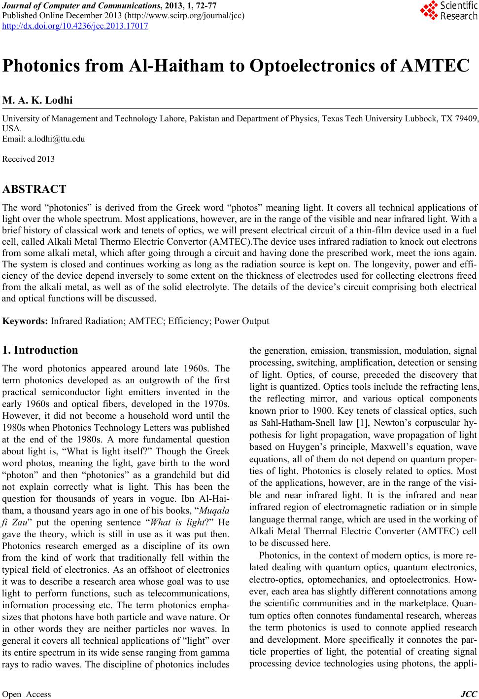
ever, achieved until today is still below the expected po-
tential of AMTEC. During an extended testing of an
AMTEC model the maximum power of its output was
observed (Figure 1) to be decreasing from 2.49 W to
1.27 W over a period of 18,000 hours of operation [7].
The degradation is primarily due to its solid electrolyte,
called bête alumina solid electrolyte (BASE). The role of
electrodes is insignificantly small compared to BASE
[8].
Before we discuss their respective contributions to the
power out and efficiency it may be in order to give a
brief description and working princ iple of AMTEC. Th is
is mostly borrowed from an encyclopedic article of the
author [9].
2. Physical Description of AMTEC
Initially AMTEC was developed as liquid-anode cycle
but soon the vapor-anode cycle system took over. The
use of the vapor-fed AMTEC cycle system has presently
been in the vogue and being investigated. A typical AM-
TEC unit is sealed, housed in a sealed container. The
working fluid should be so selected that it should have a
high negative potential, lightweight and abundantly avail-
able for cost effectiveness. An alkali metal with relative-
ly low melting point would satisfy these qualities. Out of
number of possible samples sodium (Na) is chosen for
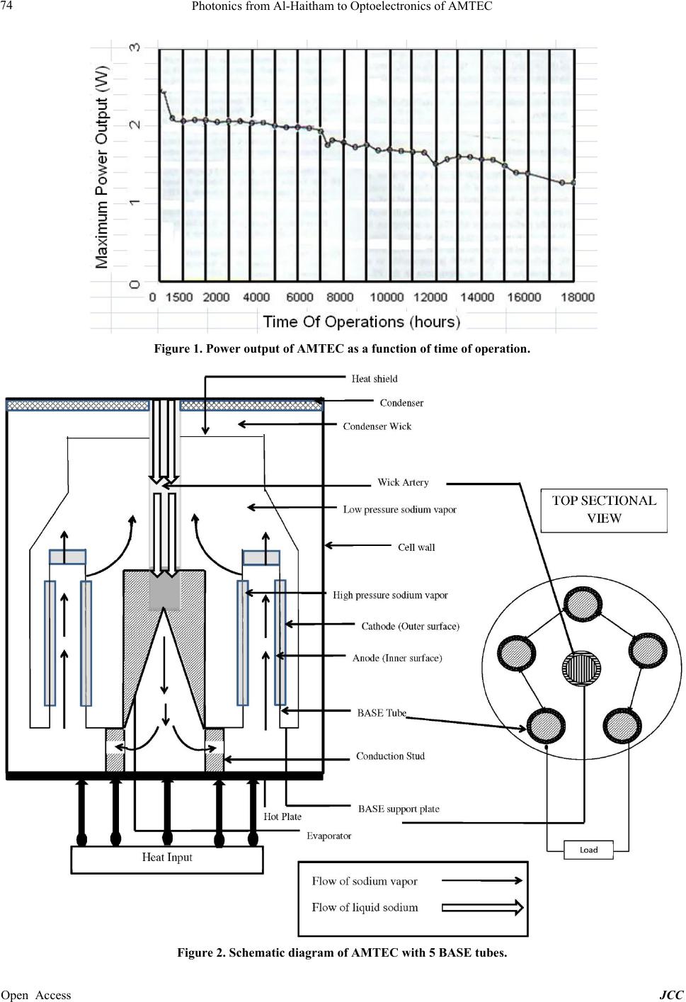
this task. At the heart of AMTEC lies a solid electrolyte
made of a dense micro-crystalline sintered ceramic ma-
terial beta” aluminum solid electrolyte (BASE)
(Na5/3Li1/3Al32/3O17) in the form of individual tubes con-
nected in series as shown in Figure 2.
The BASE separates two regions of alkali (sodium in
this case) vapor introduced; a high-temperature (900 K –
1300 K) high-pressure (20 - 100 kPa) region and a low-
temperature (400 - 700 K), low-pressure (<100 Pa) re-
gion, see Figure 2. From the physical dimensions of this
type of AMTEC cell it looks about a D-size dry cell.
Two thin, porous electrodes are placed on inside and
outside walls of the BASE, as shown schematically in
Figure 3.
The electrode mounted on the inner side of the BASE
acts as anode and the one on the outer side of the BASE
is treated as cathode. The inner and outer electrodes are
Photonics from Al-Haitham to Optoelectronics of AMTEC
Open Access JCC
74
Figure 1. Power output of AMTEC as a function of time of operation.
Figure 2. Schematic diagram of AMTEC with 5 BASE tubes.
Photonics from Al-Haitham to Optoelectronics of AMTEC
Open Access JCC
75
Figure 3. Relative positions of BASE, anode and cathode of AMTEC.
each connected with current collectors. One of the col-
lectors collects electrons at the anode (high pressure side
of BASE) and conducts them through an external load.
Electrons from the external load are brought back to the
cell at the cathode (low pressure side of the BAS E) for
the recombination with sodium ions. The requisite leads
connecting the two electrodes carry the electric current
through the load. The w orking fluid, initially in the liquid
state stored in the condenser at one of the ends of the cell,
is carried by a capillary tube, called sodium return artery
into the evaporator placed at the other end of the cell,
where it is heated and turned into vapor, see in Figure 2.
The evaporator thus maintains liquid-vapor interface
during the operatio n of the cell. The evaporator side end
carries a hot plate, which is heated from the external
infrared source. The far end of the cell, wher e the con-
denser is housed releases the heat of sodium condensa-
tion. The cell contains a radiation shield, laid against the
cell walls above the BASE tubes to reduce the parasitic
energy losses through the cell walls. In addition to radia-
tion shield a chevron radiation shield system consisting
of a requisite number of chevrons at desired angles is
placed above the BASE tubes when needed for max-
imizing the power output and efficiency. The cell is op-
erated in the vacuum.
3. Working Principle of AM TEC
On applying the infrared radiation or/and any source of
heat at one end of the cell, where the inner container is
mounted, produces the electric current at the other end of
the cell. The sodium vapor pressure at the anode/BASE
interface (the high-pressure side) is equal to the satura-
tion pressure at the evaporator (where liquid sodium is
converted into vapor) temperature. The pressure diffe-
rential between the two sides of the BASE is associated
with potential energy, which can be converted to useful
work through sodium. As the liquid sodium at condenser
temperature enters the evaporator in the hot region of the
cell, it starts absorbing the externally supplied heat until
it vaporizes and reaches the desired temperature of the
inside BASE tube. The inside BASE tube temperature is
kept slightly higher than that of the evaporator to prevent
condensation of sodium in the anode cavity and the po-
tential electric shorting of the cell. As a result of the high
pressure, sodium vapor tries to expand . The β”-alumina
is impermeable to neutral atoms and negative charges.
Thus, the only way for the pressure to be released, in
other words, for the vapor to expand, is for neutral so-
dium atoms to ionize allowing the sodium ions to pass
through the BASE wall. The sodium atoms, hence, ionize
producing sodium ions and free electrons. Due to the
thermodynamic pressure across the BASE ionization of
sodium metal vapor occurs in the hot region at the inter-
face of anode and the BASE with the following electro-
chemical reaction:
Na (vapor) + hf e + Na+
Photonics from Al-Haitham to Optoelectronics of AMTEC
Open Access JCC
76
Here h is plank constant and f is the frequency of
infrared radiation. The BASE permits the sodium ions to
pass through its material and the pressure differential
causes the movement of the ions. The positive sodium
ions accumulate on the low-pressure side. The electrons
collect on the current collector at the high-pressure side
resulting in an electrical potential, which balances the
pressure differential and prevents further flow of sodium
ions. With appropriate electrodes, this electrical potential
can be utilized to drive an electrical current when a load
is placed on the system (i.e. connecting the inner and
outer electrodes with a light bulb, CD player, or deep
space probe for example). The electrons flow from the
anode through the lead and the external load, to the ca-
thode on the outer (low pressure) side of the BASE. So-
dium ions that have passed through the BASE reach the
interface between the BASE and the cathode where they
recombine with the electrons to form neutral sodium
atoms again as they were to begin with. At the interface
of the cathode and the BASE the following reaction takes
place:
e + Na+ Na (vapor) + hf
The neutral sodium atoms escape from the interface of
the BASE and the cathode in the form of sodium vapor at
low pressure in the outer low-temperature low-pressure
region. The low-pressure sodium vapor goes to the con-
denser where it releases its energy in condensation and
condenses to the liquid state. Nearly entire temperature
drop occurs in the low-pressure vapor state. After con-
densation the condensed liquid sodium goes to the wick
annulus to the inlet of a dc electromagnetic pump or a
porous capillary wick. This system is used to return the
liquid sodium to the evaporator in the high-pressure re-
gion where it is converted to high-pressure vapor. This
way the sodium continues to recycle and maintains the
cell operation. A typical cell contains approximately 3
grams of sodium circulating through the loop at a rate up
to 0.3 grams p er minute.
The overall working of AMTEC is based on four prin-
ciples dealing with 1) thermal, 2) vapor pressure loss, 3)
electrochemical and 4) electrical models. These prin-
ciples or models and their functions could not be de-
scribed in detail in the space provided here. That d es cr ip-
tion involves lo t of mathematical derivations and expres-
sions. It should be borne in mind that the aforementioned
principles do not work independently of each other. In-
stead, they are clos e ly coupled to each other. A method is
therefore, developed to ensure a good coupling to each
other, thus allowing minimum losses over all and pro-
viding a good efficiency of the cell. It has been well
known that the AMTEC performance mainly depends on
BASE and to some extent on electrodes [8]. One of the
parameters affecting the AMTEC efficiency is the thick-
ness of BASE and electrodes. With the nanoscale modern
technology available [10,11] we have examined the in-
fluence of the variation in thickness of BASE and elec-
trodes.
4. Results of AMTEC Improvement with
Nano Scale of Electrodes and BASE
We have studied the optimization of power and efficien-
cy of AMTECT by varying the thickness of its electrodes
and BASE. The original dimension of thickness of elec-
trodes and BASE on which the analysis has been per-
formed are respectively 5.0 × 10⁷ m and 5.08 × 10³ m.
The optimum thickness of the electrode has been found
to be 1.115 × 10⁷ m with the improvement in efficiency
of 1.06%. Th is is not much of the improvement of course.
However, when the thickness of the BASE was opti-
mized and reduced to 1 × 10⁴ m the eff iciency im-
provement has been obtained by 28%, see Table 1. The
optimization of power output for the same set of thick-
ness parameters was then performed, similar results were
obtained. With the electrode optimization only the im-
provement was 0.6% but with the optimization of the
thickness of the BASE the improvement in the power
was found to be 14.8 % see Table 2.
Table 1. Efficiency optimization for electrode and BASE thickness at various temperatures.
Thickness of BASE Tube Thickness of Electrode 1023 K % Change 1123 K % Change 1173 K % Change
0.508D-3 5.0D-6 5.898855
8.116319
9.115548
0.508D-3 1.115D-7 5.951673 0.90 8.199821 1.029 9.212263 1.061
1.0D-4 1.115D-7 7.324257 23.27 10.35095 26.504 11.76178 27.969
Table 2. Power optimization for electrode and BASE thickness at various temperatures.
Thickness of BASE Tube Thickness of Electrode 1023 K % Change 1123 K % Change 1173 K % Change
0.508D-3 5.0D-6 1.386651
2.583163
3.300124
0.508D-3 1.115D-7 1.403511 0.286% 2.620202 0.456% 3.350441 0.552%
1.0D-4 1.115D-7 1.841393 7.423% 3.598503 12.054% 4.697319 14.776%
Photonics from Al-Haitham to Optoelectronics of AMTEC
Open Access JCC
77
5. Summary and Concluding Remarks
A brief history of photonics and optoelectronics with
their implication has been presented. The role of infrared
part of electromagnetic radiation has been studied with
respect to powe r generation by AMTEC. The optimum
efficiency of the device has been analyzed with an im-
provement of 28% if the thickness of the BASE is re-
duced by half a millimeter and that of the electrodes is
reduced to 111.5 nm from 500.0 nm. With the same set
of thickness parameters of electrodes and the BASE the
improvement in power was found to be 14.8 %. The effi-
ciency and power production are temperature dependent,
see Tables 1 and 2. These values were obtained by oper-
ating AMTEC at a temperature of 1173 K. The change in
electrode thickness improves the performance somewhat
insignificantly. The variation in the BASE thickness, how-
ever, makes the improvement significantly high. This
supports the previously established role of the BASE
with respect to the AMTEC p erfor mance that its degra-
dation or improvement depends primarily on the BASE.
REFERENCES
[1] R. Rashed, “A Pioneer in Anticlastic: Ibn Sahl on Burn-
ing Mirrors and Lenses,” Isis, Vol. 81, 1990, pp. 464-491.
http://dx.doi.org/10.1086/355456
[2] J. Tournier, et al., “An Analytical Model for Liquid-
Anode and Va p or-Anode Converters,” STAIF Proceeding,
AIP, 1997, pp. 1543-1552.
[3] R. Mital, et al., “Performance Evaluation of Gas Fired
AMTEC Power Sys tem,” Advanced Modular Power Sys-
tem, USA, 1998, pp. 1-2.
[4] M. A. K. Lodhi, M. Schuller and P. Housgen, “Mathema-
tical Modeling for Thermionic-AMTEC Cascade System,
STAIF Proceedings, AIP, 1996, pp. 1285-1290.
[5] M. A. K. Lodhi and V. R. Malka, “Optimization of the
TIEC/AMTEC Cascade Cell for High Efficiency,Jour-
nal of Power Sources, Vol. 96, 2001, pp. 586-691.
[6] M. A. K. Lodhi and A. Mustafa,Use of Waste Heat of
TIEC as the Power Source of AMTEC,” Journal of Pow-
er Sources, Vol. 158, 2006, pp. 740-746.
http://dx.doi.org/10.1016/j.jpowsour.2005.08.057
[7] J. Merril, Private Communication.
[8] M. A. K. Lodhi, P. Vijayaraghavan and A. Daloglu,
Time-Dependent BASE Performance and Power Degra-
dation in AMTEC, Journal of Power Sources, Vol. 93,
2001, pp. 41-49
http://dx.doi.org/10.1016/S0378-7753(00)00537-1
[9] M. A. K. Lodhi, “Alkali Metal Thermal to Electric Ener-
gy Convertor,” Encyclopedia of Electrochemical Power
Sources, Vol. 4, 2009, pp. 334-346.
http://dx.doi.org/10.1016/B978-044452745-5.00910-2
[10] M. Iqbal, M. A. K. Lodhi, Z. Majeed and D. Batani,
“Electrostatic Focusing of Directly Heated Linear Fila-
ment Gun Using EGUN,” Nucl. Instruments and Methods
in Physics Research A, Vol. 644, 2011, pp. 1-4.
[11] M. Iqbal, A. Wasy, D. Batani, H. Rashid and M. A. K.
Lodhi, “Design Modification in Rotor Blade of Turbo
Molecular Pump,” Instruments and Methods in Physics
Research A, Vol. 678, 2012, pp. 88-90.
http://dx.doi.org/10.1016/j.nima.2012.02.030