 Journal of Modern Physics, 2013, 4, 1-26 Published Online November 2013 (http://www.scirp.org/journal/jmp) http://dx.doi.org/10.4236/jmp.2013.411A2001 Open Access JMP Ab Initio Molecular Orbital Calculation for Optical and Electronic Properties Evaluation of Small and Medium Size Silicon Nano-Clusters Found in Silicon Rich Oxide Films Néstor David Espinosa Torres1*, José Francisco Javier Flores Gracia1, José Alberto Luna López1, Juan Carlos Ramírez García2, Alfredo Morales Sánchez3, José Luis Sosa Sánchez1, David Hernández de la Luz1, Francisco Morales Morales1 1Research Center for Semiconductor Devices, CIDS-ICUAP-BUAP, Puebla, México 2The Faculty of Chemical Sciences, BUAP, Puebla, México 3Research Center for Advanced Materials S.C. Unit Monterrey-PIIT, Apodaca, México Email: *siox130@gmail.com Received August 2, 2013; revised September 5, 2013; accepted October 3, 2013 Copyright © 2013 Néstor David Espinosa Torres et al. This is an open access article distributed under the Creative Commons Attribution License, which permits unrestricted use, distribution, and reproduction in any medium, provided the original work is properly cited. ABSTRACT In systems in atomic and nano scales such as clusters or agglomerates constituted of particles from a few to less than one hundred of atoms, quantum confinement effects are very important. Their optical and electronic properties are often dependent on the size of the systems and the way in which the atoms in these clusters are bonded. Generally, these nano-structures display optical and electronic properties significantly different of those found in corresponding bulk materials. Silicon agglomerates found in Silicon Rich Oxide (SRO) films have optical properties, which have reported as depended directly on nano-crystal size. Furthermore, the room temperature photoluminescence (PL) of Silicon Rich Oxides (SRO) has repeatedly generated a huge interest due to their possible applications in optoelectronic devices. However, a plausible emission mechanism has not yet widespread acceptance of the scientific community. In this re- search, we employed the Density Functional Theory with a functional B3LYP and a basis set 6 - 31G* to calculate the optical and electronic properties of small (six to ten silicon atoms) and medium size clusters of silicon (constituted of eleven to fourteen silicon atoms). With the theoretical calculation of the structural and optical properties of silicon clus- ters, it is possible to evaluate the contribution of silicon agglomerates in the luminescent emission mechanism experi- mentally found in thin SRO films. Keywords: Nano-Crystals; Silicon Clusters; Silicon-Rich Oxide; Luminescence; Magic-Number 1. Introduction Canham [1] reported visible light emission from porous silicon at room temperature in 1990 and since then, sili- con associated materials have received a huge interest and have been studied intensively for their relevance to the development of nano-electronics. In that sense, a ma- terial which has generated great interest is SRO thin film (Silicon Rich Oxide); this material exhibits optical prop- erties in the same manner to porous silicon but is signifi- cantly less assailable. Si nanocrystals (Si-nCs) embedded in dielectric ma- trices such as silicon dioxide exhibit unique optical and electrical properties which are determined by quantum size and Coulomb blockade effects [2]. Si-nCs can emit and absorb light at energies which can be controlled by their sizes. This fundamental property of Si-nCs is very useful in 3rd generation solar cells [3]. Commonly, SRO is considered as a multi-phase mate- rial constituted of a mixture of silica (SiO2), off- stoichiometric oxides (SiOx, x < 2) and elemental silicon. After thermal treatment at temperatures above 1000˚C, the off-stoichiometric oxides, SiOx (x < 2), react to pro- duce silicon nano-clusters, structures with different oxi- dation states with or without defects and silica [4]. Sili- con nano-crystals (Si-nCs) and silicon agglomerates have been characterized in SRO films employing Transmis- *Corresponding author.  N. D. E. TORRES ET AL. 2 sion Electron Microscopy (TEM) and Atomic Force Mi- croscopy (AFM). The formation and the size of Si-nCs depend on the excess silicon and annealing parameters (time and temperature) and surely of type of carried gas used. When the number of valence electrons in the clus- ters is 8, 20, 40, or 58 etc., it is well known that silicon clusters are “magic-number” [5]. The “magic-number” behavior of small size silicon clusters is frequently cor- related with the trend of binding energy per atom as a function of cluster size [6]. The electronic configuration of an atom and the number of atoms in the cluster are two factors that play the major role in the cluster stability [7]. Over the past twenty years, medium-sized silicon clusters Sin (n > 10) have attracted much attention both experimentally [8] and theoretically [9]. Considerable effort has been devoted to determine the ground-state geometric structures, namely, the global minima as a function of the cluster size n. For n ≤ 7, the global minima are firmly established by both ab initio calculations and Raman/infrared spectroscopy measurements; whereas for n ≤ 12 the global minima based on ab initio calculations [10-15] are well accepted. For 13 ≤ n ≤ 20, unbiased search for the global minima has been undertaken based on either the genetic algorithm coupled with semi-empirical tight-binding (TB) technique [16,17], or the single-parent evolution algorithm coupled with density-functional (DF) TB and density-functional theory (DFT) methods [18,19]. Set correctly the geometry corresponding to the global minimum energy is critical for a further evaluation, so reliable, of optical and structural properties, and thereby contribute properly to the under- standing of the underlying mechanisms of luminescence. Crystalline silicon has an indirect band gap, which means, every optical transition must be accompanied by the creation or annihilation of a phonon. Another disad- vantage is due to the low band gap value Eg,c-Si = 1.12 eV (at Room Temperature) corresponding to a wavelength λg,c-Si = 1107 nm: the radiation emitted by a light emitting diode (LED) built of c-Si corresponds with infrared and then is non-visible by the human eye. By usage of nano-scaled silicon structures the last mentioned disadvantage can be overcome. There are op- tical transitions in quantum confined states of Si nano- structures, which generate visible radiation. But the dis- advantage of the indirect band gap still remains. Average PL decay times for Si-nCs with diameters d ~ 3.4 nm are reported to be τPL~(100 - 500) μs at RT [20] The most intense light emission observed in SRO films obtained by LPCVD technique has been reported in films with approximately 5% excess silicon, but silicon nanocrystals were not observed in those films [21]. It is possible that silicon small size agglomerates (Sin, n < 20) were presented in these particular films (R0 = 30) which would hardly be detected due to atomic instead nano scale. Size regimes in the evolution of semiconductor spectroscopic properties were introduced by Efros [22]. Semiconductors sizes can be labeled with increasing size as molecular (n < 50 atoms), quantum dot (50 ≤ n ≤ 105 atoms), polariton (105 ≤ n ≤ 109 atoms), and finally (n > 109 atoms) for bulk semiconductor species. In this work, we calculated theoretically the IR, UV- Vis and Raman spectra and a selected set of properties of small and medium size silicon agglomerates (agglomer- ates size less than 1.5 nm). The equilibrium energy cal- culated of several propose d Si clusters at ground state and the six first excitation states calculated result very useful to evaluate the possible contribution to the PL from different silicon structures present in SRO films. 2. Theory of Electronic States in Nanocrystals The excitation of nanocrystals with photons can only happen from electronic states in the valence band to electronic states in the conduction band. To obtain the electronic states in a nano-crystal the assumption that nanocrystals have a spherical shape is used. S. V. Gapo- nenko [23] used spherical coordinates r, θ and ϕ and the Hamiltonian: () 2 2 2 Ur m =−∇ + (1) where U(r) is the total potential energy of the electron inside the quantum dot. In this Hamiltonian the Laplace operator in spherical coordinates must be used: () 2 2 2 22 22 2 11 sin sin sin 2 Hr rr mr Ur mr θ θθθ θ φ ∂∂ =− ∂∂ ∂∂ ∂ −+ ∂∂ ∂ + (2) Due to the spherical symmetry of the potential a sepa- ration of the wave function leads to the following wave function: ()() () , ,, ,, , nl nlmlm ur rY r θ θ = where ( , lm Y θ ) is the spherical functions, n is the prin- cipal quantum numbers, l is the orbital number and m the magnetic number. The angular momentum L is deter- mined by the orbital number l: () 210,1,2,,Lll ln=−=1− (4) The component parallel to the z axis is determined by the magnetic quantum number m:1 1 () ()() sin 1 †Bessel function:l jl l ξξ ξξ ξ ∂ =− ∂ Open Access JMP  N. D. E. TORRES ET AL. 3 ,1,2,,1, z mml llll==−−+−+− (5) Inserting into the Schrödinger equation must satisfy the equation: () ,nl ur () () 22 2 22 d1 2d2 uUrllu Eu mrmr −++ += (6) In order to obtain a solution to this equation the poten- tial is approximated as infinitely high which leads to the following expression for the energy values of the elec- tronic states in a spherical nano-crystal: 22 2 2 nl nl Ema = (7) where χnl are the roots of the spherical Bessel functions†. In the real space the electron and the hole are interact- ing via coulomb attraction. This bound pair of electron and hole is known as excitons. Quantum confinement occurs if the Bohr radius, of the excitons is larger than the size of the nano-crystal. Due to the high potential of the silicon dioxide (approximately 9 eV) which surrounds the silicon nanocrystals the excitons are confined within the volume of the nano-crystal. This leads to further changes of the band structure and the emissions spectrum. Starting from the energy value already calculated and applying perturbation theory it is possible to obtain a correction factor due to the effective mass of the electron and hole respectively. ( nl E ) Additionally, the Coulomb interaction between the electron and the hole has to be considered. A combination of both approaches leads to the Hamiltonian in the lowest excited state: 22 22 olarization terms 2 eh ehe h e Hrrm m ∇∇ =−−+ + − (8) With the distance of electron and hole re − rh, their ef- fective masses me and mh respectively and the dielectrical constant . We assume in Equation (1) that the total potential en- ergy U(r) to be of the following form: ()() () osp UrU rVr=+ (9) The second part Vsp(r) describes an interaction between the electron and its image, arising due to the charge po- larization on the boundary between the silicon nano- crystal and its dielectric surrounding. Vsp(r) is often re- ferred to as a self-polarization term. It can be represented as: () () () 22 2 0 1 21 l sd sp l l ssd el Vr Rll R εε εεε ∞ = −+ =++ r (10) where ε and d are the static dielectric constants of silicon and the dielectric matrix, respectively. The po- larization terms enter because we must consider the cor- rect form of the Coulomb interaction in the presence of the crystallite surface. An analytical approximation for the lowest eigenvalue (i.e., the first excited electronic state) is: ε 222 2 1.8 smaller terms 2 eh G eh mm e EE Rmm R + π ≅− ++ (11) where EG is the bulk band gap, R is the size of the nano- crystal, the term ∝ to R−1 is the coulomb term and the term ∝ to R−2 is the shift as a result of quantum localization of electrons and holes (quantum confinement). This simple formula is possible because the correlation between elec- tron and hole positions, induced by the Coulomb interact- tion, is not strong. The major effect is additive, inde- pendent confinement energies for electron and hole. Latest energy equation connects in a very simple way the emitted wavelength of a nano-crystal to its size, by means of: [] 1239.7 nm G Eh νλ =≈ (12) In 1984 Brus [24] suggested the first theoretical calcu- lation for semiconductor nanoparticles based on “effective mass approximation” (EMA). This approximation as- sumed that an exciton is confined to a spherical volume of the crystallite and the mass of electron and hole is sup- planted with effective masses ( and ) to define the wave function. * e m* h m ** 22 2** 0 1.786 84 eh g bulk eh r mm he EE RmmR εε + =+ − π 2 (13) 0 is the permittivity of vacuum and r is the relative permittivity. Four year later, in 1988 Kayanuma [ ε ε 25] accounted for the electron-hole spatial correlation effect and modified the Brus Equation, including a taking away term proportional to Rydberg energy. 3. Analysis and Discussion of the Results Obtained For many years, different methods have been used for preparation of silicon nano-crystals, for instance, chemi- cal vapor deposition [26], Si ion implantation [27], col- loidal synthesis [28], magnetron sputtering [26], and electron beam evaporation [29]. A high-temperature thermal treatment at temperatures above 1000˚C is gen- erally required in order to produce the crystallites. All these techniques allow one to form silicon nCs with sizes mainly ranging from 2 - 6 nm, and it is possible obtain silicon nCs with sizes less than 2 nm in SRO films as de- posited with Ro = 30 prepared using LPCVD technique. Their electronic and optical properties depend on the preparation conditions and method of fabrication. How- ever, there are some common properties typical for silicon Open Access JMP 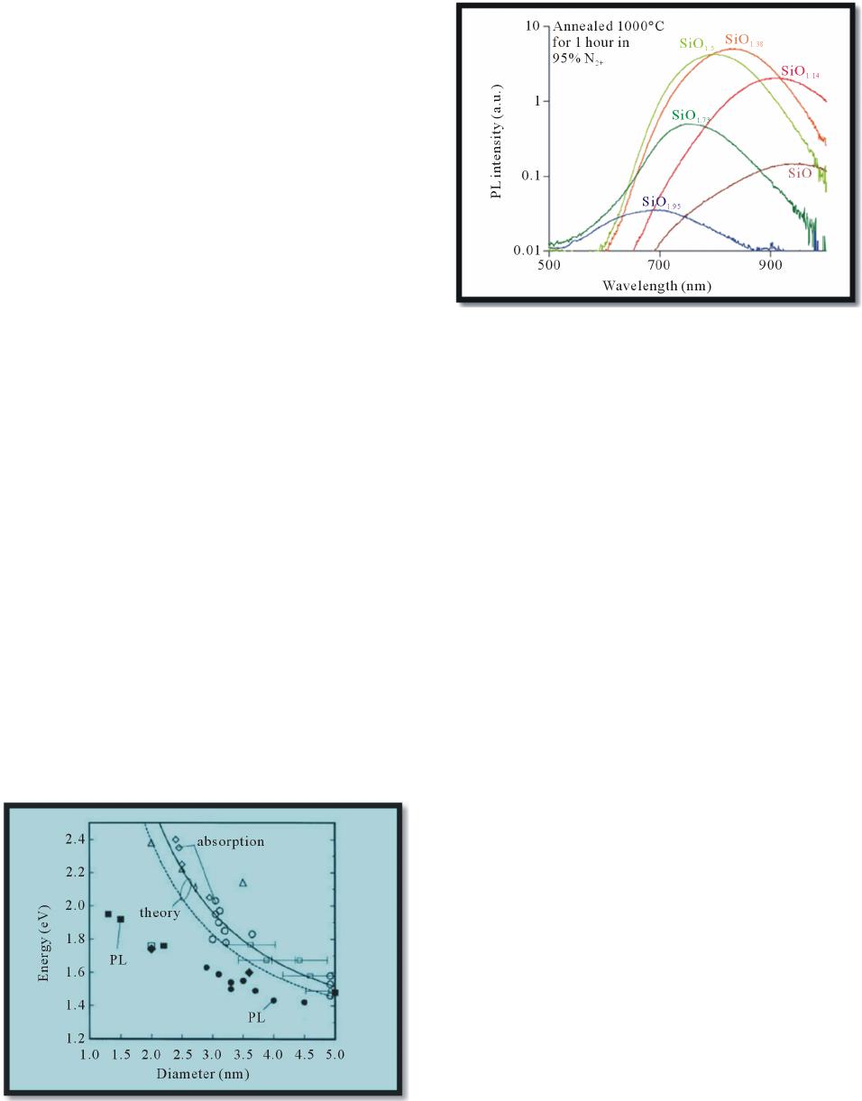 N. D. E. TORRES ET AL. 4 nCs, independent of the fabrication technique employed. In particular, the nanocrystals’ surroundings, either vac- uum or some host material like SRO, represent a high potential barrier for carriers of both kinds. Such a barrier is often referred to as a confining potential that mainly defines the energy spectrum of the nano-crystal. Figure 1 displays the optical band gap of silicon nanocrystals obtained from optical absorption (unfilled symbols) and PL data (filled symbols). Dashed and con- tinuous lines are calculated values with and without ex- citonic correction, respectively. Silicon nCs are capable of emitting electromagnetic energy in the visible spectrum. This is in contrast with bulk silicon, in which energy of the interband transition corresponds to the silicon band gap energy of 1.12 eV. The variation of the photon frequency in nanocrystals compared to the bulk material is a universal phenomenon taking place in huge of semiconductor materials. The energy of the emitted photon increases as the nano-crystal size decreases. Such an increase is usually called a “blue- shift” because the photon energy shifts toward the shorter- wavelength side of the visible spectrum. This blue-shift is illustrated for Si nCs in Figure 2. Here, the mean nC size is controlled via the silicon excess concentration, with the smallest nCs occurring in the most silicon deficient samples. Reduction in intensity on the silicon-poor side of the compositional map is due to the lower number density of nCs, and on the silicon-rich side it is due to the opening of non-radiative pathways in large and highly interconnected nano-clusters. There is a legitimately large uncertainly in the calcu- lated values of the optical gaps as a function of nCs di- ameter. Doubtless, several factors influencing the accu- racy of the optical-gap measurements are as follows. First, the nanocrystals studied by different research groups have been prepared using different techniques. As a result, the Figure 1. Optical band gap of silicon nano clusters. Theo- retical calculus vs experimental data compilated by Delerue [31]. Figure 2. PL spectra of silicon nCs in SiO2. The 200-nm- thick samples were approximately identical except for the amount of excess silicon [32]. nCs have different surroundings, surface bonds, and shapes, all of which could lead to scatter in the experi- mental data. Second, it is difficult to determine exactly the dot sizes and the size distribution in luminescent ag- glomerate of nCs. Finally, using the mean size in a cluster of nCs in a plot like Figure 1 can be confusing, since it is possible that the observed PL peak does not correspond exactly to the mean size but instead to the largest PL rate. Theoretically, the problem persists mainly due to the difficulty to define an appropriate parameter for deter- mining the diameter (equivalent). By simplicity a sphere is used in most of the models suggested, since the actual shape of the agglomerates formed is totally irregular. Figure 3 shows the calculated Van Der Waal surfaces for isomers Si7. In this case, only the isomer with lowest energy is acceptably symmetric. And even then it is dif- ficult to choose the appropriate size. Thus, for example the greatest distance found in isomer 7A is which can be measured from either silicon atoms placed in the vertex of a pentagon to its second nearest neighbor obtaining values in range of 4.050 to 4.053 Å for Si-Si not bonded in ten possible measures; of 2.506 to 2.508 Å in five measures corresponding to silicon atoms contiguous around the pentagon (bond distance), the dis- tance between silicon atoms in two pyramid corners or vertex is 2.568 Å and the distance between a silicon atom in pentagon to the silicon atom in pyramid corner is 2.486 to 2.488 Å (ten bond distance values). Assuming for silicon a Van der Waals radii of 2.1 Å, then the diameter for Si7 isomer 7A could be in range 0.4586 to 0.6153 nm. So, how can we set the most ap- propriate diameter or crystallite size? For solve this, we employ a space-filling model, also known as a calotte model or CPK models, is a type of three-dimensional molecular model where the atoms are represented by spheres whose radii are proportional to the Open Access JMP  N. D. E. TORRES ET AL. Open Access JMP 5 energy reported by Raghavachari and Rohlfing [6] No qualitative change in the geometry of these isomers was found except the capped trigonal prism. The lowest-en- ergy isomer of Si7 corresponds with structure 7A, a pen- tagonal bipyrimid with D5h symmetry, in accordance with the experiment [34] and previous theoretical studies [6]. Note that the structures of small silicon clusters are dif- ferent from the tetrahedral coordination characteristic of bulk silicon. Table 2 contains specific bonds calculated information for Si7 structures. Table 1 displays calculated structural and geometric properties for Si7 nano-cluster. The most stable structure (7A) presents the lowest Dipole, CPK Area (Å2) CPK volume (Å3), ovality and polariza- bility parameters and the highest symmetry and band gap. Figure 6 shows ovality and polarizability calculated pa- rameter for Si7 isomers. Ovality is a measure of how the shape of the molecule approaches a sphere or cigar. Ovality is described by the ratio of volume and area. radii of the atoms and whose center-to-center distances are proportional to the distances between the atomic nuclei, all in the same scale. CPK models are distinguished from other 3D representations, such as the ball-and-stick and skeletal models, by the use of “full size” balls for the atoms. They are useful for visualizing the effective shape and relative dimensions of the molecule, in particular the region of space occupied by it. Table 1 displays values for CPK volume and CPK area for isomers Si7. For isomer 7A, using CPK volume we obtain d1 = 6.987 Å (≈0.7 nm) and d2 = 7.400 Å (≈0.74 nm) when we use CPK area. Finally, we can co-relate CPK area and CPK volume, obtaining the diameter [Å] with equation: 3 volume 2 AREA 4 6 6CPK 32 CPK 42 D D D ×π × = π = (14) Substitution of values gives D = 6.2295 Å, for isomer 7A. 7A 7B 7D 7C Figure 4(a) corresponds with AFM image 3D. Adjunct to coordinates (0, 3.5) it is possible to find thickness less than 5 nm [33]. Whereas in Figure 4(b) adjacent to co- ordinates (0, 2.8) it is possible to find thickness less than 1 nm. In Figure 5(a) we can appreciate roughness less than 1 nm for SRO films as deposited with a Ro = 20 and less than 5 nm for films deposited with Ro = 10 and Ro = 30. Whereas Figure 5(b) is a 2D AFM image for SRO film deposited by LPCVD, in blue line (Ro = 30) we are able to find height less than 1 nm. For Ro = 20 (red line) is pos- sible observe height less than 1 nm around χ ≈ 1.2 μm. Finally, for Ro = 10 (black line) there is a small region with altitudes less than1 nm everywhere χ ≈ 1.95 μm. The highest agglomerates found correspond to Ro = 10 and it is approximately 25 nm. 3.1. Structural and Optical Properties for N = 7 Figure 3. Calculated Van Der Waal surfaces for isomers Si7. For Si7 we have evaluated four geometric isomers of low- Table 1. Calculated Properties for Si7 nano-cluster. Isomer E (au) E LUMO (eV) E HOMO (eV) band gap eV Dipole (debye) CPK Area (Ų) CPK Volume (ų)Ovality** Nsymop polarizability* 7A -2026.40489 −3.17 −6.35 3.177114890.01 172.06 178.60 1.12184512 4 55.1102671 7B −2026.34772 −3.70 −5.60 1.897523351.12 174.00 180.46 1.12674305 1 55.5653083 7C −2026.34325 −3.25 −5.61 2.363334240.25 183.44 185.93 1.16445201 1 55.8984076 7D −2026.34330 −3.26 −5.62 2.364984710.26 183.56 185.96 1.16504567 2 55.9003733 *; ** 2 Polarizability0.08VDW _Volume13.0352hardness0.979920hardness41.3791=×− ×+×+ () () () () 23 vality43 4AV=×π×××πO; () HOMO LUMO hardness 2EE=− −. 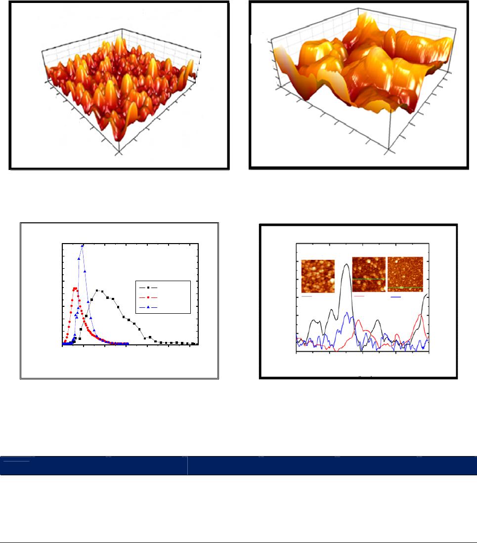 N. D. E. TORRES ET AL. 6 T d = 1005˚C 0.0 0.5 1.0 1.5 3.0 4.0 2.5 3.5 X[μm] 2.0 0.0 0.5 1.0 1.5 2.0 2.5 3.0 3.5 4.0 0.0 5.0 10.0 15.0 20.0 Z[nm] Y[μm] 0.0 0.5 1.0 1.5 3.0 4.0 2.5 3.5 2.0 0.0 0.5 1.0 1.5 2.5 3.0 3.5 4.0 0.0 20.0 Z[nm] Y[μm] 2.0 X[μm] 40.0 60.0 80.0 100.0 (a) (b) Figure 4. (a) AFM image 3D obtained of a SRO film deposited by HFCVD at 1005˚C; (b) AFM image 3D obtained of a SRO film deposited by HFCVD on silicon substrate. 0510 15 20 25 30 0 3000 6000 9000 12000 15000 18000 21000 24000 Frequency Roughness (nm) Ro = 10 Ro = 20 Ro = 30 Histogramas As-Deposited 30 25 20 15 10 5 0 0 12 3 4 X (μm) Ro=10 Ro=20 Ro=30 As-Deposited Profile Height (nm) (a) (b) Figure 5. (a) Histogram of roughness [nm] for SRO films as deposited; (b) 2D Image that shows the selection of the Rough- ness and profile characteristics for statistical analysis of SRO10, 20 and 30 As-deposited films on Silicon for a scan size of 4 × 4 μm2. Table 2. Small nanoclusters Si7 exhibit a coordination different that found in bulk silicon (tetra coordinated). Isomer Number of Silicon atoms with 2 bonds Number of Silicon atoms with 3 bonds Number of Silicon atoms with 4 bonds Number of Silicon atoms with 5 bonds Number of Silicon atoms with six bonds Total Number of Si-Si bonds 7A 5 2 15 7B 3 1 2 1 15 7C 1 3 3 15 7D 1 4 2 14 In Raman spectroscopy a vibrational mode is active due to a change in the polarizability during the vibration. On the other hand, a vibrational mode is active in FTIR as consequence of a change in the dipole moment during the vibration. For isomer most stable (7A), FTIR spectra has a peak at 406 cm−1. Due to poor symmetry or anti-symmetry of isomers 7B, 7C and 7D there is a shift in frequency vi- bration values (until 529 cm−1) and appears additional small peaks, see Figure 7. The second most intense peak in isomer 7C has a fre- quency of 436 cm−1 (indicated with a small red circle on Figure 7). Isomer 7D displays a similar peak in the fre- quency 439 cm−1. Luna et al. [33 ], have reported a peak at Open Access JMP 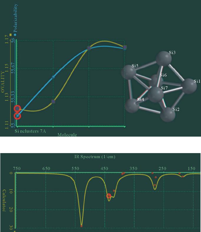 N. D. E. TORRES ET AL. 7 Figure 6. Ovality and polarizability plots for Si7 structures. Right side: Structure 7A (the lowest energy isomer). Figure 7. FTIR spectra for isomer 7C. 440 cm−1, in SRO films deposited at 873˚C by HFCVD, but they associated this vibration frequency with Si-O rocking. UV-Vis spectra calculated for isomers Si7 predict lu- minescence in visible region, except for most stable (isomer 7A) which results with emission in UV region. This fact could be associated with the similarity with tetrahedral coordination in bulk (there are five silicon atoms with four bonds each one and only two with five bonds). Figure 8 displays UV-Vis spectra for isomer 7D. In Table 3 we collect luminescence calculated data for isomers Si7. The isomer Si7 with the highest stability (7A), results with violet emission expected and other isomers with less stability display a second expected peak in IR region. 3.2. Structural and Optical Properties for N = 12 Bahel and Ramakrishna [10,11] have examined 15 iso- mers of Si12 and shown that the pentagonal and tetragonal prismatic families are higher in energy than the trigonal prismatic family. Zhu et al. [35] obtain similar conclusion after examining several new low-energy isomers. For Si12 isomers found by Zhu [35], we have re-evaluated using HF/6-31*, and we obtains some differences in results, see Table 4. Whereas Zhu et al. results indicate that isomer 12A is the lowest-energy; our results give isomer 12E as the most stable structure. Dipole moment calculated for isomers Si12 varies in range from 0.0 to 2.75 Debye’s, and band gap fluctuates from 1.558 until 2.648 eV. Table 5 contains the calculated properties for isomers Si12 organized from low to high energy. Sorted in this way, it is not possible correlate them with other parameter like dipole moment, band gap, polarizability, ovality or the size. The average size for isomers Si12, using CPK area and CPK volume models results 0.8595 nm.Optical pro- perties calculated for isomer Si12 are presented in right Open Access JMP 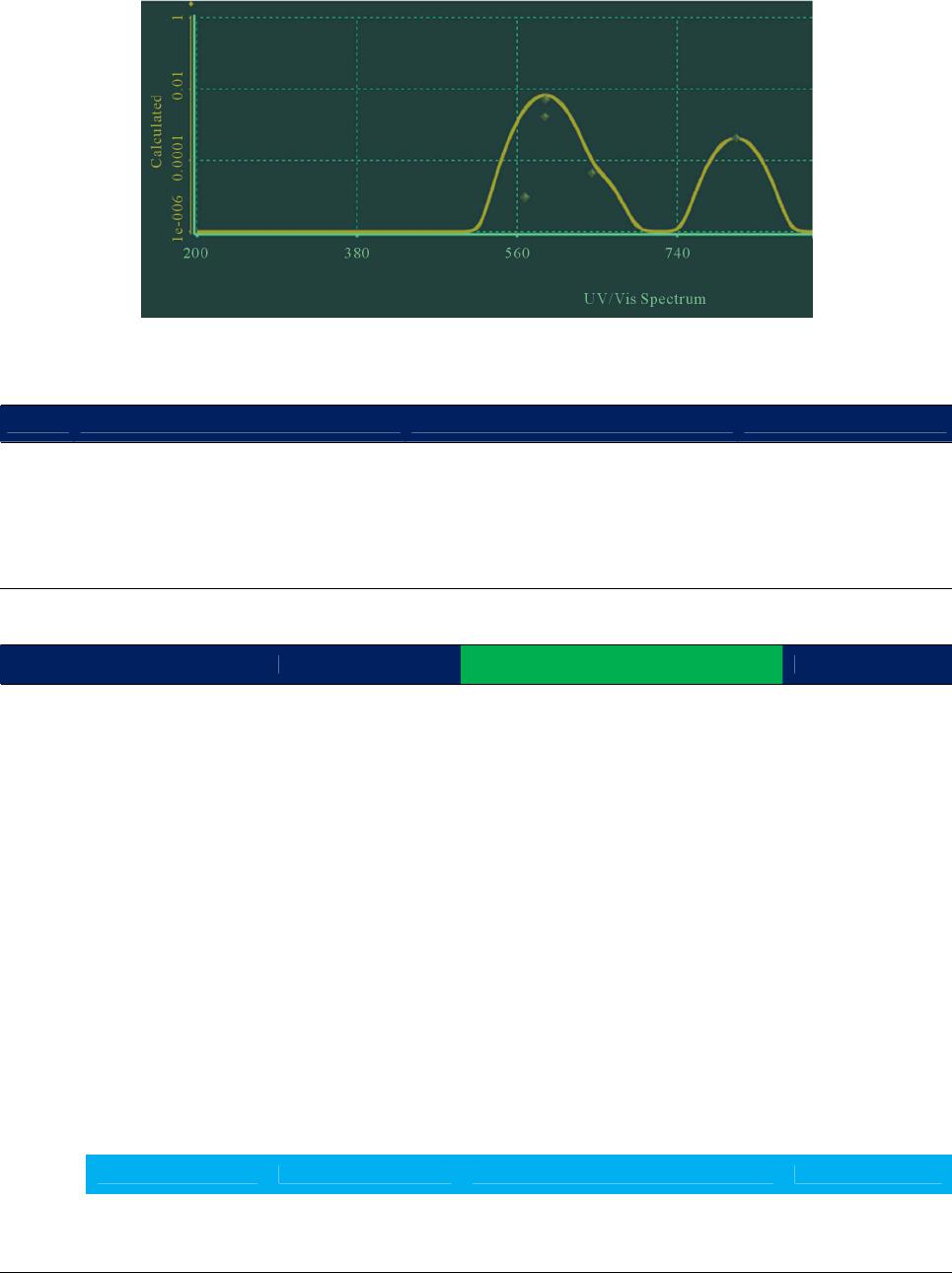 N. D. E. TORRES ET AL. 8 Figure 8. UV-Vis spectra for the isomer 7D. Table 3. Calculated luminescence peaks for the isomers Si7. Isomer The Most intense peak emission [nm] 2nd More intense peak emission [nm] 3rd peak emission [nm] 7A 382.41 (violet) 7B 660.93 (red) 930.99 (IR) 777.58 (IR) 7C 598.11 (orange) 807.37 (IR) 7D 591.98 (orange) 806.26 (IR) Table 4. Comparation of energies calculated of Si12 isomers. Isomer HF/6-31G* ref [ZZ] MP2/6-31G* ref [ZZ] OUR RESULTS USING HF/6-31G* Point Group 12a −3466.75512 −3467.97520 −3473.81817 (C2v) 12b −3466.72241 −3467.96359 −3473.84833 (Cs) 12c −3466.68583 −3467.94708 −3473.82730 (Cs) 12d −3466.72986 −3467.94023 −3473.829488 (C2v) 12e −3466.74850 −3467.93946 −3473.85018 (C1) 12f −3466.68104 −3467.92139 −3473.83045 (Cs) 12g −3466.71823 −3467.91483 −3473.82394 (Cs) 12h −3466.67983 −3467.91127 −3473.82681 (C3v) 12i −3466.56063 −3467.90996 −3473.80236 (D4h) 12j −3466.69196 −3467.90872 −3473.82995 (C2v) 12k −3466.63861 −3467.90709 −3473.81306 (C5v) 12l −3466.68552 −3467.89061 −3473.84834 (C2v) ref [32] MP3/6-31G* MP4(SDQ)/6-316* CCSD/6-31G* CCSD(T)/6-31G* 12A −3467.87303 −3467.96718 −3467.92573 −3468.03985 12B −3467.84017 −3467.94730 −3467.90060 −3468.02069 Open Access JMP  N. D. E. TORRES ET AL. 9 Table 5. Calculated properties for Si12 nano-clusters (sorted by energy value). Isomer Energy homo eV Energy Lumo eV Dipole Debye CPK Area (Ų) CPK Volume (ų) band gap eV ovality D [nm] (using CPK Area D [nm] (using CPK Volume FTIR frequency of most intense peak cm−1 UV-Vis wavelength of most intense peak [nm] 12E −5.77 −3.60 0.46 247.51 288.66 2.171419701.171786810.8876 0.8200 485 826.45 (IR) 12L −5.80 −3.88 0.70 249.32 290.45 1.926875311.175504430.8908 0.8217 415 720.43 (red) 12B −5.80 −3.88 0.70 249.26 290.36 1.924999911.175462730.8907 0.8216 415 720.22 (red) 12F −5.82 −3.17 2.75 245.18 288.52 2.648491191.161119640.8834 0.8198 435 562.76 (green) 12J −5.59 −3.79 0.31 249.86 291.95 1.801511561.174027280.8918 0.8231 442 830.71 (IR) 12C −5.69 −3.77 1.19 250.22 291.07 1.918010371.178072380.8925 0.8222 408 635.2 (red) 12H −5.78 −4.07 0.00 254.22 296.04 1.706528141.183472410.8996 0.8269 354 733.33 (red) 12G −5.43 −3.37 0.98 251.45 292.34 2.062211741.180439490.8946 0.8234 427 576.75 (yellow) 12A −5.66 −3.16 0.39 252.59 290.90 2.498778131.189702420.8967 0.8221 448 627.76 (red) 12K −5.54 −3.99 0.44 259.84 294.83 1.558762481.212942700.9094 0.8258 492 772.49 (IR) 12I −5.67 −3.51 0.01 264.24 297.70 2.160614891.225559310.9171 0.8284 445 641.76 (red) 12D Fails side of Table 5. FTIR calculated vibrations frequencies of 442, 448 and 445 cm−1 (highlight in yellow) for isomers 12J, 12A and 12I are in excellent agreement with experimental results and they were reported in SRO films deposited by HFCVD at temperatures in range of 750˚C to 873˚C). Also UV-Vis calculations are in Table 5. All Si12 iso- mers have an expected emission in visible range. We have selected the most intense peaks for each isomers and we plotted them in Figure 9. We can conclude that the likely most intense emission of isomers Si12 will be in color red. Chemical Function Descriptors CFD’s are descriptors given to a molecule in order to characterize or anticipate its chemical behavior or to identify commonality among molecules with different structures. They parallel terms in a chemist’s vocabulary such as lone pair (to suggest the role of a hydrogen-bond acceptor) and sterically crowded (to suggest that getting close may be difficult). Figure 10 displays VDW surfaces for isomers Si12 (12A, 12B, 12C and 12E) and includes sketchs 12F to12 L to represent CFD’s for isomers Si12 (12F to 12L). We can appreciate silicon atoms with coordination different respect to found in bulk. For instance, the isomer 12H has six silicon atoms with only three bonds, three silicon atoms with five bonds, two with six bond and one with seven bonds.That is, none of the twelve silicon atoms present in the isomer 12H is tetra coordinated. Figure 11 includes FTIR spectra calculated for the most stable isomer Si12. The most intense peak with a frequency of 485 cm−1, corresponds to silicon atoms vi- bration that contains only three bonds. UV-Vis spectrum for isomer 12E is shown in Figure 12. In this case, luminescence is observed in a wide interval of visible region and it extends to near IR, beginning in 574.67 nm and ending in 826.43 nm we can easily identify six emission states. 3.3. Structural and Optical Properties for Si8 Isomers In 1988 Raghavachari and Rohlfing [6] reported seven low-energy isomers Si8 on the basis of the HF/6-31G(d) level of theory. Later, Xiaolei et al. [36] in 2003 reported eight isomers Si8, after optimizing the geometry at the MP2/6-31G(d) level followed by the total-energy cal- culation at the CCSD(T)/6-31G(d) level. Among the seven isomers originally cited, six geometric isomers, have the same structure as Xiaolei [36] suggested despite of some differences in energy ordering and geometric parameters due to different levels of theory employed. We evaluated full geometry optimizations followed by the total-energy calculation at the HF/6-31G* level, for eight structures suggested by Xiaolei [36], who reported isomer 8A as the lowest energy Si8. Our results indicate that isomer 8E has the lowest energy. For isomers Si8, FTIR spectra are displayed in Figure 13. In this case, there are 18 degree freedoms and most of them correspond with frequency vibrations of very low intensity. In Table 6 we collect numerical data. For iso- mers 8C, 8G and 8B, the highest vibration intensity cor- responds with the maximum wavenumber. In right column of Table 7 we include the wavelength of the energy level with the highest emission. All results obtained predict emission in visible region for isomers Si8. A selected set of Si8 isomers UV-Vis spectra are shown in Figure 14. Figure 15 displays agglomerate’s shape and coordina- tion isomers’s Si8. We can appreciate sub-coordinated (tri) and supra-coordinated (penta and hexa) silicon atoms, Open Access JMP 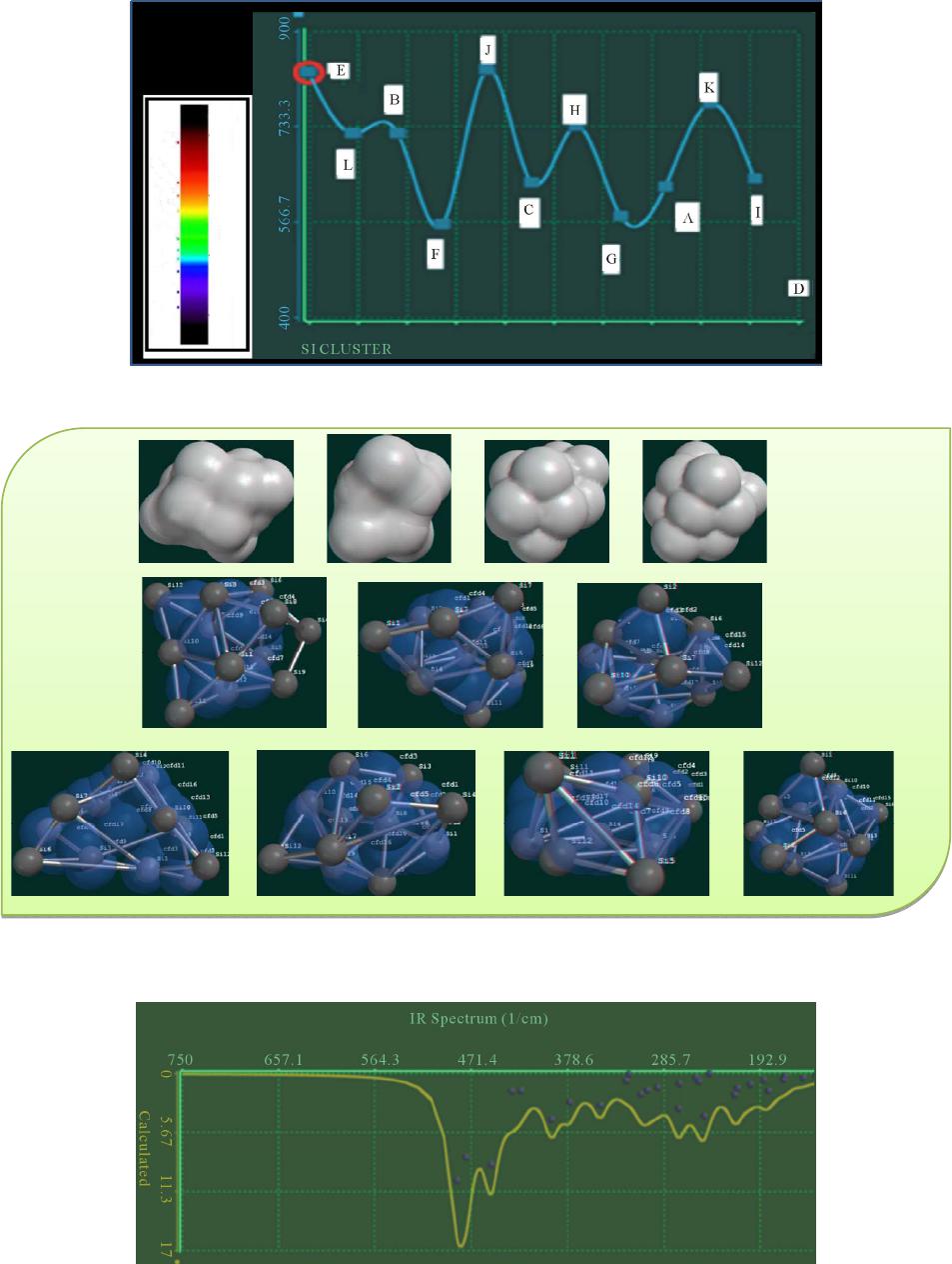 N. D. E. TORRES ET AL. 10 WAVELENGTH nm 400 500 600 700 UV IR Figure 9. Wavelengthmax for isomers Si12. 12A 12B 12C 12E 12F 12G 12H 12I 12J 12K 12L Figure 10. Sketch 12A to 12E display VDW surfaces for isomers Si12 (A, B, C and E). 12F to12L represent CFD for isomers Si12 (F to L). Figure 11. IR spectra calculated for silicon isomer with the lowest-energy 12E. Open Access JMP  N. D. E. TORRES ET AL. 11 Figure 12. Luminescence spectra calculated for silicon isomer 12E. Figure 13. FTIR calculated spectra for isomers Si8 (A to D). Open Access JMP  N. D. E. TORRES ET AL. Open Access JMP 12 Table 6. Calculated properties for isomers Si8. Isomer Energy [hartree] E HOM O [eV] E LUMO [eV] Band gap [eV] Dipole moment [debye] CPK AREA (Ų) CPK VOLUME (ų) D = NANO CRYSTAL SIZE [nm], using equation 14 Number of Si-Si bonds CAN (Equation (15)) 8A −2315.85400 −5.48 −3.81 1.66577122 0.00 190.10202.88 0.640326546 19 4.75 8B −2315.84487 −5.40 −3.90 1.49418089 0.94 189.68203.19 0.642714381 17 4.25 8C −2315.84982 −5.66 −3.40 2.25498620 0.99 190.19203.73 0.642716601 17 4.25 8D −2315.84767 −5.10 −3.33 1.76459166 0.80 193.41203.76 0.632105836 16 4.00 8E −2315.86794 −5.80 −3.21 2.58956912 0.00 191.09203.00 0.637395306 18 4.50 8F −2315.86179 −6.06 −3.86 2.19571567 0.46 191.99203.99 0.637486965 18 4.50 8G −2315.84487 −5.40 −3.90 1.49141814 0.94 189.69203.21 0.642738633 19 4.75 8H −2315.84642 −5.65 −3.57 2.07800261 0.85 192.08205.18 0.640911951 20 5.00 AVG −2315.85217 −5.57 −3.62 1.94177944 0.62 191.03203.62 0.639549527 MIN −2315.86794 −6.06 −3.90 1.49141814 0.00 189.68202.88 0.632105836 MAX −2315.84487 −5.10 −3.21 2.58956912 0.99 193.41205.18 0.642738633 St.dev 0.00853663 0.29 0.28 0.39848214 0.42 1.36 0.74 0.00372214178 Table 7. Calculated numerical data in FTIR and UV-Vis spectra for isomers Si8. Isomer Wavenumber of max vibration cm−1 Wavenumber with max Intensity cm−1 Wavelength of the highest emission nm 8E 508.432 507.490 535.14 8F 479.146 408.119 834.12* 8A 491.027 471.044 701.32 8C 470.320 470.320 510.90 8D 477.413 273.661 522.91 8H 485.637 372.866 643.56 and 662.48 8G 451.894 451.894 682.99 8B 452.367 452.367 595.57 *There are other three energy levels in isomer 8F with emissions closely respect the highest emission (593.17, 711.70 and 753.90 nm). Using this definition, we can calculate for isomer Si8 CAN values in the range of 4 to 5 (refer to Table 6) besides tetra-coordinated. In silicon bulk there is only tetra-coordinated silicon atoms. It’s possible to suggest growing mechanisms for silicon nano-crystals based on coordination number. Isomers Si8 have been cited as a magic number. The “magic-number” behavior of small silicon clusters has been correlated with the trend of binding energy per atom as a function of cluster size [6]. Luo, Zhao, and Wang [7] pointed out that two factors can play major role in the cluster stability, one is the electronic configuration of an atom and another is the number of atoms in the cluster. We define the useful relationship “Coordination Average Number (CAN)” as: The energies calculated for isomers Si8 are included in Table 6. The energy differences regarding the isomers with lowest energy are in range from 0.16746 to 0.62787 eV. Band Gap calculated varies between 1.49141814 and 2.58956912 eV. In this case, the isomer 8E shows the global minimum energy and the maximum band gap. Dipole moments are in range 0.0 to 0.99 Debye. () 2number of SiSi bonds CAN umber of Silicon Atoms ×− = (15) Statistical values for optical and geometrical parame- ters are listed in bottom of Table 6. In 1999 Luo et al. thought that isomer 8H to be the global minimum based on a semi-empirical method. The isomer 8 G, a singly- capped pentagonal bi-pyramid, was also previously thought o be the global minimum based on the tight-binding t  N. D. E. TORRES ET AL. 13 Figure 14. Calculated luminescence spectra for isomers Si8 (E to H). 8G 8 8E 8C 8B 8F 8H 8D Figure 15. Agglomerate’s shape and coordination isomers’s Si8, using ball and wire model. molecular dynamics calculation [37]. 3.4. Structural and Optical Properties for Si9 Isomers For isomers Si9, the global-minimum isomer appears to be the stacked distorted rhombi (9A) with an additional atom capped on top [38,39]. This lowest-energy structure was predicted by Vasiliev, Ogut, and Chelikowsky [40] and confirmed later by other groups [39,41]. It can be also viewed as a bi-capped pentagonal bi-pyramid. The isomer Open Access JMP  N. D. E. TORRES ET AL. 14 9B, also a bi-capped pentagonal bi-pyramid (but the two caps are on the same side of the pyramid), is a local minimum. In this case, we evaluated five isomers (9A to 9E) the first four as Xiaolei Zhu and X. C. Zeng [36] suggested, and additionally we evaluated the isomer 9E, and the results obtained indicate that the global-minimum energy isomer could be the isomer 9A with an energy almost equal than 9C (difference of −6.7*10 - 6 au), in accordance with most of results previously reported. The structures and FTIR spectra calculated for isomers Si9 are displayed on Figure 16. Spectra for isomers 9A and 9C are closely similar as expected, numerically the maximum wavenumber calculated are 480.892 and 479.594 cm−1 respectively. In a similar way, FTIR spectra for isomers 9B and 9E are comparable with the highest vibration intensity at 392.101 and 386.835 cm−1, accord- ingly. Isomer 9D displays two intense peaks, at wave- numbers of 485.265 and 450.588 cm−1. Isomers Si9 have 21 freedom degree and the number of basis functions employed was 171 in a basis set 6-31G(d). UV-Vis spectra calculated for isomers Si9 are displayed on Figure 17. Similarities discussed in FTIR spectra about isomers 9A and 9C are found again in UV-Vis spectra. Isomers Si9 show a blue-shift respect to isomer Si8, but most of them present a maximum expected emission in green. Specifically isomer 9D displays a very wide emission since green to IR. Quantitative information for isomers Si9 is collected in Table 8. We can say that isomers 9A and 9C are nearly iso-energetic, they share the global minimum (relative Figure 16. Structures and FTIR spectra calculated for isomers Si9. Open Access JMP  N. D. E. TORRES ET AL. 15 Figure 17. UV-Vis spectra calculated for isomers Si9. Table 8. Calculated properties for isomers Si9. Isomer E (au) rel. E (eV) Dipole (debye) Size [nm] ovality polarizability BandGap [eV] Emission max [nm] 9C −2605.37750 0.0000 0.30 0.6584718 1.14282787 58.7832223 2.92214238 495.9544 green 9A −2605.37749 0.0002 0.30 0.6584469 1.14286446 58.7831785 2.92100793 497.0215 green 9B −2605.35171 0.7016 0.56 0.6599471 1.14308208 58.9760305 2.67515482 552.6431 green 9E −2605.35158 0.7051 0.70 0.6599086 1.14304081 58.9624295 2.71063434 457.2400 blue 9D −2605.3406964 1.0013 0.82 0.650300676 1.16259063 59.2340282 2.09779370 794.863530 energy has a difference less than 10−2 eV). 3.5. Structural and Optical Properties for Silicon Isomers Si10 Our calculation confirms that the isomer 10A, a tetra- capped trigonal prism, is the global minimum, as already predicted by other groups [12,13], and we obtain energies differences of only 0.35 eV in respect of the global minimum for isomers 10B, 10C and10D, whereas that Xiaolei et al. reported differences of 1.99 and 1.27 eV using MP2/6-31G(d) level theory and 0.75 and 0.81 eV Open Access JMP  N. D. E. TORRES ET AL. 16 for isomers 10B and 10C when they apply CCSD(T)/ 6-31G(d). The isomer 10B corresponds with a tetra-capped octahedron, and is a low-energy local minimum as shown by Raghavachari and Rohlfing [6]. The isomer 10C, was obtained by B. X. Li et al. [19], via a full geometry optimization from the geometric iso- mer Cs. Additionally to isomers previously reported, we include the isomer 10D. This isomer has a local minimum and its FTIR and UV-Vis spectra displayed on Figures 18 and 19 are quite closely than other similar isomers with local minimum. Quantitative differences are detailed in Table 9 where we have sorted isomers by energy column. The band gap calculated for global minimum isomer Si10 (3.03117115 eV) is greater than obtained for smaller isomers (7 ≤ n ≤ 9), and even for greater isomers like Si12. This fact attracts our attention. We should remember that Si10 is a magic-number cluster which has been extensively studied theoretically. Maximum emission for global minimum (isomer 10A) is predicted in green region, but emission extends to blue color. Whereas, for local minimum isomers (10D, 10C and 10B) the maximum expected emission includes yel- low and extends until red. Figure 18. Structures and FTIR spectra calculated for isomers Si10. Open Access JMP  N. D. E. TORRES ET AL. 17 Figure 19. UV-Vis spectra calculated for isomers Si10. Table 9. Optical and structural parameters calculated for isomers Si10. Isomer E (au) rel. E (eV) Size [nm] ovality Band Gap [eV] PolarizabilityEmission max [nm] Dipole [Debye] 10A −2894.89078 0.00 0.683933275 1.131522503.03117115 60.3433322 544.828431 (green) 0.849136022 10D −2894.87788 0.35 0.672424038 1.155210412.4694636460.6994128 573.646862 (yellow) 0.542605980 10C −2894.87788 0.35 0.672457582 1.155102892.4725120060.6961078 572.438798 (yellow) 0.543559417 10B −2894.87787 0.35 0.672419970 1.155191782.4685791660.6982988 574.066039 (yellow) 0.546128917 3.6. Structural and Optical Properties for Silicon Isomers Si11 Isomer 11A is a distorted tri-capped tetragonal anti-prism or a distorted penta-capped trigonal prism, isomer 11B is a tri-capped trigonal prism with two additional caps on side trigonal faces, and the isomer 11C a bi-capped tetragonal anti-prism with an additional cap on one upper trigonal face. Among the three isomers, Lee, Chang, and Lee [37] and also later Sieck et al. [39] suggested isomer 11A as global minimum. Whereas isomers11B and 11C were predicted by Rohlfing and Raghavachari [12,13] based on the HF/6-31G(d) and MP4SDQ/6-31G(d) calculations. The isomer 11B was also predicted to be a possible global minimum by Ho and co-workers [16,17] using a density- functional pseudo-potential theory within both local den- sity and generalized gradient approximations; 11A in Ref. [42,43] was predicted to be a local minimum. Ho and Open Access JMP  N. D. E. TORRES ET AL. 18 co-workers [16,17] recently used Car-Parrinello molecu- lar dynamics combined with the simulated annealing method to search for the global-minimumstructure of Si11. They found again that 11B is most likely the global minimum. At the MP2/6-31G(d) and CCSD(T)/6-31G(d) levels, Zhu et al. [35] found that both isomers 11A and 11B are the possible global minimum while 11C is only about 0.2 eV higher in energy than 11A and 11B. The isomer 11D, another capped trigonal prism, is a new low-energy isomer whose energy is 0.52 eV higher than that of 11E. The newly optimized starting from 11C is hereafter called 11E, which is also a capped trigonal prism. Our calculus, disclose that isomer 11E is the global minimum, sharing this possibility with isomer 11B with an energy difference less than 10−3 eV and near closely with isomer 11A with only a difference of 0.23 eV. Refer to Table 10 for numerical details. Zhu et al. found isomer 11E should be the global minimum using extended levels of theory MP2/6-311(2d) and CCSD(T)/6 - 311(2d). Structures for isomers Si11, are displayed on inset of plots on Figure 20 (11A to 11E). Green planes are only a guide to improve view. FTIR spectra for Si11 isomers display two or three intense peaks located in intervals 470.2 - 498.4, 415.1 - 447.8 and 394.6 - 397.1 cm−1 (refer to Figure 20). One imaginary (nega- tive) frequency for rotation was found in isomers 11A and 11C. One imaginary frequency indicates that you are at a saddle point (transition state), which is a potential energy maximum rather than a Potential Energy Surface (PES) minimum.Negative frequencies indicate instability in the molecule or, in other words, saddle points on the potential energy surface. A stable molecule should have no imaginary frequencies, a transition state should have one (1st order saddle point), and while more than one imagi- nary frequency means that there is a problem with mole- cule’s geometry. Figure 21 displays UV-Vis spectra for isomers Si11. Calculated luminescence for isomers 11A, 11C and 11D indicates emission in visible and the most intense emis- sion in IR region (details on Table 10). Isomer 11B will not show IR emission, only in part of visible region, with the most intense wavelength at 482.9 nm. Whereas the global minimum (11E) displays a little bite different spectra, with partial emission in high energy levels visible region, around 523.2 nm and additionally emission in NIR. 3.7. Structural and Optical Properties for Silicon Isomers Si13 The Jahn-Teller effect (JTE), sometimes also known as Jahn-Teller distortion, describes the geometrical distor- tion of molecules associated with certain electron con- figurations. JTE proved, using group theory, that orbital nonlinear spatially degenerate molecules cannot be stable [44]. The effect essentially states that any nonlinear molecule with a spatially degenerate electronic ground state will undergo a geometrical distortion that removes that degeneracy, because the distortion lowers the overall energy of the species. Another type of geometrical dis- tortion occurs in crystals with substitutional impurities (off-center ions). The Jahn-Teller effect is manifested in the UV-VIS absorbance spectra of some compounds, where it often causes splitting of bands. Many theoretical studies have been devoted to the Si13 cluster because of the possibility of finding a high-symmetry (Ih) core-based icosahedral structure [40]. It was later shown that the high-symmetry icosahedral cluster is unstable due to the Jahn-Teller distortion [45]. Using a quantum Monte Carlo method, Grossman and Mitas [46] investigated several isomers of Si13 and found that the C3v trigonal anti-prism isomer 13B is more stable than the core-based icosahedral Si13(Ih). Here, we confirm that isomer 13A has the global minimum and there are two isomers (13B and 13D) near iso-energetic with only a difference of 0.20 eV. FTIR spectra calculated for isomers Si13 are displayed on Figure 22. Note that we increase scale of intensity (0 - 40 U.A.) mainly due to that isomer 13C results with rela- tive high intensity at frequencies of 360.282, 471.024 and 499.159 cm−1. Isomers Si13 exhibit 33 freedom degrees and employ 247 basis functions. All isomers Si13 are supra-coordinated (CAN in range from 56/13 for isomer 13B to 66/13 for isomer 13E). Calculated zero point vibration energy (ZPVE) resulted near of 0.5 eV (see Table 11). Except for isomer 13E, most of Si13 isomers have high Table 10. Optical and structural parameters calculated for isomers Si11. Isomer Energy [Hartree] Size [nm] rel. E (eV) BandGap [eV] Ovality PolarizabilityUV-Vis_ lambda max[nm] ZPVE [eV] Dipole [Debye] 11E −3184.35805 0.693056173 0.00 2.195093151.1515003262.4448440 523.201425 0.45 1.24 11B −3184.35756 0.677192371 0.00 2.800855811.1580547562.1385317 482.900429 0.46 1.42 11A −3184.34961 0.695816933 0.23 2.100331431.1450689962.3623936 845.486195 0.44 0.85 11C −3184.34615 0.698294535 0.32 2.219353061.1433426462.4663103 743.763218 0.43 1.58 11D −3184.3373902 0.678075916 0.52 1.934149271.1587676162.4122287 959.659273 0.44 0.70 Open Access JMP  N. D. E. TORRES ET AL. 19 Figure 20. Structures and FTIR spectra calculated for isomers Si11. Open Access JMP  N. D. E. TORRES ET AL. 20 Figure 21. UV-Vis spectra calculated for isomers Si11. Open Access JMP 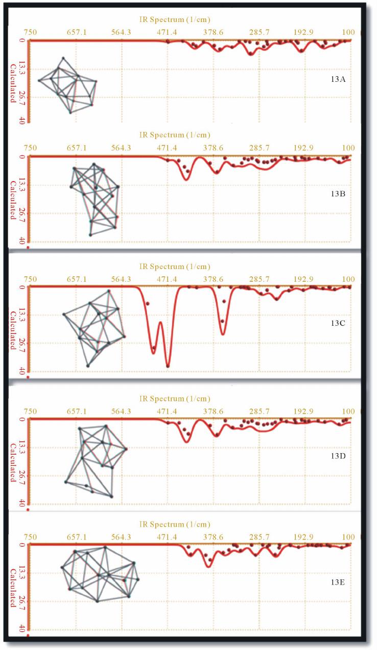 N. D. E. TORRES ET AL. 21 Figure 22. Structures and FTIR spectra calculated for isomers Si13 (13A to 13E). Open Access JMP  N. D. E. TORRES ET AL. Open Access JMP 22 Table 11. Optical and structural parameters calculated for isomers Si13. Isomer Energy [Hartree] Size [nm] rel. E (eV) BandGap [eV] Ovality PolarizabilityUV-Vis_ lambda max[nm] ZPVE [eV] Dipole [Debye] 13A −3763.34 0.7171138350.00 1.85408440 1.1686782665.9397550 1040.06464 0.552653862 1.75427983 13B −3763.33 0.7063466620.20 2.04189784 1.1929823966.3075238 831.133765 0.526377920 1.33654866 13D −3763.33 0.7062923530.20 2.04096395 1.1930290066.3048626 832.318003 0.526413642 1.34921474 13E −3763.32 0.7153297810.37 1.76424755 1.1774625366.3388454 676.653707 0.514426303 0.637141338 13C −3763.32 0.7116603330.39 2.23694992 1.1813224666.0842505 563.351931 0.545898936 1.78208642 dipole moment values (greater than 1.3 Debye). Average size of isomers Si13 is 0.71134 nm. Band gap average calculated over five isomers is 1.9876 eV. We can appre- ciate structural shapes in left inset 13A to 13E of Figure 22. Calculated luminescence for isomers Si13 is shown on Figure 23. For isomer 13A, the spectra calculated include two main peaks, one with emission in visible region (red) and another with the highest emission intensity in NIR (1040.064 cm−1). On both sides of the peaks there are shoulders with similar intensities, at 670.75nm and 1098.66nm, respec- tively. Isomers 13B and 13D are iso-energetic, and for this reason their UV-Vis spectra are quite similar. To appre- ciate numerical differences see Table 11. As we have said already, isomer 13C has the highest vibrations intensity and its luminescence spectra content two symmetric peaks. The highest local minimum corre- sponds to isomer 13C. Also, isomer 13C results with the highest band gap (2.237 eV) and dipole moment calcu- lated (1.782 Debye). Whereas that, the isomer 13E has the lowest band gap, ZPVE and dipole moment, and the emission in IR trends to disappear. 3.8. Structural and Optical Properties for Silicon Isomers Si14 For Si14 clusters, a number of low-lying isomers have been cited in the literature [16,17,37,39,47-50]. Isomer 14A (Cs) has two stacked rhombi with distortion and one five-fold ring capped with an atom. The vibrational frequency analysis done by Zhu et al. [15] indicates isomer 14A has one imaginary frequency. Ours results to not contain a transition state for this isomer. A structural perturbation followed by geometry relaxation gives isomer 14A bis (C1) which is very close in structure to 14A. 14A bis also ex- hibits a stacking sequence of two distorted rhombi, one five-fold ring, and an atom on top. General agreement is that the isomer 14A (Cs) found by Sieck et al. [39] is pos- sibly the global minimum. Ours calculus confirm isomer 14A as global minimum (see Table 12) sharing the pos- sibility to be global minimum with isomer 14A bis with an energy difference of only −0.00009 eV. Isomers 14B, 14C, and 14D all exhibit a stacking se- quence of three (distorted) rhombi with one atom at the top and another at the bottom. The vibrational frequency analysis indicates that isomer 14D has one imaginary frequency, it means that, this isomer is a transition state. Isomer 14E has a capped trigonal-prism unit and we ob- tain two imaginary frequencies for this isomer. Structures for isomers Si14 are included on insets Figures 24 and 25. Energy differences calculated for isomers 14A bis to 14E, respect to isomer 14A, are much higher than 0.4 eV. There are 36 freedom degrees for isomers Si14. Isomers with global minimum (14A and 14A bis) have the lowest vibration intensities, whereas isomer 14D which results to be a transition state, has the highest vibration intensity which corresponds to 393.601 cm−1. The highest emission expected for isomer 14A corre- sponds with green color (509.249 nm) and is quite similar to expected for isomer 14A bis (509.263 nm). Most of their properties are similar except may be the size. This pair of isomers will emit in a wide band from violet to green. Isomers 14B and 14C show a redshift and extend covering a great part of visible region, isomer 14D does not display detectable emission and isomer 14E will emit preferably in NIR. 4. Conclusions We have calculated low-energy nano-structures of Si7 - Si14 at the HF/6-31G(d) level of theory. The vibrational frequency analysis has been used to confirm the stability of the lowest-energy structures of Si7 - Si14 isomers. We employed FTIR calculated spectra in order to identify silicon agglomerates found in SRO film deposited by LPCVD. We evaluated different local energy isomers and we obtained the global isomers Si7 - Si14 (lowest-energy), and found energy differences less than 0.5 eV for most of isomers evaluated, except for Si14 in which the differences in energy are bigger. By plotting the binding energy per atom as a function of n−1/3 where n is the cluster size, for small agglomerates (Si7 - Si11), the binding energy per atom has an n−1/3 dependence, suggesting that small sili- con clusters trends spherical-like cluster growth. Haber- land proposed that the deviaon from the linear behavior ti 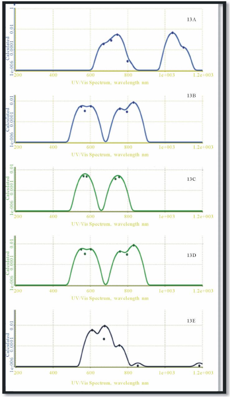 N. D. E. TORRES ET AL. 23 Figure 23. UV-Vis spectra calculated for isomers Si13 (13A to 13E). Open Access JMP 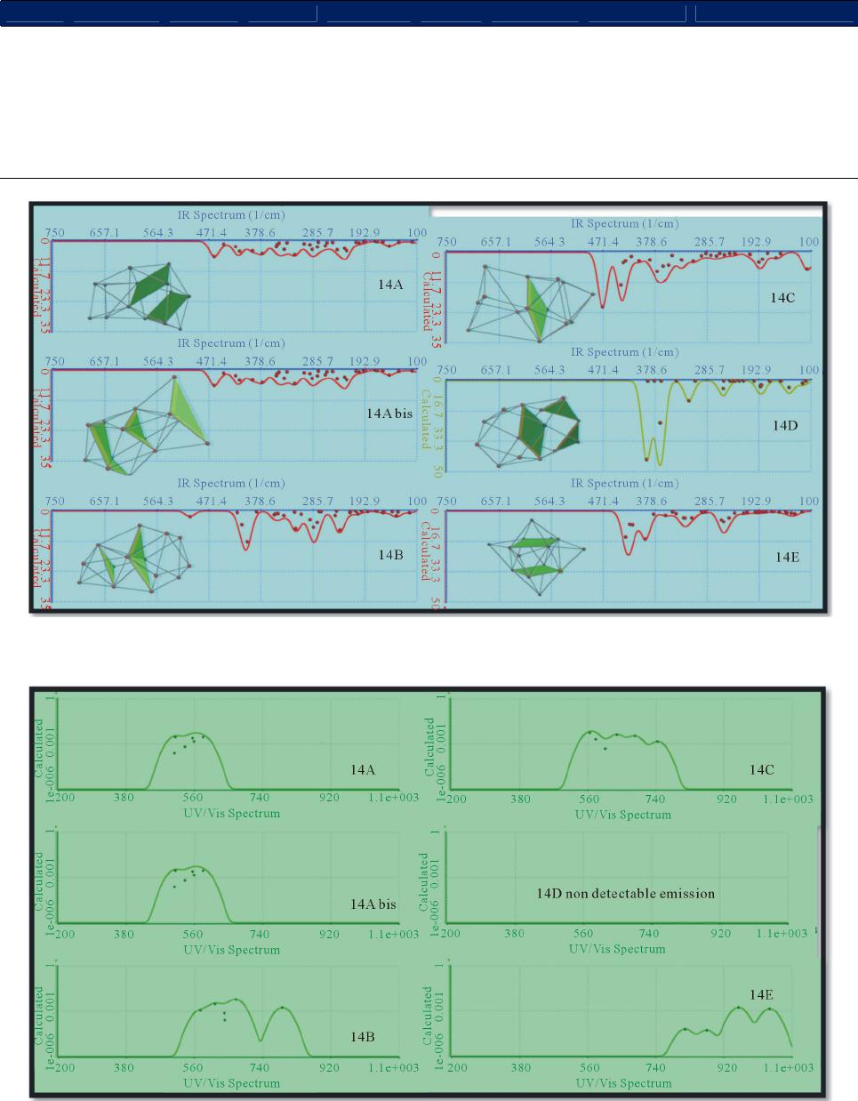 N. D. E. TORRES ET AL. 24 Table 12. Optical and structural parameters calculated for isomers Si14. Isomer E (au) rel. E (eV) Size[nm] BandGap eVOvality PolarizabilityDipole (debye) UVVIS_ LAMDAMAX 14A −4052.84522 0.00000 0.7266395 2.749521 1.18227167.65458 1.434 509.249 14A BIS −4052.84522 −0.00009 0.7184460 2.749496 1.18227167.65463 1.434 509.263 14B −4052.81350 0.86313 0.7223203 2.172161 1.18951767.80396 3.119 669.498 14C −4052.83006 0.41248 0.7125147 2.330958 1.21238468.20395 0.647 565.667 14D −4052.77424 1.93145 0.7382580 1.792246 1.16491967.96963 0.002 Non detectable emission 14E −4052.75299 2.50957 0.7145326 1.112898 1.20549568.25954 1.436 958.566 Figure 24. Structures and FTIR spectra calculated for isomers Si14. Isomer 14D with the highest frequency intensity, scale 0 - 50 (u.a.) for isomers 14D and 14E. Figure 25. UV-Vis spectra calculated for isomers Si14. Isomer 14D has not detectable emission. Open Access JMP  N. D. E. TORRES ET AL. Open Access JMP 25 for the binding energy versus n−1/3 curve suggests the growth pattern of the low-lying medium-sized (Si12 - Si14) clusters deviates from the spherical growth pattern [50]. This fact indicates that the low-lying Si7 - Si14 clusters follow a non-spherical growth pattern. Also, we note that the lowest-energy structures of Si12 - Si14 all contain the TTP Si9 unit. Although the TTP Si9 unit is not a stand- alone local minimum, it appears to be a favorable building block [38] for medium-sized clusters Si12 - Si14. We calculated UV-Vis spectra for isomers Si7 - Si14. We found that most of the silicon agglomerates with small and medium size (less than 1.0 nm) could emit in visible region and this is a transcendental fact; because up to now, it is not possible to detect experimentally nanoagglomer- ates with size less than 1.0 nm and could be an explantion for finding luminescence in SRO thin films with Ro = 30. 5. Acknowledgements This work has been partially supported by CONA- CyT-154725, PIFI-2013 and VIEP-BUAP-2013. N.D. Espinosa-Torres acknowledges the financial support of CONACYT by the scholarship given to carry out PhD studies, to VIEP and ICUAP-CIDS for support through PIFI 2012 projects and gives a special acknowledgment to the Academic Team: “Organic and Nano-structured Semi- conductors” for their invaluable support. REFERENCES [1] L. T. Canham, Applied Physics Letters, Vol. 57, 1990, p. 1046. http://dx.doi.org/10.1063/1.103561 [2] D. J. Lockwood, “Light Emission in Silicon,” In: D. J. Lockwood, Ed., Light Emission in Silicon from Physics to Devices. Semiconductors and Semimetales, Vol. 49, Aca- demic Press, San Diego, 1998. [3] Z. Z. Yuan, G. Pucker, A. Marconi, F. Sgrignuoli, A. Anopchenko, Y. Jestin, L. Ferrario, P. Bellutti and L. Pavesi, Solar Energy Materials and Solar Cells, Vol. 95, 2011, pp. 1224-1227. http://dx.doi.org/10.1016/j.solmat.2010.10.035 [4] N. D. Espinosa-Torres, J. F. J. Flores-Gracia, J. A. Luna- López, A. Morales-Sánchez, Ragnar Kiebach, J. C. Ramí- rez-García, D. Hernández de la Luz and E. Camacho- Espinosa. “In Silico Study of Electro-Luminescence in SRO thin Films due to [Sin-On],” Will be Published. [5] W. D. Knight, K. Clemenger, W. A. de Heer, W. A. Saunders, M. Y. Chou and M. L. Cohen, Physical Re- view Letters, Vol. 52, 1984, pp. 2141-2143. http://dx.doi.org/10.1103/PhysRevLett.52.2141 [6] K. Raghavachari and C. M. Rohlfing, The Journal of Chemical Physics, Vol. 89, 1988, p. 2219. http://dx.doi.org/10.1063/1.455065 [7] Y. H. Luo, J. J. Zhao and G. H. Wang, Physical Review B, Vol. 60, 1999, pp. 10703-10706. http://dx.doi.org/10.1103/PhysRevB.60.10703 [8] D. E. Bergeron and A. W. Castleman Jr., The Journal of Chemical Physics, Vol. 117, 2002, p. 3219. http://dx.doi.org/10.1063/1.1486439 [9] S. Yoo, X. C. Zeng, X. Zhu and J. Bai, Journal of Ameri- can Chemical Society, Vol. 125, 2003, pp. 13316-13317. http://dx.doi.org/10.1063/1.1690755 [10] M. V. Ramakrishna and A. Bahel, The Journal of Chemical Physics, Vol. 104, 1996, p. 9833. http://dx.doi.org/10.1063/1.471742 [11] A. Bahel and M. V. Ramakrishna, Physical Review B, Vol. 51, 1995, pp. 13849-13851. http://dx.doi.org/10.1103/PhysRevB.51.13849 [12] Rohlfing and K. Raghavachari, Chemical Physics Letters, Vol. 198, 1990, p. 521. [13] C. M. Rohlfing and K. Raghavachari, Chemical Physics Letters, Vol. 198, 1992, p. 521. [14] Z. Y. Lu, C. Z. Wang and K. M. Ho, Physical Review B, Vol. 61, 2000, pp. 2329-2334. http://dx.doi.org/10.1103/PhysRevB.61.2329 [15] X. Zhu and X. C. Zeng, The Journal of Chemical Physics, Vol. 118, 2003, p. 3558. http://dx.doi.org/10.1063/1.1535906 [16] K.-M. Ho, A. A. Shvartsburg, B. Pan, Z.-Y. Lu, C.-Z. Wang, J. G. Wacker, J. L. Fye and M. F. Jarrold, Nature, Vol. 392, 1998, pp. 582-585; http://dx.doi.org/10.1038/33369 [17] B. Liu, Z.-Y. Lu, B. Pan, C.-Z. Wang, K.-M. Ho, A. A. Shvartsburg and M. F. Jarrold, The Journal of Chemical Physics, Vol. 109, 1998, p. 9401. http://dx.doi.org/10.1063/1.477601 [18] I. Rata, A. A. Shvartsburg, M. Horoi, T. Frauenheim, K. W. M. Siu and K. A. Jackson, Physical Review Letters, Vol. 85, 2000, pp. 546-549. http://dx.doi.org/10.1103/PhysRevLett.85.546 [19] B.-X. Li, P.-L. Cao and S.-C. Zhan, Physics Letters A, Vol. 316, 2003, pp. 252-260. http://dx.doi.org/10.1016/S0375-9601(03)01173-3 [20] O. Guillois, N. Herlin-Boime, C. Reynaud, G. Ledoux, F. Huisken, Journal of Applied Physics, Vol. 95, 2004, p. 3677. http://dx.doi.org/10.1063/1.1652245 [21] M. Aceves-Mijares, A. A. González-Fernández, R. López- Estopier, A. Luna-López, D. Berman-Mendoza, A. Morales, C. Falcony, C. Domínguez and R. Murphy-Arteaga, Journal of Nanomaterials, Vol. 2012, 2012, Article ID: 890701. http://dx.doi.org/10.1155/2012/890701 [22] Al. L. Efros and A. L. Efros, Soviet Physics: Semicon- ductors, Vol. 16, 1982, p 1209. [23] S. V. Gaponenko, “Optical Properties of Semiconductor Nanocrystals,” Cambridge University Press, Cambridge, 1998. [24] L. E. Brus, The Journal of Chemical Physics, Vol. 80, 1984, p. 4403. http://dx.doi.org/10.1063/1.447218 [25] Y. Kayanuma, Physical Review B, Vol. 38, 1988, pp. 9797-9805. http://dx.doi.org/10.1103/PhysRevB.38.9797 [26] L. Dal Negro, M. Cazzanelli, L. Pavesi, S. Ossicini, D. Pacifici, G. Franzò, F. Priolo and F. Iacona, Applied  N. D. E. TORRES ET AL. 26 Physics Letters, Vol. 82, 2003, pp. 4636-4638. http://dx.doi.org/10.1063/1.1586779 [27] A. Meldrum, R. F. Haglund Jr., L. A. Boatner and C. W. White, Advanced Materials, Vol. 13, 2001, pp. 1431-1444. http://dx.doi.org/10.1002/1521-4095(200110)13:19<1431 ::AID-ADMA1431>3.0.CO;2-Z [28] M. H. Nayfeh, S. Rao, N. Barry, J. Therrien, G. Belomoin, A. Smith and S. Chaieb, Applied Physics Letters, Vol. 80, 2002, pp. 121-123. http://dx.doi.org/10.1063/1.1428622 [29] M. Zacharias, J. Heitmann, R. Scholz, U. Kahler, M. Schmidt and J. Bläsing, Applied Physics Letters, Vol. 80, 2002, pp. 661-663. http://dx.doi.org/10.1063/1.1433906 [30] J. Wang, X. F. Wang, Q. Li, A. Hryciw and A. Meldrum, Philosophical Magazine, Vol. 87, 2007, pp. 11-27. http://dx.doi.org/10.1080/14786430600863047 [31] C. Delerue, G. Allan and M. Lannoo, Journal of Lumi- nescence, Vol. 80, 1998, pp. 65-73. http://dx.doi.org/10.1016/S0022-2313(98)00071-4 [32] V. A. Belyakov, V. A. Burdov, R. Lockwood and A. Meldrum, Advances in Optical Technologies, Vol. 2008, 2008, Article ID: 279502. http://dx.doi.org/10.1155/2008/279502 [33] J. A. Luna-López, G. García-Salgado, T. Díaz-Becerril, J. Carrillo López, D. E. Vázquez-Valerdi, H. Juárez-Santies- teban, E. Rosendo-Andrés and A. Coyopol, Materials Science and Engineering B, Vol. 174, 2010, pp. 88-92. http://dx.doi.org/10.1016/j.mseb.2010.05.005 [34] E. C. Honea, A. Ogura, C. A. Murray, K. Raghavachari, W. O. Sprenger, M. F. Jarrold and W. L. Brown, Nature, Vol. 366, 1993, pp. 42-44. http://dx.doi.org/10.1038/366042a0 [35] X. L. Zhu, X. C. Zeng, Y. A. Lei, and B. Pan, The Jour- nal of Chemical Physics, Vol. 120, 2004, p. 8985. http://dx.doi.org/10.1063/1.1690755 [36] X. L. Zhu and X. C. Zeng, The Journal of Chemical Physics, Vol. 118, 2003, p. 3558. http://dx.doi.org/10.1063/1.1535906 [37] I. H. Lee, K. J. Chang and Y. H. Lee, Journal of Physics: Condensed Matter, Vol. 6, 1994, p. 741. http://dx.doi.org/10.1088/0953-8984/6/3/014 [38] K. M. Ho, A. A. Shvartsburg, B. Pan, Z. Y. Lu, C. Z. Wang, J. G. Wacker, J. L. Fye and M. F. Jarrold, Nature, Vol. 392, 1998, p. 582. http://dx.doi.org/10.1038/33369 [39] A. Sieck, D. Porezag, Th. Frauenheim, M. R. Pederson and K. Jackson, Physical Review A, Vol. 56, 1997, pp. 4890-4898. http://dx.doi.org/10.1103/PhysRevA.56.4890 [40] I. Vasiliev, S. Ogut and J. R. Chelikowsky, Physical Re- view Letters, Vol. 78, 1997, pp. 4805-4808. http://dx.doi.org/10.1103/PhysRevLett.78.4805 [41] D. J. Wales, Physical Review A, Vol. 49, 1994, pp. 2195- 2198. http://dx.doi.org/10.1103/PhysRevA.49.2195 [42] C. M. Rohlfing and K. Raghavachari, Chemical Physics Letters, Vol. 167, 1990, p. 559. http://dx.doi.org/10.1016/0009-2614(90)85469-S [43] C. M. Rohlfing and K. Raghavachari, The Journal of Chemical Physics, Vol. 96, 1992, p. 2114. http://dx.doi.org/10.1063/1.462062 [44] H. Jahn and E. Teller, Proceedings of the Royal Society of London Series A, Mathematical and Physical Sciences (1934-1990) , Vol. 161, 1937, pp. 220-235. http://dx.doi.org/10.1098/rspa.1937.0142 [45] B.-L. Gu, Z.-Q. Li and J.-L. Zhu, Journal of Physics: Condensed Matter, Vol. 5, 1993, p. 5255. http://dx.doi.org/10.1088/0953-8984/5/30/005 [46] J. C. Grossman and L. Mitas, Physical Review Letters, Vol. 74, 1995, pp. 1323-1326. http://dx.doi.org/10.1103/PhysRevLett.74.1323 [47] B. X. Li, P. L. Cao and M. Jiang, Physica Status Solidi B, Vol. 218, 2000, pp. 399-400. http://dx.doi.org/10.1002/1521-3951(200004)218:2<399:: AID-PSSB399>3.0.CO;2-R [48] B. X. Li and P. L. Cao, Physical Review A, Vol. 62, 2000, Article ID: 023201. http://dx.doi.org/10.1103/PhysRevA.62.023201 [49] B. X. Li and P. L. Cao, Journal of Physics: Condensed Matter, Vol. 13, 2001, p. 1. http://dx.doi.org/10.1088/0953-8984/13/1/301 [50] H. Haberland, “Clusters of Atoms and Molecules: Theory, Experiment, and Clusters of Atoms,” Springer, New York, 1994. Open Access JMP
|