Journal of Computer and Communications, 2013, 1, 23-26
Published Online December 2013 (http://www.scirp.org/journal/jcc)
http://dx.doi.org/10.4236/jcc.2013.17006
Open Access JCC
23
Simulation and Design of a Submicron Ultrafast Plasmonic
Switch Based on Nonlinear Doped Silicon MIM Waveguide
Ahmad Naseri Ta heri, Hassan Kaatuzian
Photonics Research Laboratory (PRL), Electrical Eng. Dept, Amirkabir University of Technology, Tehran, Iran.
Email: ahmadnaseri@aut.ac.ir, hsnkato@aut.ac.ir
Received September 2013
ABSTRACT
We propose and analyze a submicron stub-assisted ultrafast all-optical plasmonic switch based on nonlinear MIM wa-
veguide. It is constructed by two silicon stub filters sandwiched by silver cladding. The signal wavelength is assumed to
be 1550 nm. The simulation results show a 14.66 dB extinction ratio. Downscaling the silicon waveguide in MIM
structure leads to enhancement of the effective Kerr nonlinearity due to tight mode confinement. Also, using O+ ions
implanted into silicon, the switching time less than 10 ps and a delay time less than 8 fs are achieved. The overall length
of the switch is 550 nm.
Keywords: Plasmonics; Silicon Based All-Op tical Switch; S tub Filter; Metal-Insulator-Metal Waveguide; Nonlinear
Kerr Effect
1. Introduction
Plasmonics promises the speed of light in nano-scale inte-
gration to the future of data processing and communica-
tions [1,2]. The combined advantages of ultrafast optical
signal processing capabilities of photonics and the feasi-
bility of nano-scale fabrication motivate researchers to
work on Plasmonics [3-5]. In the past years, many tech-
niques and devices in the field of Plasmonics are devel-
oped. Among those, Metal-Insulator-Metal (MIM) plas-
monic waveguides provided many applications, because
their mode confinement in deep subwavelength scale and
high group velocity extended over wide range of frequen-
cies, from DC to visible. Several applications of MIM
plasmonic waveguides such as filters, Bragg Reflectors,
modulators, and switches are reported [6-9]. In some of
reports, remarkable properties of nonlinear Surface Plas-
mon Polariton: (SPP)-based structures are utilized to pro-
pose nanophotonic devices [8,10]. In order to eliminate
the limit in switching speed due to electronics, all-optical
methods are developed [11,12]. In most of the all-optical
switching methods, a pump signal alters the refractive
index of the path of another signal and changes its phase
or intensity [12]. However, because of weak nonlinear
properties of medium, they need more powerful pump
and/or longer nonlinear waveguide for more effective
interaction. In addition, the separation of data signal fro m
pump signal requires an external filter in which increases
the overall length of the switch. Stub structures have been
used as wavelength selective filter in plasmonic wave-
guides [13,14]. A stub has good filtering effect for dis-
crete wavelengths.
In this paper, we propose an all-optical switch based
on Metal-Insulator-Metal plasmonic structure and uti-
lized two stub filters, one as active mediu m and the other
as output filter. Silver-doped silicon is used as active
material, in which reported to have giant Kerr nonlinear-
ity n2 = 1.47 × 10⁹ m2/W [15]. We have used a periodic
stub as Bragg reflector in order to filter control signal
from data signal. Also, we have employed another peri-
odic stub filter as an active region of our switch. Chang-
ing the refractive index of this periodic stub converts it
into 1550 nm filter. The overall length of our switch is
550 nm. Our design has numerically investigated based
upon 2-D Finite Element Method simulations using
COMSOL Multiphysics. In Section 2, we’ll describe in
brief, how a MIM plasmonic waveguide works. In Sec-
tion 3, nonlinear Kerr effect in our proposed stub struc-
ture and its switching applications will be explained. In
Section 4, we’ll present the simulation results obtained in
our plasmonic switch design. We’ll also have a conclu-
sion section.
2. MIM Plasmonic Waveguide
In spite of the severe loss, among the other schemes of
Simulation and Design of a Submicron Ultrafast Plasmonic Switch Based on Nonlinear Doped Silicon MIM Waveguide
Open Access JCC
24
plasmonic waveguides, MIM has the advantage of strong
modal confinement in its subwavelength size. In this struc-
ture, two SPP’s couple into the centr al dielectric slot and
thus give s rise to a huge field concentrati on.
Figure 1 shows a schematic diagram of a Metal-Insu-
lator-Metal waveguide. In this type of plasmonic wave-
guide a dielectric core is surrounded by two metal clad-
dings. The dispersion relation of this waveguide described
by [6]:
tanh 2
md d
mm
kk tk
εε

= −

(1)
Where
d
ε
dielectric constant of dielectric core,
m
ε
the dielectric function of metal cladding, and
d
k
and
m
k
are the transverse wave number in the core and the
cladding, respectively. We use a seven-pole Drude-Lo-
rentz model, in which is defined in the wavelength range
from 0.2 to 2 μm [16]:
( )( )
22
5
222
1
1
pnn
nn
f
iin
ωω
εω ωω γω ωωγ
=
=−+
+−−
(2)
Where, ωp = 2002.6 TH z is the bulk plasma frequency
of silver a nd γ = 11.61 THz is a damping constant. Other
parameters are listed in the Table 1. In all our simula-
tions we applied the above model to create more accurate
results.
3. Kerr Effect in Stub Structure
One of the common elements between microwave engi-
neering and photonics is the stub structure which is uti-
lized as wavelength selective filter. Many reports numer-
ically demonstrate stub structures as compact size and
simple filter [14]. A stub filter consists of one or more
finite length waveguide(s) perpendicular to the main wa-
veguide.
Figure 1. Schematic diagram of a metal-insulator-metal
waveguide.
In our switch, we have employed two different stub
filters, at input and output. Both of them have been sepa-
rately simulated to obtain their transmission spectrum.
Changing three parameters (mentioned in Table 1), could
change the spectrum of the filter, the length of stub(s),
the width of stub(s) and/or the refractive index of the
core. For changing the transmission characteristics of this
Silicon based plasmonic switch in “ON” and “OFF” states,
we propose to use Silver-doped Silicon. So that nonlinear
optical Kerr effect may be observed during 1550 nm sig-
nal switching using 1000 nm pump. Kerr occurs, when
the Si waveguide is subjected to a strong pump field (E).
It becomes doubly refracting. So the refractive index will
be changed as follows [17,18]:
(3)
Utilizing nonlinear optical Kerr effect in silicon (the
core of MIM waveguide and stub(s)), and based on fem-
tosecond optical perturbation, we can change the refrac-
tive index of the MIM waveguide and therefore by shift-
ing the transmission spectrum of the stub at 1550 nm, the
switchi n g process would be achi e ved.
Figures 2(a) and ( b) show the transmission of two fil-
ters vs. wavelength. The input stub filter should pass
1550 nm signal and 1000 nm pump. Also, by reasonable
small changing the refractive index, this filter attenuates
1550 nm signal. Therefore, the length of stubs of this
filter is selected Ls1 = 450 nm.
The second stub, as shown in Figure 2(b), acts stati-
cally and only filters the 1000 nm pump signal. The
length of its stubs is chosen so that it passes the 1550 nm
signal and reflects the 1000 nm pump. Therefore, based
on simulations we have chosen the length of this stub
filter Ls2 = 200 nm.
Table 1. Parameters Of The Drude-Lorentz Model For Sil-
ver [16].
n ωn(THz) γn(THz) fn
1 197.3 939.62 7.9247
2 1083.5 109.29 0.5013
3 1979.1 15.71 0.0133
4 4392.5 221.49 0.8266
5 9812.1 584.91 1.1133
Figure 2. Transmission spectrum of (a) input filter with 400 n, stub Length and (b) output filter with 2000 nm stub length.
Simulation and Design of a Submicron Ultrafast Plasmonic Switch Based on Nonlinear Doped Silicon MIM Waveguide
Open Access JCC
25
The number of stubs in each filter depends on their
functionality. In the first filter, we need to increase the
effective length of the nonlinear region. So, three stubs
design is proposed. But in second filter, two stubs are
enough to reject the control beam from output.
4. Plasmonic Switch Simulation Results
Figure 3 depicts the proposed MIM plasmonic all-optical
switch. It consists of a silicon waveguide sandwiched by
silver.
The width of main waveguide and stubs of two filters
is selected W = 50 nm and the length of stubs of the input
filter is Ls1 = 450 nm and the output filter Ls2 = 200 nm
and the distance of them is d = 100 nm. The overall length
of the switch is L = 550 nm. That means, our switch has
subwavelength dimension. Figures 4(a)-(c) demonstrate
the field distribution in the switch. As seen in Figures
4(a) and (c), in on-state the 1550 nm signal passes both
filters and 1000 nm pump passes the input filter and
changes its refractive index and reflected by second one.
In off-state, after modifying refractive index of first filter,
the 1550 nm signal is filtered and reflected to the input
(Figure 4(b)). The overall transmission of the switch in
ON and OFF state is shown in Figure 5. Imposing the
control signal, the stop band of the control pulse (1000
nm) is almost remained unchanged; however, the trans-
mission of the switch falls at 1550 nm.
Ion-Implanted Silicon (II-Si) helps the switching process
in ultrafast sweeping the excited free-carriers in less than
10 fs [11,12]. Simulations show an 8 fs delay time for the
Figure 3. The proposed structure utilizing two stub filters
based on MIM plasmonic waveguide.
Figure 4. Intensity distribution of (a) 1550 nm at “on” state
(b) 1550 nm at “off” state (c) 1000 nm as pump signal.
optical pulse to pass the switch (Figure 6). Figure 7 de-
picts the ou tput power of 1550 nm signal respect to pow-
er of 1000 nm pump power. The extinction ratio is cal-
culated 14.66 dB.
5. Conclusion
In this paper, the all-optical plasmonic switch based on
metal-insulator-metal structure is des igned and simulated.
In the structure of the switch, two stub filters are embed-
ded. These filters are designed and analyzed to perform
with the communication wavelength 1550 nm. Th e sma ll
Figure 5. The overall transmission of the switch in OFF
(dashed) and ON (solid) state.
Figure 6. The temporal simulation of the switch shows a 8 fs
delay in response.
Figure 7. Dependence of Output power of the 1550 nm sig-
nal to power of the 1000 nm pump.
d
L
W
L
s1
W
L
s2
(a) (b)(c)
Simulation and Design of a Submicron Ultrafast Plasmonic Switch Based on Nonlinear Doped Silicon MIM Waveguide
Open Access JCC
26
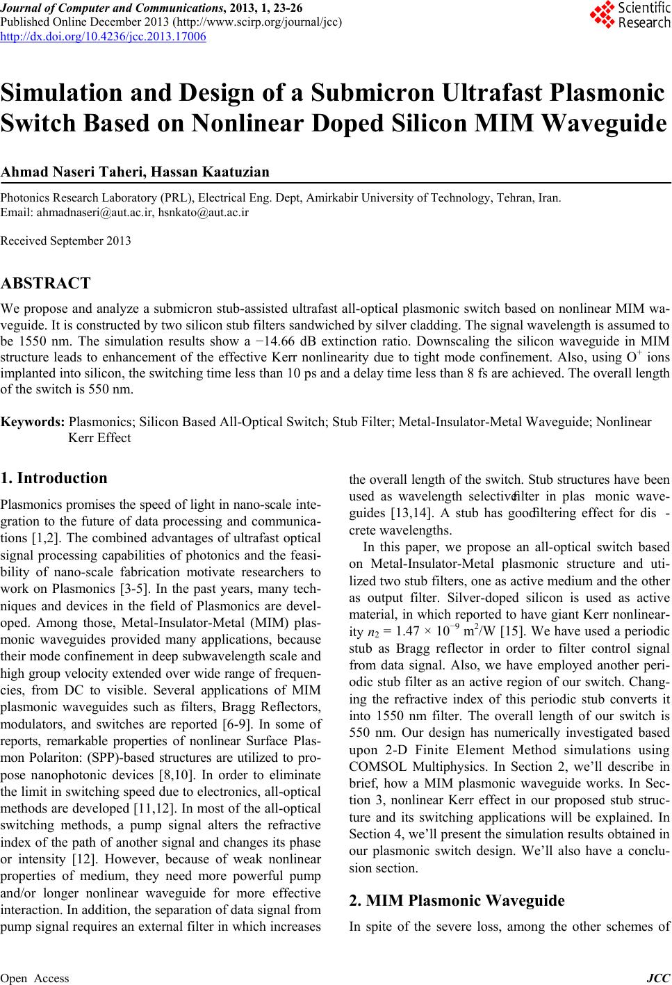
dimension of the switch (550 nm) is the main interest in
reduction of the loss. It means that this plasmonic device
will be more suitable for designing high dense integrated
optical devices. Using F inite Element Method (FEM) the
operation of the switch is investigated. The overall length
of the switch is 550 nm and extinction ratio is 14.66 dB.
REFERENCES
[1] R. Zia, J. A. Schuller, A. Chandran and M. L. Brongers-
ma, “Plasmonics: The Next Chip-Scale Technology,
Materials Today, Vol. 9, 2006, p. 20.
http://dx.doi.org/10.1016/S1369-7021(06)71572-3
[2] D. K. Gramotnev and S. I. Bozhevolnyi, “Plasmonics be-
yond the Diffraction Limit,Nature Photonics, Vol. 4,
2010, pp. 83-91.
http://dx.doi.org/10.1038/nphoton.2009.282
[3] W. L. Barnes, A. Dereux and T. W. Ebbesen, “Surface
Plasmon Subwavelength Optics,” Nature, Vol. 424, 2003,
pp. 824-830. http://dx.doi.org/10.1038/nature01937
[4] T. W. Ebbesen, C. Genet and S. I. Bozhevolnyi, “Surface-
Plasmon Circuitry,Physics Today, Vol. 61, 2008, pp.
44-50. http://dx.doi.org/10.1063/1.2930735
[5] S. A. Maier, Plasmonics: The Promise of Highly Inte-
grated Optical Devices,IEEE Journal of Selec ted Topics
in Quantum Electronics, Vol. 12, 2006, p. 1671.
http://dx.doi.org/10.1109/JSTQE.2006.884086
[6] J. Park, H. Kim and B. Lee, High Order Plasmonic
Bragg Reflection in the Metal-Insulator-Metal Waveguide
Bragg Grating,” Optics Express, Vol. 16, No. 1, 2008.
http://dx.doi.org/10.1364/OE.16.000413
[7] Y. Chang, Design and Analysis of Metal/Multi-Insulator/
Metal Waveguide Plasmonic Bragg grating,Optics Ex-
press, Vol. 18, No. 12, 2010.
http://dx.doi.org/10.1364/OE.18.013258
[8] N. Nozhat and N. Granpayeh, “Switching Power Reduc-
tion in the Ultra-Compact Kerr Nonlinear Plasmonic Di-
rectional Coupler,” Optics Communications, Vol. 285,
2012, pp. 1555-1559.
http://dx.doi.org/10.1016/j.optcom.2011.11.110
[9] L. Sweatlock and K. Diest, “Vanadium Dioxide Based
Plasmonic Modulators,” Optics Express, Vol. 20, No. 18,
2012.
[10] M. Pu, N. Yao, C. Hu, X. Xin, Z. Zhao, C. Wang and X.
Luo, “Directional Coupler and Nonlinear Mach-Zehnder
Interferometer Based on Metal-Insulator-Metal Plasmonic
Waveguide,” Optics Express, Vol. 18, No. 20, 2010, p.
21030. http://dx.doi.org/10.1364/OE.18.021030
[11] A. Y. Elezzabi, Z. Han, S. Sederberg and V. Van, “Ultra-
fast All-Optical Modulation in Silicon-Based Nanoplas-
monic Devices,” Optics Ex press, Vol. 17, No. 13, 2009, p.
11045,. http://dx.doi.org/10.1364/OE.17.011045
[12] S. Sederberg, D. Driedger, M. Nielsen and A. Y. Elezzabi,
Ultrafast All-Optical Switching in a Silicon-Based Plas-
monic Nanoring Resonator,” Optics Express, Vol. 19, No.
2, 2011.
[13] J. Liu, G. Fang, H. Zhao, Y. Zhang and S. Liu, “Surface
Plasmon Reflector Based on Serial Stub Structure,” Op-
tics Express , Vol. 17, No. 22, 2009.
http://dx.doi.org/10.1364/OE.17.020134
[14] N. Zhu, T. Mei, Analysis of an Ultra-Compact Wave-
length Filter Based on Hybrid Plasmonic Waveguide
Structure,” Optics Letters, Vol. 37, No. 10, 2012.
http://dx.doi.org/10.1364/OL.37.001751
[15] J. Wei, J. Liu and M. Xiao, Giant Optical Nonlinearity
of Silver-Doped Silicon Thin Film at Low Power Input:
Laser-Triggered Cluster Resonance,” Applied Physics A,
2011, pp. 1031-1037.
http://dx.doi.org/10.1007/s00339-011-6464-3
[16] A. Pannipitiya, I. D. Rukhlenko, M. Premaratne, H. T.
Hattori and G. P. Agrawal, “Improved Transmission Mo-
del for Metal-Dielectric-Metal Plasmonic Waveguides
with Stub Structure, Optics Express, Vol. 18, No. 6, 2010.
http://dx.doi.org/10.1364/OE.18.006191
[17] F. A. Jenkins and H. E. Whit e, Fundamentals of Optics,
4th Edition, McGraw-Hill, 1981.
[18] H. Kaat uzian, “Photonics,” Vol. 1, 2nd Edition, AUT Press,
in Persian, 2008.