 Advances in Materials Physics and Chemistry, 2013, 3, 299-306 Published Online November 2013 (http://www.scirp.org/journal/ampc) http://dx.doi.org/10.4236/ampc.2013.37041 Open Access AMPC Effect of Switching on Metal-Organic Interface Adhesion Relevant to Organic Electronic Devices Babaniyi Babatope1*, Akogwu Onobu2, Olusegun O. Adewoye3, Winston O. Soboyejo2,3 1Department of Physics, Obafemi Awolowo University, Ile-Ife, Nigeria 2Department of Mechanical and Aerospace Engineering, Princeton University, Princeton, USA 3Materials Science and Engineering Department, African University of Science and Technology, Abuja, Nigeria Email: *niyibabatope@gmail.com Received September 4, 2013; revised October 8, 2013; accepted October 16, 2013 Copyright © 2013 Babaniyi Babatope et al. This is an open access article distributed under the Creative Commons Attribution Li- cense, which permits unrestricted use, distribution, and reproduction in any medium, provided the original work is properly cited. ABSTRACT Considerable efforts are currently being devoted to investigation of metal-organic, organic-organic and organic-inor- ganic interfaces relevant to organic electronic devices such as organic light emitting diode (OLEDs), organic photo- voltaic solar cells, organic field effect transistors (OFETs), organic spintronic devices and organic-based Write Once Read Many times (WORM) memory devices on both rigid and flexible substrates in laboratories around the world. The multilayer structure of these devices makes interfaces between dissimilar materials in contact and plays a prominent role in charge transport and injection efficiency which inevitably affect device performance. This paper presents results of an initial study on how switching between voltage thresholds and chemical surface treatment affects adhesion prop- erties of a metal-organic (Au-PEDOT:PSS) contact interface in a WORM device. Contact and Tapping-mode Atomic Force Microscopy (AFM) gave surface topography, phase imaging and interface adhesion properties in addition to SEM/EDX imaging which showed that surface treatment, switching and surface roughness all appeared to be key fac- tors in increasing interface adhesion with implications for increased device performance. Keywords: AFM; Interface; Adhesion Force; Organic Electronics; Voltage Switching; Organic Memory Devices; Surface Treatment 1. Introduction The investigation of interfaces between dissimilar or- ganic-metal, organic-organic and organic-inorganic ma- terials which are inherent in the devices made from them has been intensified in recent times. The interface phe- nomena are thus crucial towards the development, under- standing and improvement of organic-based semicon- ductor electronic device [1-14] applications such as or- ganic light emitting devices (OLEDs) [15-18], organic photovoltaic devices [19-21], organic thin film transistor devices [22-27] and organic spin electronic devices in which the transport and control of spin polarized infor- mation are represented [28-30]. The interface between the different materials that make them up determines the charge transport and charge injection efficiency, with implications for the performance of the devices. Interfacial phenomena are particularly crucial towards the development and improvement of applications of these devices and in order to effectively investigate mul- tilayer structured devices, the overall flexibility becomes very critical. This, in addition to their molecular nature, makes the study of organic thin films interfaces to be more intensified compared to inorganic semiconductors. The type of interaction at the interface is either physi- cal or chemical and progress in organic electronics re- quires their detail understanding [31]. Investigations of the chemical nature of interfaces are common in thin film characterization, but not much attention has been directed at measuring physical interaction until recently when advanced characterization tools are becoming more widely available. However, in a work reported on the nanoscale adhesion between organic-organic, organic-inorganic, and inorganic-inorganic thin film interfaces [32], the AFM technique was used in quantifying the interfaces, though with some limitations. The pull-off forces and surface parameters were measured and incorporated into theo- *Corresponding author. 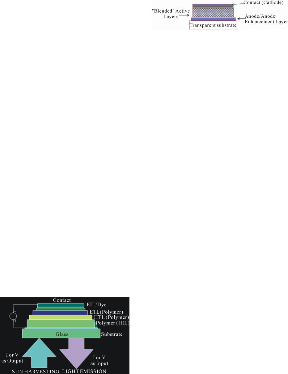 B. BABATOPE ET AL. 300 retical models for the estimation of surface energies. Ob- viously, therefore, the improvement of performance of organic electronic devices depends on a clear under- standing of the principles underlying organic-film/metal- electrode interfaces. Data-storage and switching applications of conjugated polymer-based devices in which, depending on the volt- age-sweep direction, two different current-voltage (I-V) characteristics, and hence low and high conducting states are used, have been observed and reported (e.g. [33-39]). These devices have an associated memory effect for data-storage applications especially the bistable archi- tectures (e.g. [21,26,38,40-47]). The bistable and multi- ple-layer stacking structures have therefore emerged as a viable technology for flexible, ultrafast, and ultrahigh- density memory devices in the field of organic electron- ics [48]. In a multilayer organic electronic device structure (Figure 1), charges often move from one layer to another by either injecting holes and/or electrons or transporting the same in one direction or the other. In the emissive layers, injected charges produce localized charge carry- ing species which move through the device under the influence of external field (bias) across the interface [49]. Charge injection transport efficiency through the inter- faces is thus critical to device performance. However, there are problems of adhesion, morphological inho- mogeneities and conductivity anisotropy at these inter- faces which are not yet properly understood [50]. Charge transport efficiency could be enhanced by re- ducing the number of interfaces in organic devices. This is often done using the standard polymer processing method of blending in which organic materials, forming individual layers, are innovatively blended, thereby re- ducing the number of layers. This has been recognized as one of the possible ways forwarded for improved charge transport efficiency [51], as illustrated in Figure 2. This investigation was therefore motivated by the need to explore additional interface reengineering techniques Figure 1. Typical device structure for sun harvesting (Poly- mer Solar Cells) and light emission (OLEDs). The figure shows the contacts and the emissive layers made up of dif- ferent carefully selected conducting (conjugated) polymers. Figure 2. Device structure that reduced the number of in- terfaces using conventional polymer blending technique in which each phase would be expecte d to independently their different roles of charge transportation and injection. using a combination of memory switching, adhesion and surface treatment. Also, this type of study could be in- corporated into device performance improvement studies in view of recent reported improving power conversion efficiency of conjugated polymer-based solar cells [52], which remains largely unsatisfactory for large-scale commercial production in competition with its amor- phous silicon-based devices. There are indications that charge transportation at the interface could be improved by a better understanding of the physical phenomena at the interface [32]. This has brought into the fore, an in- tensified investigation of the physical interaction be- tween the dissimilar materials in direct contact, which is vital to sustainable device performance. 2. Experimental Details 2.1. Materials and Equipment The materials used in this investigation include AL 4083 PEDOT:PSS suitable for OLED fabrication (H. C. Starck, MA, Newton, USA) as the organic layer, n-doped silicon wafer (Eagle-Picher, Miami, OK, USA) as the substrate, gold (Au) as the metal contact layer (Alfa Aesar, USA), hydrochloric acid (Aldrich, USA) for the surface treat- ment of the organic layer, Hydrofluoric acid (Aldrich, USA) and standard assorted reagents for substrate clean- ing. The thermal deposition of the gold contact on the organic layer was carried out using an Edwards E306A deposition system (Edwards, Sussex, UK), the switching was done with an HP semiconductor parameter analyzer (HP 4145B) for the current-voltage measurement, etched silicon contact AFM tips were purchased from Veeco Instruments (Woodbury, NY, USA), Digital Instruments Dimension 3000 Atomic Force Microscope (AFM) (Digital Instruments, Plainview, NY), Scanning Electron Microscope (SEM-EDX) (Philips FEI XL30 FEG-SEM, Hillsboro, USA), a standard Fishers ultrasonic bath, an ultra violet ozone cleaning system and a drying chamber were all used in the course of this study. 2.2. Experimental Procedure A Write Once Read Many times (WORM) device was fabricated by direct spin-casting of PEDOT:PSS on a suitably cleaned n-Si substrate followed by vacuum deposition of Au Contact. The cleaning procedure for the Open Access AMPC B. BABATOPE ET AL. 301 substrate includes the use of a combination of different solvents including acetone, trichloroethylene (TCE), iso- propanol, hydrofluoric acid (HF), a detergent and deion- ized water under different temperature conditions in an ultrasonic bath. The substrate was then transferred to an ultra violet ozone cleaning system for 5 min for further cleaning after which it was transferred to a glove box for safe keeping, ready for spin coating of the organic layer. A thin layer of PEDOT:PSS (about 500 nm) deter- mined based on standard calibration curves obtained by plotting series of spinning speeds, accelerations and thicknesses and after drying (H. C. Starck, Newton, MA USA suppliers of PEDOT:PSS) was then deposited on the substrate by spin coating in ambient air condition followed by baking in an oven at 200˚C for about 60 min. The sample was again transferred to a glove box ready for the Au deposition. Some of the spin-coated samples were chemically treated with dilute HCl (0.1 N) prior to deposition of the Au contact (approximately 100 nm, preceded by a thin layer, about 5 nm, of Cr) which was carried out by thermal evaporation under a vacuum of 1 × 10⁻⁶ Torr (1 Torr = 133.32 Pa). A selection of the Au/PEDOT:PSS/Si device was qua- sistatically switched or “blown” using a pulsed voltage ramp with 10 ms long 100 mV steps and applied for 0.5 - 4 ms as necessary The switching was carried out by use of current transients to change the polymer fuse (PE- DOT:PSS) from a conducting (“1” or “ON”) to a non- conducting (“0” or “OFF”) state. Quasistatic (continuous) condition (J~10 A/cm2): 0 V - 10 V - 0 V and rapid volt- age pulsed transient condition (J~1 kA/cm2): 10 V, 2 μs were used for this purpose [53,54]. The Au contact was deposited either before or after the polymer surface treatment and was carefully removed by a peeling process before and after switching. The same was done before and after polymer surface treatment. Phase imaging, surface topography and force calibration curves were obtained for the different surfaces by AFM in contact and tapping modes to quantify the physical interaction at the polymer interface using Au-coated can- tilever tips. Interaction force response between the sam- ple and cantilever tip [32,55] was measured for each sample. The surface roughness for each surface was re- corded and related to adhesion data as measured by the deflection as recorded from the interaction between Au-coated cantilever tip and the polymer surface. The differently deposited, treated or untreated, switched or unswitched surfaces before or after peeling the Au- contact, were separately investigated by SEM/EDX to qualitatively correlate the effectiveness of the peeling process, and the relative degree of polymer-metal inter- face adhesion. These tips were coated with Au the com- plementary materials that make direct contact with the surfaces. The purpose is also to investigate whether part of the polymer peeled with the gold contact. 3. Result and Discussion Figures 3 and 4 show the surface topography (Figures 3(a)-(d)) as determined by the degree of roughness ob- tained in the tapping mode; and the force calibration plots (Figures 3(a)-(d)) obtained in contact mode for the unswitched (Figures 4(a) and (c)) and switched (Figures 3(b) and (d)) devices when untreated (Figure 3) and treated (Figure 4). The values for the respective rough- ness are as shown in Table 1. Analysis of the force calibration curves shows that in the unswitched mode, when untreated (Figure 3(b)), the Au-coated cantilever tips dragged on the polymer surface prior to disengagement whereas, after switching, the dis- engagement of the tip was without dragging (Figure 3(d)). This was accompanied with a reduced adhesion force by almost 50%. Upon surface treatment, this effect combined with that of switching to give the highest ad- hesion force in the samples under consideration with a much greater dragging prior to cantilever tip disengage- ment. This appears to suggest that surface treatment and switching are significant to improved interface adhesion between the Au contact and the polymer. This is ex- pected to lead to an improvement in device performance; the next in the on-going work. The summary of the deflection on the force calibration curve (a direct measure of adhesion force) as estimated directly from the calibration plots under different surface treatment and switching conditions, is shown in Ta bl e 2. Figures 5 and 6 show the SEM/EDX images for an untreated surface in the unswitched state (Figure 5) and in the treated and switched state (the two extremes). Figure 5 indicates that peeling the Au contact from the PEDOT:PSS surface was “harder” with more of the Au remaining adhered to the polymer under similar peeling conditions. This qualitatively suggests that adhesion force would be high. However, upon surface treatment (which is ex- pected to make the surface to be more even, due to re- moval of surface peat, hence minimizing conductivity anisotropy and heterogeneity at the interface), the Au peeled off neatly leaving a smooth polymer surface, (Figure 6). This study is significant in the quest to finding ways of improving the lifetimes of organic electronic devices through interface reengineering which is vital to better device performance. It has also qualitatively and quanti- tatively revealed the possibility of using this technique in combination with established packaging (or encapsulat- ing methods to significantly contribute to general im- provement in device performance). It was observed that peeling the gold contact in the untreated, unswitched Open Access AMPC  B. BABATOPE ET AL. Open Access AMPC 302 (a) (b) (c) (d) Figure 3. Surface roughness ((a) and (c)) and force displacement curves ((b) and (d)) for untreated PEDOT:PSS on silicon substrate when in the unswitched ((a), (b)) and switched ((c), (d)) modes. (a) Surface roughness in the untreated and unswitched mode; (b) Force-displacement curve in untreated and unswitched mode; (c) Surface roughness in the untreated and switched mode; (d) Force-displacement curve in the untreated and switched mode. (a) (b) (c) (d) Figure 4. Surface roughness ((a) and (c)) and force displacement curves ((b) and (d)) for untreated PEDOT:PSS on silicon substrate when in the unswitched ((a), (b)) and switched ((c), (d)) modes. (a) Surface roughness in the treated and unswitched mode; (b) Force-displacement curve in the treated and unswitched mode; (c) Surface roughness in the treated and switched mode; (d) Force-displacement curve in the treated and switched mode.  B. BABATOPE ET AL. 303 Figure 5. SEM/EDX images for an Untreated sample in the unswitched mode show ing the surface of PEDOT:PSS after peeling off the Au contact (top and bottom right), the Au surface (inset) and the EDX for the contact showing that no polymer adhered to it. Figure 6. SEM/EDX images for an treated sample in the switched mode showing the surface of PEDOT:PSS after peeling off the Au contact (bottom right), the Au surface (top right) and the EDX for the contact showing that no polymer adhered to it. Table 1. Summary data showing the effect of surface treat- ment and switching on the Au-PEDOT:PSS interface adhe- sion. Unswitched Switched Adhesion Force Untreated Rough (13.667 nm) Smooth (5.609 nm) Increased Treated Rough (9.739 nm) Smooth (1.434 nm) Increased Adhesion Force Not Significant Significant Increase sample was “harder” compared to the switched and treated samples that peeled more easily with the highest interface adhesion. Since this is more or less an explora- tory study, the concept of switching especially the effect of treating the surface with different reagents requires Table 2. Summary of adhesion data show ing deflection val- ues. Untreated Treated Unswitched 140.00 nm Unswitched 70.00 nm Switched 78.00 nm Switched 185.50 nm Unswitched Switched Treated 70.00 nm Treated 185.50 nm Untreated 140.00 nm Untreated 78.00 nm further detailed investigation. The quantitative analysis of the micrographs consis- tently showed convincingly that there was no evidence of the presence of the polymer, PEDOT:PSS, on the gold surface as all the specimens investigated showed that each time the Au contact was peeled, no polymer ad- hered to it (Figures 5 and 6). The adhesive force at the interface is thought to be a combination of Van Der Waal and electrostatic forces in view of the involvement of different interacting ions from the reagent used in surface treatment together with that of the polyelectrolyte dopant in PEDOT. The physics and chemistry of the interaction are thus very crucial to further understanding of this phenomenon as it would complement this initial result of the study. 4. Conclusions From this preliminary investigation, it can be suggested that 1) Surface treatment, switching and surface roughness all appear to be key factors in increasing interface adhe- sion, hence device performance. 2) Switching an untreated PEDOT:PSS surface re- sulted in reduced interface adhesion. 3) Switching a surface-treated specimen significantly increased interface adhesion most probably because of reduced surface roughness. These results require more detailed investigations, es- pecially in relation to the actual device performance. 5. Acknowledgements The authors wish to acknowledge the invaluable assis- tance offered by staff of the nano-fabrication laboratory, Department of Electrical Engineering, Princeton Univer- sity, New Jersey, USA. BB acknowledges the authorities of Obafemi Awolowo University for kindly granting leave of absence for the Fellowship at Princeton Univer- sity where the experimental work was carried out. REFERENCES [1] M. Grobosch and M. Knupfer, “Electronic Properties of Open Access AMPC  B. BABATOPE ET AL. 304 Organic Semiconductor/Electrode Interfaces: The Influ- ence of Contact Contaminations on the Interface Ener- getic,” The Open Applied Physics Journal, Vol. 4, No. 1, 2011, pp. 8-18. http://dx.doi.org/10.2174/1874183501104010008 [2] W. Brütting, “Physics of Organic Semiconductors,” WILEY- VCH Verlag, Weinheim, 2005. http://dx.doi.org/10.1002/3527606637 [3] H. Klauk, “Organic Electronics,” WILEY-VCH Verlag, Weinheim, 2007. [4] K, Walzer, B. Maennig, M. Pfeiffer and K. Leo, “Highly Efficient Organic Devices Based on Electrically Doped Transport Layers,” Chemical Reviews, Vol. 107, No. 4, 2007, pp. 1233-1271. http://dx.doi.org/10.1021/cr050156n [5] N. Koch, “Organic Electronic Devices and Their Func- tional Interfaces,” ChemPhysChem, Vol. 8, No. 10, 2007, pp. 1438-1455. http://dx.doi.org/10.1002/cphc.200700177 [6] H. Ishii, K. Sugiyama, E. Ito and K. Seki, “Energy Level Alignment and Interfacial Electronic Structure at Organic/ Metal and Organic/Organic Interfaces,” Advanced Mate- rials, Vol. 11, No. 8, 1999, pp. 605-608. http://dx.doi.org/10.1002/(SICI)1521-4095(199906)11:8< 605::AID-ADMA605>3.0.CO;2-Q [7] A. Kahn, N. Koch and W. Gao, “Electronic Structure and Electrical Properties of Interfaces between Metals and π-Conjugated Molecular Films,” Journal of Polymer Sci- ence Part B, Vol. 41, No. 21, 2003, pp. 2529-2548. http://dx.doi.org/10.1002/polb.10642 [8] J. C. Scott, “Metal-Organic Interface and Charge Injec- tion in Organic Electronic Devices,” Journal of Vacuum Science & Technology A, Vol. 21, No. 3, 2003, pp. 521- 533. http://dx.doi.org/10.1116/1.1559919 [9] M. Knupfer and H. Peisert, “Electronic Properties of In- terfaces between Model Organic Semiconductors and Metals,” Physica Status Solidi A, Vol. 201, No. 6, 2004, pp. 1055-1074. http://dx.doi.org/10.1002/pssa.200304332 [10] M. Knupfer and G. Paasch, “Origin of the Interface Di- pole at Interfaces between Undoped Organic Semicon- ductors and Metals,” Journal of Vacuum Science & Tech- nology A, Vol. 23, No. 4, 2005, pp. 1072-1077. http://dx.doi.org/10.1116/1.1885021 [11] N. Koch, “Energy Levels at Interfaces between Metals and Conjugated Organic Molecules,” Journal of Physics: Condensed Matter, Vol. 20, No. 18, 2008, Article ID: 184008. http://dx.doi.org/10.1088/0953-8984/20/18/184008 [12] S. Braun, W. R. Salaneck and M. Fahlman, “Energy- Level Alignment at Organic/Metal and Organic/Organic Interfaces,” Advanced Mate rials, Vol. 21, No. 14-15, 2009, pp. 1450-1472. http://dx.doi.org/10.1002/adma.200802893 [13] J. Hwang, A. Wan and A. Kahn, “Energetics of Metal- Organic Interfaces: New Experiments and Assessments of the Field,” Materials Science and Engineering R, Vol. 64, No. 1-2, 2009, pp. 1-31. http://dx.doi.org/10.1016/j.mser.2008.12.001 [14] Y. Gao, “Surface Analytical Studies of Interfaces on Or- ganic Semiconductor Devices,” Materials Science and Engineering R, Vol. 68, No. 3, 2010, pp. 39-87. http://dx.doi.org/10.1016/j.mser.2010.01.001 [15] C. W. Tang and S. A. VanSlyke, “Organic Electrolumi- nescent Diodes,” Applied Physics Letters, Vol. 51, No. 12, 1987, pp. 913-915. http://dx.doi.org/10.1063/1.98799 [16] J. Blochwitz, T. Fritz, M. Pfeiffer, et al., “Interface Elec- tronic Structure of Organic Semiconductors with Con- trolled Doping Levels,” Organic Electronic s, Vol. 2, 2001, pp. 97-104. http://dx.doi.org/10.1016/S1566-1199(01)00016-7 [17] K. Müllen and U. Scherf, “Organic Light Emitting De- vices,” WILEY-VCH Verlag, Weinheim, 2006. [18] Y. Fukuda, W. Teruichi, W. Takeo, M. Satoshi and T. Masami, “An Organic LED Display Exhibiting Pure RGB Colors,” Synthetic Metal s, Vol. 111-112, 2000, pp. 1-6. http://dx.doi.org/10.1016/S0379-6779(99)00402-6 [19] A. Bandhopadhyay and A. J. Pal, “Large Conductance Switching and Memory Effects in Organic Molecules for Data—Storage Applications,” Applied Physics Letters, Vol. 82, No. 8, 2003, pp. 1215-1217. http://dx.doi.org/10.1063/1.1555263 [20] A. Bandhopadhyay and A. J. Pal, “Large Conductance Switching and Binary Operation in Organic Devices: Role of Functional Groups,” Journal of Physical Chemis- try B, Vol. 107, No. 11, 2003, pp. 2531-2536. http://dx.doi.org/10.1021/jp027369q [21] L. P. Ma, J. Liu and Y. Yang, “Organic Electrical Bista- ble Devices and Rewritable Memory Cells,” Applied P hys - ics Letters, Vol. 80, No. 16, 2002, pp. 2997-2999. http://dx.doi.org/10.1063/1.1473234 [22] G. Horowitz, “Organic Thin Film Transistors: From The- ory to Real Devices,” Journal of Materials Research, Vol. 19, No. 7, 2004, pp. 1946-1962. http://dx.doi.org/10.1557/JMR.2004.0266 [23] W. Clemens, I. Fix, J. Ficker, A. Knobloch and A. Ull- mannn, “From Polymer Transistors toward Printed Elec- tronics,” Journal of Materials Research, Vol. 19, No. 7, 2004, pp. 1963-1971. http://dx.doi.org/10.1557/JMR.2004.0263 [24] S. Scheinert and G. Paasch, “Fabrication and Analysis of Polymer Field Effect Transistors,” Physica Status Solidi A, Vol. 201, No. 6, 2004, pp. 1263-1301. http://dx.doi.org/10.1002/pssa.200404335 [25] F. Cicoira and C. Santato, “Organic Light Emitting Field Effect Transistors: Advances and Perspectives,” Advanced Functional Materials, Vol. 17, No. 17, 2007, pp. 3421- 3427. http://dx.doi.org/10.1002/adfm.200700174 [26] C. D. Dimtrakopoulos and D. J. Mascaro, “Organic Thin Film Transistors: A Review of Recent Advances,” IBM Journal of Research and Development, Vol. 45, No. 1, 2001, pp. 11-27. http://dx.doi.org/10.1147/rd.451.0011 [27] X. Qui, Y. Hu, G. Dong, L. Wang, J. Xei and Y. Ma, “Water Effect on the Stability of Organic Thin Film Field Effect Transistors (OTF-FET),” Applied Physics Letters, Vol. 83, 2003, pp. 1644-1646. http://dx.doi.org/10.1063/1.1604193 [28] V. Dediu, M. Murgia, F. C. Matacotta, C. Taliani and S. Open Access AMPC  B. BABATOPE ET AL. 305 Barbanera, “Room Temperature Spin Polarized Injection in Organic Semiconductor,” Solid State Communications, Vol. 122, No. 3, 2002, pp. 181-184. http://dx.doi.org/10.1016/S0038-1098(02)00090-X [29] W. J. M. Naber, S. Faez and W. G. av der Wiel, “Organic Spintronics,” Journal of Physics D: Applied Physics, Vol. 40, No. 12, 2007, pp. R205-R228. http://dx.doi.org/10.1088/0022-3727/40/12/R01 [30] Z. H. Xiong, D. Wu, Z. V. Vardeny and J. Shi, “Giant Magneto-Resistance in Organic Spin-Valves,” Nature, Vol. 427, 2004, pp. 821-824. http://dx.doi.org/10.1038/nature02325 [31] C. Santato and F. Rosei, “Organic/Metal Interfaces See- ing Both Sides, News and Views,” Nature Chemistry, Vol. 2, No. 5, 2010, p. 344. http://dx.doi.org/10.1038/nchem.636 [32] T. Tong, B. Babatope, S. Admassie, J. Meng, O. Akwogu, W. Akande and W. O. Soboyejo, “Adhesion in Organic Electronic Structures,” Journal of Applied Physics, Vol. 106, No. 8, 2009, Article ID: 083708. http://dx.doi.org/10.1063/1.3246786 [33] J. R. de Lima, L. O. Péres, J. R. Garcia, J. Gruber and I. A. Hümmelgen, “Poly(acettoxy-p-phenylene vinylene) Based Diode with a Soft Breakdown,” Solid-State Electronics, Vol. 44, No. 33, 2000, pp. 565-570. http://dx.doi.org/10.1016/S0038-1101(99)00290-7 [34] H. Carchano, R. Lacoste and Y. Segui, “Bistable Electri- cal Switches in Polymer Thin Films,” Applied Physics Letters, Vol. 19, No. 19, 1971, pp. 414-415. http://dx.doi.org/10.1063/1.1653751 [35] B. Villeret and M. Nechtschein, “Memory Effects in Con- ducting Polymers,” Physical Review Letters, Vol. 63, No. 12, 1989, pp. 1285-1287. http://dx.doi.org/10.1103/PhysRevLett.63.1285 [36] T. C. Chung, J. H. Kaufman, A. J. Heeger and F. Wudl, “Charge Storage in Doped Poly(Thiophene): Optical and Electrochemical Studies,” Physical Review B, Vol. 30, No. 2, 1984, pp. 702-710. http://dx.doi.org/10.1103/PhysRevB.30.702 [37] V. Cimrová and D. Neher, “Anomalous Electrical Char- acteristics, Memory Phenomena and Microcavity Effects in Polymeric Light-Emitting Diodes,” Synthetic Metals, Vol. 76, No. 1-3, 1996, pp. 125-128. http://dx.doi.org/10.1016/0379-6779(95)03434-L [38] D. Ma, M. Aguiar, J. A. Freire and I. A. Hümmelgen, “Or- ganic Reversible Switching Devices for Memory Applica- tions,” Advanced Materials, Vol. 12, No. 14, 2000, pp. 1063-1066. [39] D. M. Taylor and C. A. Mills, “Memory Effect of the Current-Voltage Characteristic of a Low-Band Gap Con- jugated Polymer,” Journal of Applied Physics, Vol. 90, No. 1, 2001, pp. 306-309. http://dx.doi.org/10.1063/1.1379564 [40] S. Moller, S. R. Forrest, C. Perlov, W. Jackson and C. Tau- sig, “Electrochromic Conductive Polymer Fuses for Hybrid Organic/Inorganic Semiconductor Memories,” Journal of Applied Physics, Vol. 94, No. 12, 2003, pp. 7811-7819. http://dx.doi.org/10.1063/1.1627482 [41] H. L. Gomes, A. R. V. Benvenho, D. M. de Leeuw, M. Colle, P. Stallinga, F. Verbakel and D. M. Taylor, “Switch- ing in Polymeric Resistance Random-Access Memories (RRAMS),” Organic Electronics, Vol. 9, No. 1, 2008, pp. 119-128. http://dx.doi.org/10.1016/j.orgel.2007.10.002 [42] H. S. Majumdara, A. Bolognesi and A. J. Pal, “Switching and Memory Devices Based on a Polythiophene Deriva- tive for Data-Storage Applications,” Synthetic Metals, Vol. 140, No. 2-3, 2004, pp. 203-206. http://dx.doi.org/10.1016/S0379-6779(03)00377-1 [43] J. R. Koo, S. W. Pyo, J. H. Kim, S. Y. Jung, S. S. Yoon, T. W. Kim, Y. H. Choi and Y. K. Kim, “Current-Voltage (I-V) Characteristics of the Molecular Electronic De- vices Using Various Organic Molecules,” Synthetic Met- als, Vol. 156, No. 2-4, 2006, pp. 298-301. http://dx.doi.org/10.1016/j.synthmet.2005.12.012 [44] J. S. Chen and D. G. Ma, “Single-Layer Organic Mem- ory Devices Based on N,N′-Di(Naphthalene-l-yl)-N,N′-Di- phenyl-benzidine,” Applied Physics Letters, Vol. 87, No. 2, 2005, Article ID: 023505. http://dx.doi.org/10.1063/1.1992653 [45] T. Graves-Abe and J. C. Sturm, “Programmable Organic Thin-Film Devices with Extremely High Current Densi- ties,” Applied Physics Letters, Vol. 87, No. 13, 2005, pp. 133502-133503. http://dx.doi.org/10.1063/1.2058219 [46] Y. S. Lai, C.-H. Tu, D.-L. Kwong and J. S. Chen, “Bistable Resistance Switching of Poly(N-Vinylcarbazole) Films for Nonvolatile Memory Applications,” Applied Physics Let- ters, Vol. 87, No. 12, 2005, p. 122101. http://dx.doi.org/10.1063/1.2051801 [47] T. Oyamada, H. Tanaka, K. Matsushige, H. Sasabe and C. Adachi, “Switching Effect in Cu:TCNQ Charge Transfer- Complex Thin Films by Vacuum Codeposition,” Applied Physics Letters, Vol. 83, No. 6, 2003, pp. 1252-1255. http://dx.doi.org/10.1063/1.1600848 [48] Y. Yang, J. Ouyang, L. Ma, R. J.-H. Tseng and C.-W. Chu, “Electrical Switching and Bistability in Organic/Polymeric Thin Films and Memory Devices,” Advanced Functional Materials, Vol. 16, No. 8, 2006, pp. 1001-1014. http://dx.doi.org/10.1002/adfm.200500429 [49] G. G. Wallace, P. C. Dastoor, D. L. Officer and C. O. Too, “Conjugated Polymers: New Materials for Photovoltaics,” Chemical Innovation-Enabling Science, Vol. 30, No. 1, 2000, pp. 14-22. [50] M. Fahlman and W. R. Salaneck, “Surfaces and Interfaces in Polymer-Based Electronics,” Surface Sci enc e, Vol. 500, No. 1-3, 2002, pp. 904-922. http://dx.doi.org/10.1016/S0039-6028(01)01554-0 [51] F. Cacialli and M. Stoneham, “Polymer Electronics: The Skill Lies in the Blending,” Journal of Physics: Condensed Matter, Vol. 14, No. 47, 2002, pp. 9-11. http://dx.doi.org/10.1088/0953-8984/14/47/401 [52] D. Kozanogiu, D. H. Apaydin, A. Cirpan and E. N. Esen- turk, “Power Conversion Efficiency Enhancement of Or- ganic Solar Cells by Addition of Gold Nanostars, Nano- rods and Nanospheres,” Organic Electronics, Vol. 14, No. 7, 2013, pp. 1720-1727. [53] C. D. Muller, A. Falcou, N. Reckefuss, M. Rojahn, V. Wiederhirn, P. Rudati, H. Frohne, O. Nuyken, H. Becker Open Access AMPC  B. BABATOPE ET AL. Open Access AMPC 306 and K. Meerholz, “Multicolor Organic Light-Emitting Displays by Solution Processing,” Nature, Vol. 421, 2003, pp. 829-833. http://dx.doi.org/10.1038/nature01390 [54] S. Moller, C. Perlov, W. Jackson, C. Tausig and S. R. Forrest, “A Polymer/Semiconductor Write-Once-Read-Many Times Memory,” Nature, Vol. 426, 2003, pp. 166-169. http://dx.doi.org/10.1038/nature02070 [55] O. Akogwu, D. Kwabi, S. Midturi, M. Eleruja, B. Baba- tope and W. O. Soboyejo, “Large Strain Deformation and Cracking of Nano-Scale Gold Films on PDMS Sub- strate,” Materials Science and Engineering B, Vol. 170, No. 1-3, 2010, pp. 32-40. http://dx.doi.org/10.1016/j.mseb.2010.02.023
|