Journal of Electromagnetic Analysis and Applications
Vol.4 No.5(2012), Article ID:19526,6 pages DOI:10.4236/jemaa.2012.45028
Rectangular Microstrip Antenna on Ridge Ground Plane to Control the Resonant Modes for Improved Bandwidth using Transverse Resonance Method
![]()
Department of ECE, Siliguri Institute of Technology, Siliguri, Darjeeling, India.
Email: piyalirekha@yahoo.com
Received March 10th, 2012; revised April 5th, 2012; accepted April 25th, 2012
Keywords: Broad Bandwidth; Ridge Ground Plane; Rectangular Microstrip Patch
ABSTRACT
A single layer single element rectangular microstrip antenna on ridge ground plane for improved bandwidth is theoretically investigated with a view to develop a concrete physical insight in to the phenomenon. The simple single element probe fed rectangular microstrip antenna fabricated on conventional PTFE (Poly Tetra Fluride Ethelene) substrate have many advantages except its narrow bandwidth. The present study proposes the technique to control the resonant modes of a microstrip antenna for yielding better bandwidth using transverse resonance method. The present antenna is designed to fabricate on ridge ground plane which has been compared with conventional structure and around 6% - 7% improvement in bandwidth is revealed. The detailed variation of radiation pattern across its frequency band has been studied and presented in this paper. The proposed idea has been verified through a commercial software package (High Frequency Structure Simulator) for a patch operating in X band and explained quantitatively. The electric surface current distribution over the patch surface for both the conventional and proposed antenna is presented to explain the broad banding effect physically.
1. Introduction
A microstrip antenna is the most useful low profile antenna due to its light weight, small size and low cost. The conventional rectangular microstrip patch antenna is very easy to fabricate and assemble [1]. But this basic geometry of the patch suffers from its narrow bandwidth characteristics. Typically a conventional probe fed rectangular microstrip patch fabricated on grounded PTFE substrate gives 2% - 3% impedance bandwidth as obtained in open literature [1]. In the modern era, the increasing demand of high rate data transfer gives the opening for researchers to find the way to improve the bandwidth of the said antenna. In order to cope up with present demand different techniques have been incorporated in the rectangular microstrip patch to improve the band width. These include the use of thick air filled substrates, employing parasitic elements in co-planar [2] or stacked configuration [3]. A group of researchers have tried to modify the feed mechanism [4,5] for improving its bandwidth. Many other techniques include slot-loading [6], chip loading [7], stacked shorted patch [8], using parasitic patches [9]. A new design of the microstrip patch with reactive load leads to new configuration is proposed in [10]. Using negative capacitor with a chip resistor incorporated in rectangular microstrip antenna around 4.23% bandwidth [10, Table 3] is obtained.
In the single layer microstrip antenna, wideband gain operation can be achieved by utilizing the multi resonance characteristics of single stubs, by using shorting posts, by reactively loading, by cutting slots, and by adding lumped elements or active elements. The general concept in these broadband slot cut microstrip antenna is that when these slot length equals either half wavelength or quarter wavelength then it introduces modes near the fundamental mode resonant frequency of the patch which may be attributed for broader bandwidth. However, in these techniques no concrete mathematical reasoning is provided in the literature. Moreover, all these techniques suffer from the problem of poor radiation characteristics, complexity and enlarged element size as reported in [10].
In the present paper we have investigated a simple single element rectangular microstrip antenna with PTFE substrate on ridge ground plane which gives around 11% impedance bandwidth. The proposed structure is very simple and easy to fabricate. The structure has been analyzed through transverse resonance method which confirms the broad banding phenomena in the proposed structure compared to conventional one. Unlike the other work the presently proposed antenna is not at all complex. Also, following [11] there are slots at four corners to avoid spurious radiation from non-radiating edges which in fact reduces cross polarized radiation. A complete quantitative analyses is presented.
2. Antenna Geometry
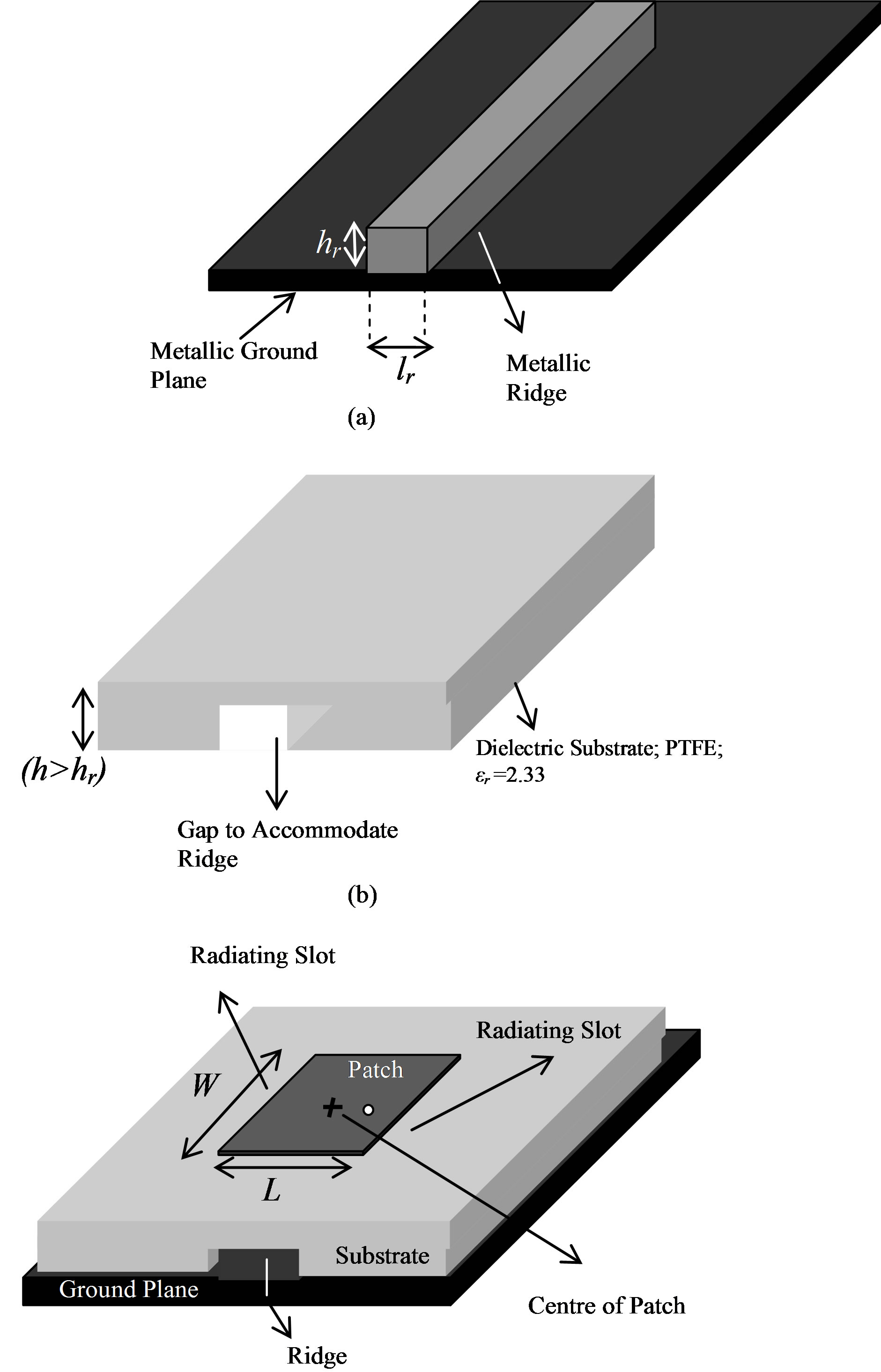
A rectangular microstrip antenna with length L = 12 mm and width W = 18 mm is shown in Figure 1 (top-view of the patch and side view of whole antenna structure). A dielectric substrate of thickness h = 1.575 mm and relative permittivity of εr = 2.33 is sandwiched between the patch and ground plane. Four slots of length Ls = Ws = 0.5 mm at four corners have been introduced to reduce cross polarized radiation. A metallic ridge of length lr = 5.5 mm and height hr = 1.5 mm is introduced on the
 (c)
(c)
Figure 1. Schematic diagram of the proposed antenna (a) Conventional ground plane with a ridge of height hr; (b) PTFE substrate of thickness (h with h > hr) with a gap to accommodate ridge; (c) Overall structure.
ground plane When this antenna is fed with coaxial probe at proper feed location (x′, y′), the structure becomes radiating. The ground plane dimension for the present investigation has been chosen to 1.5λ × 1.5λ.
3. Results and Discussions
Simulated results [12] obtained for the characteristics of the proposed antenna in its whole operating band.
Figure 2 shows the complete return loss profile of the conventional antenna and also compared with the proposed antenna. It shows that the conventional patch resonates at 7.23 GHz with an impedance bandwidth of 290 MHz i.e. in the range of 7.06 GHz to 7.35 GHz. But in case of proposed antenna it resonates at 11.07 GHz with an impedance bandwidth of 1170 MHz i.e. in the range of 10.62 GHz to 11.79 GHz. Thus it is clear from Figure 2 that the proposed antenna yields a fractional bandwidth of 11% where the conventional antenna using same patch dimension gives only 4%.
If we put a metallic ridge of length lr and height hr on the ground plane along the centre of the patch (along its width) as shown in Figure 1, then the resonant frequency of dominant TM10 is unaltered while that for second higher order mode TM20 decreases than its conventional value. As seen from Figure 2, the resonant frequency of dominant TM10 mode is 7.23 GHz. Thus, it is expected to get an another higher order mode TM20 nearly at 14 GHz. But in the proposed structure the higher order mode TM20 resonates at 10.5 GHz. This can be explained using transverse resonance method as follows:
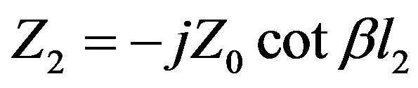
Resonant frequency of dominant TM10 mode is  and that for second higher order mode TM20 is
 .
.
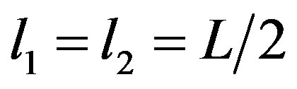
If we consider the two radiating slots of the patch as open circuit and at the same time the patch and ground plane constitute a parallel plate guide, then we can say two open circuited parallel plate guides of length l1 = l2 =
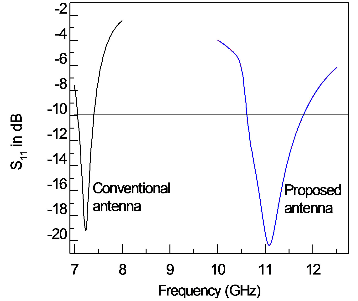
Figure 2. Return loss profile of the conventional antenna and the proposed structure.
L/2 are connected front to front along the centre of the patch. These parallel plate guides are producing input impedances of Z1 and Z2 which are parallel. At this region, a ridge of length lr and height hr exists on the ground plane which simulates capacitance Cp.
Thus,
 (1)
(1)
 (2)
(2)
As
 (3)
(3)
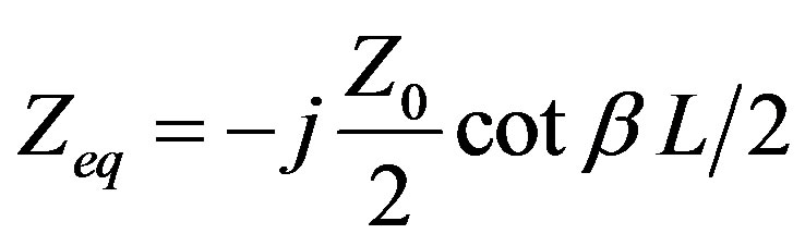
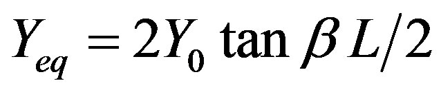
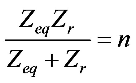
As two open circuited parallel plate guides of length l1 = l2 = L/2 are connected front to front in parallel, the equivalent input impedance Zeq can be written as
 (4)
(4)
capacitance produced by ridge is
 (5)
(5)
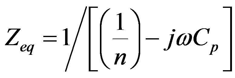
As the capacitance produced by ridge and the Zeq are in parallel,
 (6)
(6)
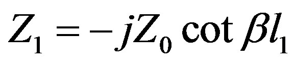
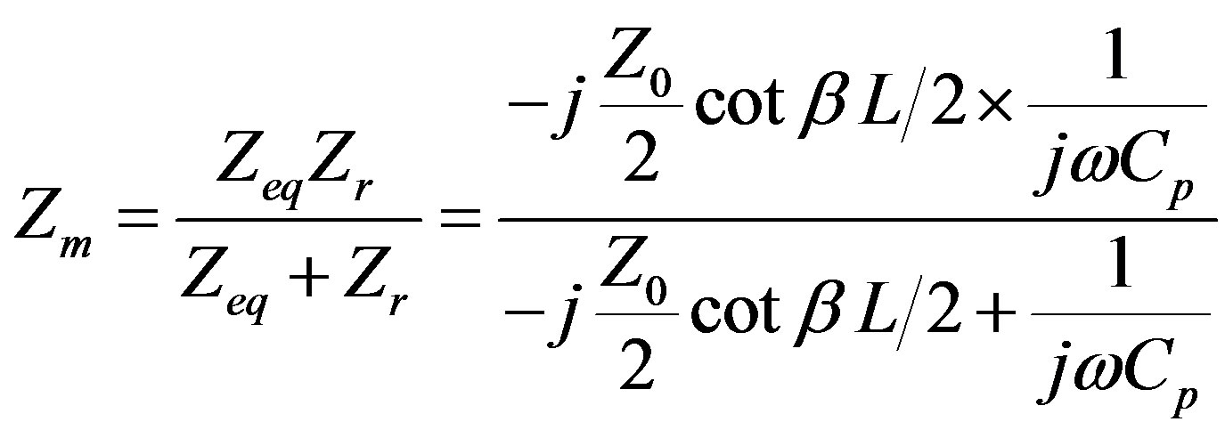
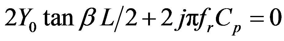
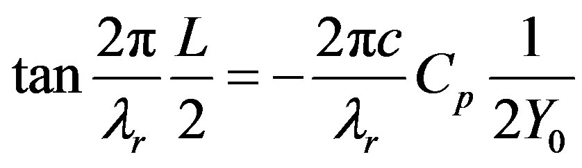
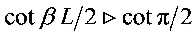
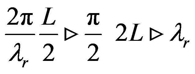
Using transverse resonance method, for dominant mode Zm to be zero and hence we can write:
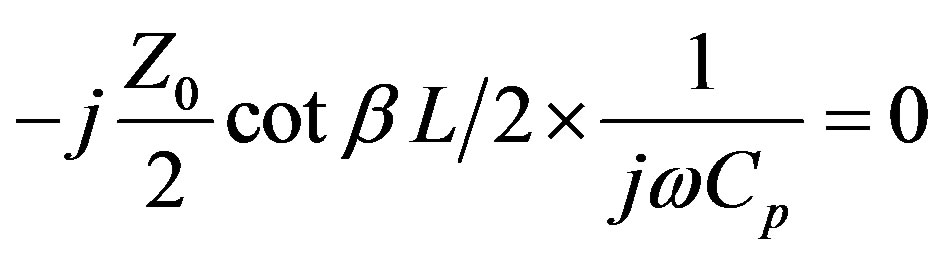 (7)
(7)
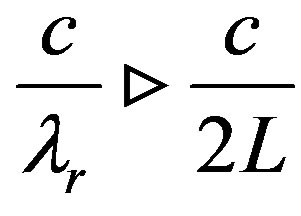
This leads to
 (8)
(8)
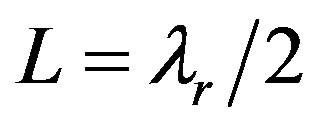
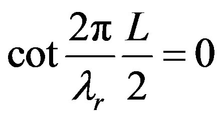
Thus the resonant frequency of dominant TM10 mode is 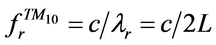 is kept unaltered.
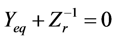
Now using transverse resonance method, for second higher order mode TM20; impedance at the centre is infinite which in other tern gives zero admittance.
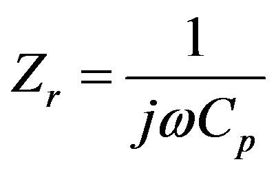
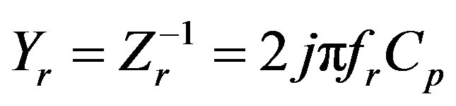
At centre the two open circuited parallel plate guide provides the equivalent admittance of Yeq and capacitance produced by ridge is Zr = 1/jωCp.
Thus, at central region of the patch, for second higher order mode TM20,
 (9)
(9)
 (10)
(10)
Admittance of capacitance Yr as:
 (11)
(11)
Thus,
 (12)
(12)
If no ridge is there then we may write Cp = 0; which gives
 (13)
(13)
 (14)
(14)
Thus,
 (15)
(15)
But if ridge is placed then capacitance will no longer be zero, Thus if,
 Negative finite value as in Equation (12)
 (16)
(16)
 (17)
(17)
 (18)
(18)
 (19)
(19)
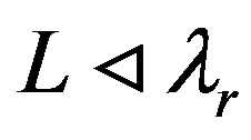
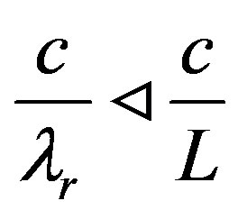
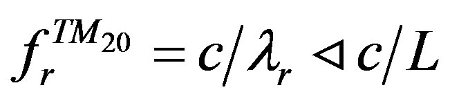
Which indicates that the resonant frequency of second higher order mode TM20  in case of the proposed structure is lesser than the resonant frequency (c/L) of that mode in conventional patch antenna.
Now, this theory is valid if we introduce a ridge of small length (lr), so that the capacitance developed by ridge is restricted to be along the central region (the region of zero impedance for dominant TM10 mode) under the patch. We know that the impedance of patch gradually increases as we move from centre of the patch towards its edge [13].
Now, as lr increases, the ridge is gradually extended towards the radiating slot means the edge of the patch. Thus the capacitance developed by ridge is moving towards the radiating slots where the impedance of the patch increases rather than being at zero value.
Thus using (4), (5), (6), (7) we may write,
 (20)
(20)
Thus,
 (21)
(21)
As ω is too large and n is also becoming large, so, 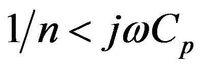 and thus the denominator is negative. This negative sign will be cancelled by the negative sign of left hand side as obtained from (4). Thus we may deal with the modulus values, hence
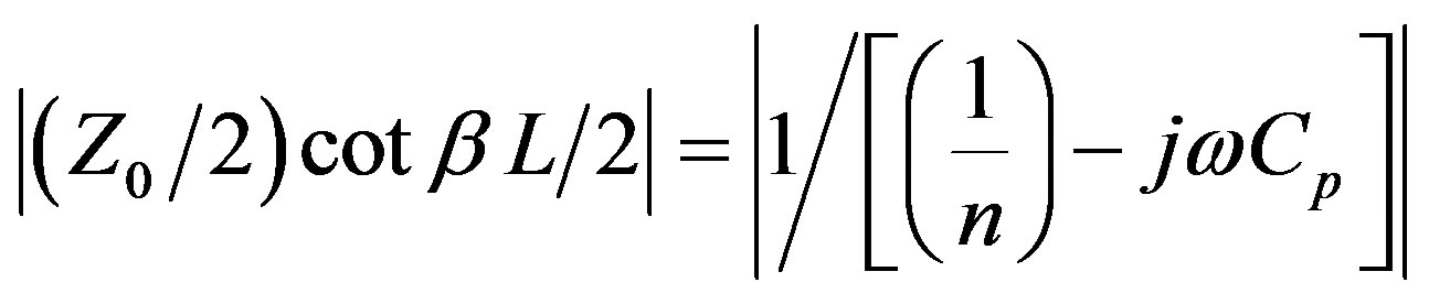 (22)
(22)
Actually, if the ridge size increases, the capacitive discontinuity produced below the patch decreases. In this way, when ridge becomes sufficiently large so that, it covers whole region below the patch, then the structure acts as a patch on thin substrate because the total ridge section will behave as truncated ground plane and the extra capacitance produced by ridge will be lost.
Close inspection of variation of 1/n with the distance from centre of the patch towards edge is smaller than the variation of Cp with the same as lr increases.
As lr increases, n increases which in turn increases 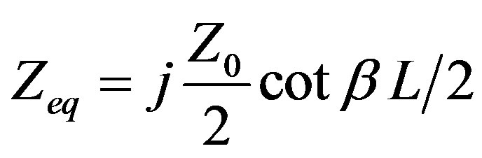 in positive side of the reactance curve.
Thus,
 (23)
(23)
 (24)
(24)
Hence,
 (25)
(25)
which indicates that the resonant frequency of dominant mode TM10  in case of the proposed structure is greater than the resonant frequency (c/2L) of the same dominant mode TM10 in conventional patch antenna.
This is clearly obtained from Figure 3 that, as we increase the value of lr, the resonant frequency of second higher order mode does not vary but that for 1st order dominant TM10 increases gradually. In this way, when the resonant frequency of dominant mode TM10 merges with of second higher order mode, the resultant return loss profile yields broader bandwidth (around 11%).
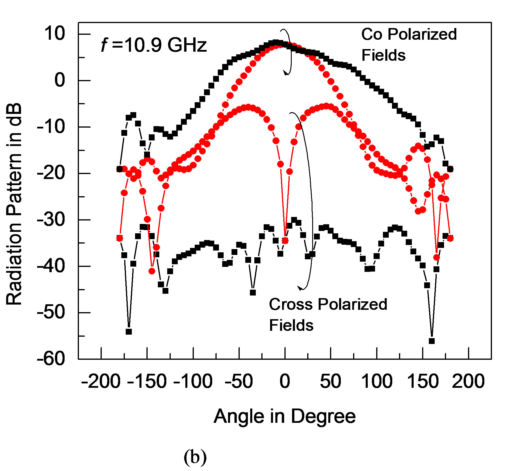
Figure 4 shows the radiation characteristics of the proposed antenna in the entire band of operation i.e. from 10.62 GHz to 11.79 GHz. It is found that the radiation characteristics over the entire band is similar except some changes in peak gain. It is also evident from the Figure 4(f) that, co-polar radiation characteristics is slightly degraded than others at higher side of the spectrum. It is
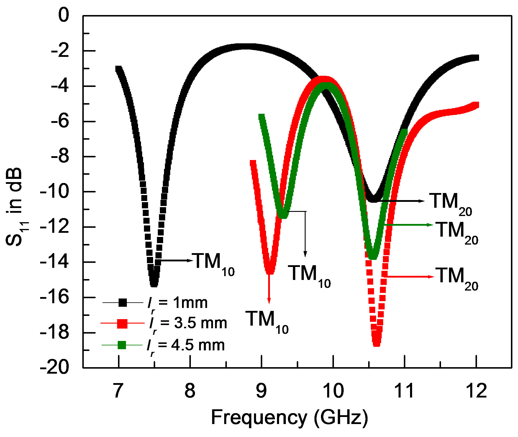
Figure 3. Return loss profile for dominant TM10 and second higher order mode TM20 for proposed antenna for different values of lr.
 (c)
(c)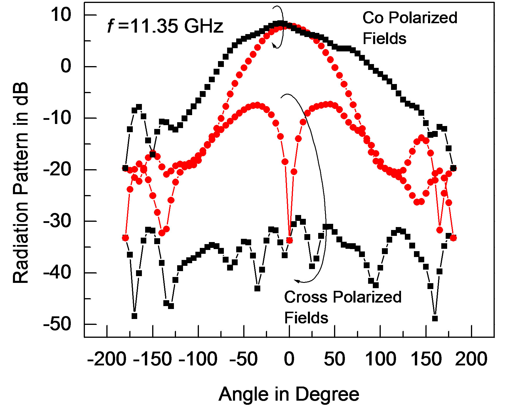 (d)
(d)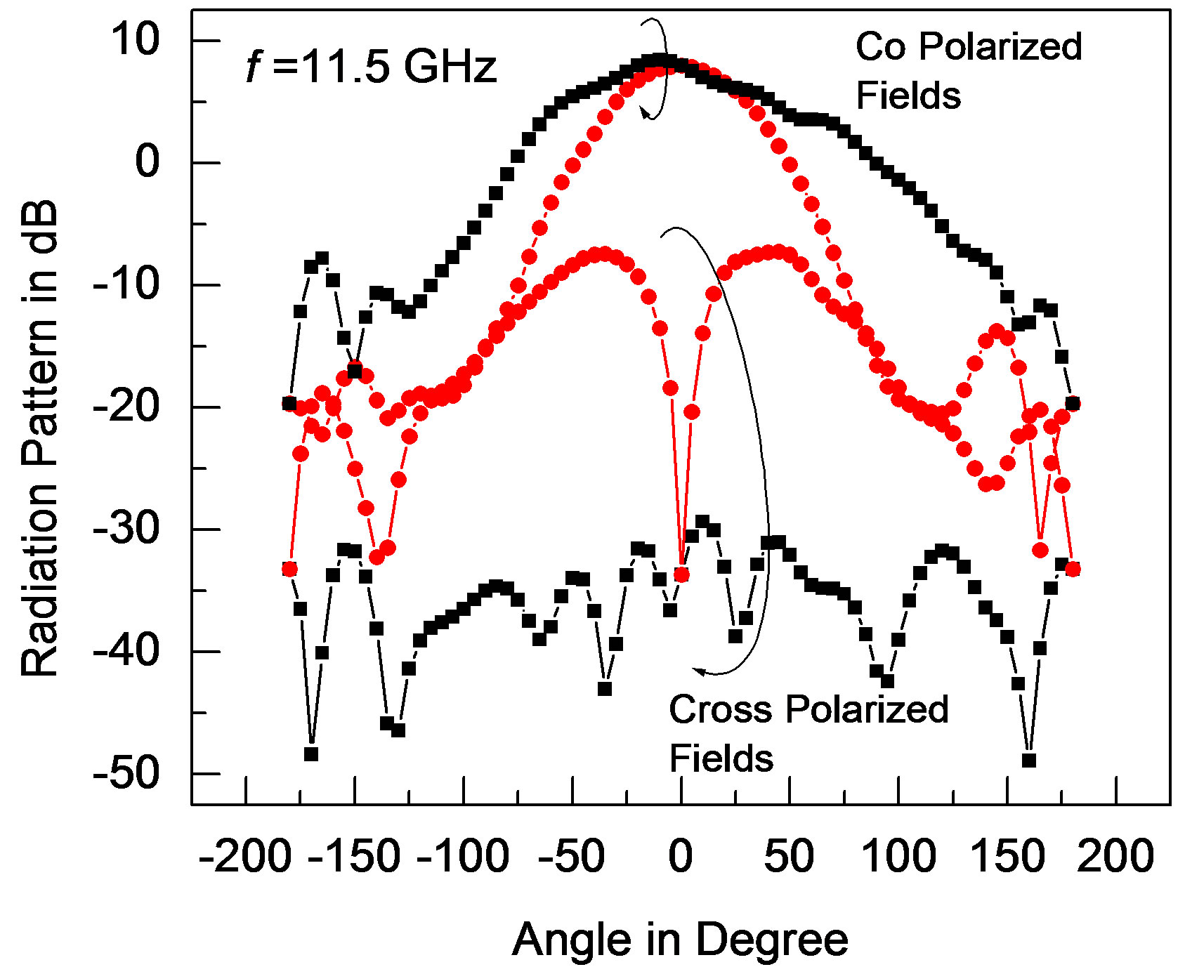 (e)
(e)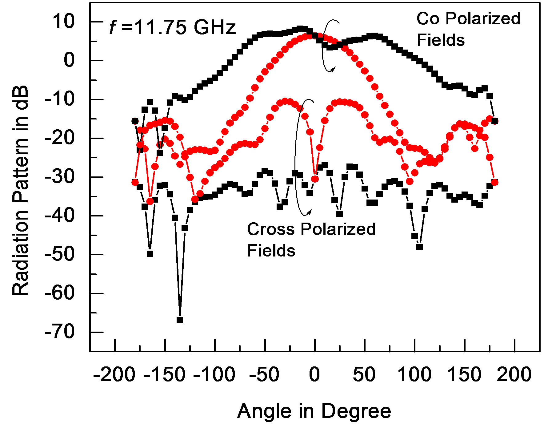 (f)
(f)
Figure 4. Radiation characteristics of the proposed antenna at different frequencies over its operating band.
expected, as we have seen that there is inclusion of TM20 mode with TM10 band; in the higher range of the band the characteristic of TM20 becomes predominant. However, this distortion at frequency 11.75 GHz is quite small as obtained from the same Figure 4(f). Thus, the proposed antenna possesses the pattern bandwidth of 11%.
The variation of the peak gain as a function of frequency is shown in Figure 5. The maximum peak gain for the proposed structure is obtained at frequency 11.35 GHz as is clear from Figure 5. The peak gain variation in the whole operating band of this proposed antenna is very small (nearly 0.6 dBi) i.e. from 7.42 dBi to 8 dBi.
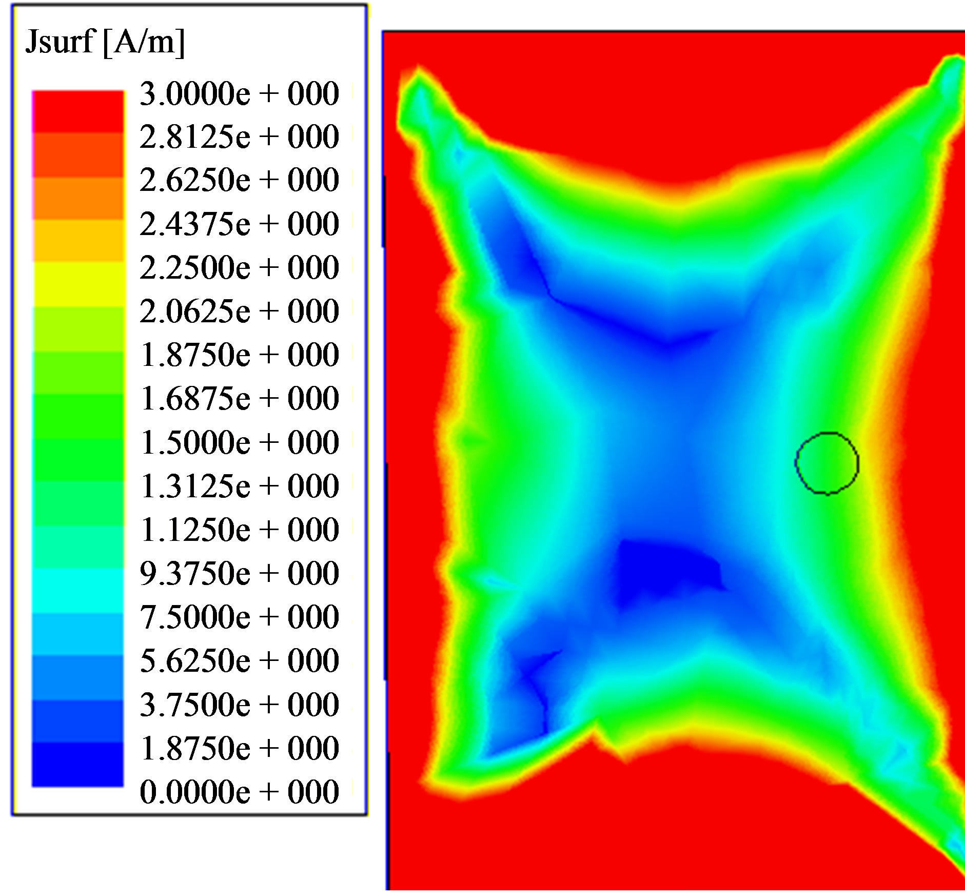
The magnitude of the electric field distribution over the patch is shown in Figure 6. The electric field distribution over the patch is quite different from that at conventional patch antenna. Actually the assimilation of two modes beneath the patch may be attributed for this difference in electric field distribution over the patch.
4. Conclusion
A single layer, single element broad band microstrip antenna is proposed and verified its behavior quantitatively.
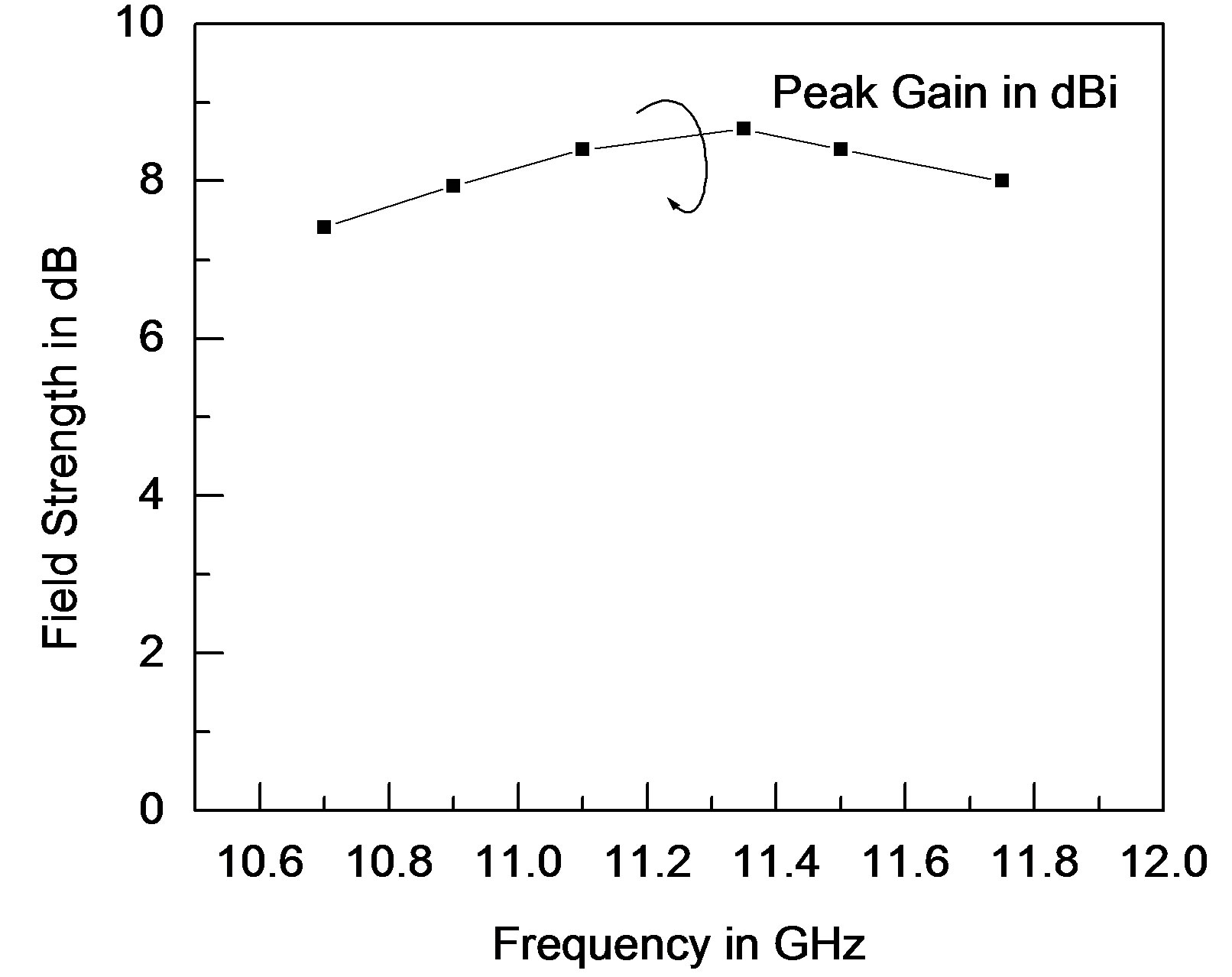
Figure 5. Variation of peak gain of the proposed antenna in its operating band.
 (a)
(a)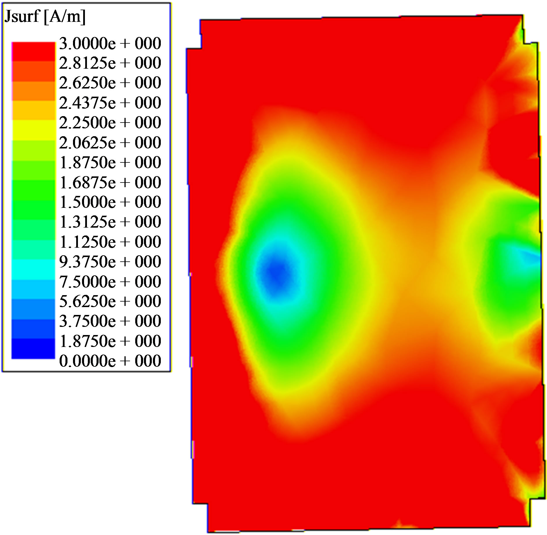 (b)
(b)
Figure 6. Magnitude of electric fields distributed over the patch. (a) Conventional antenna; (b) Proposed antenna.
Concrete physical insight using transverse resonance method is explained for proposed structure which will help the scientist, research community and practicing engineers to design and develop microstrips antenna with broader bandwidth. The proposed antenna is very simple and cost effective as no modification is there except a metallic block (ridge) at ground plane. The proposed antenna is having nearly constant radiation pattern and peak gain throughout its operating band. The study of detail variations of second order resonant frequencies as a function of ridge size is very helpful for future investigations.
REFERENCES
- G. Kumar and K. P. Ray, “Broadband Microstrip Antennas,” Artech House, Norwood, 2003.
- M. R. Solanki, K. Usha Kiran and K. J. Vinoy, “Broadband Design of a Triangular Microstrip Antenna with a Small Capacitive Feed,” Journal of Microwaves, Optoelectronics and Electromagnetic Applications, Vol. 7, No. 1, 2008, pp. 44-53.
- L. C. Ping, C. K. Chakrabarty and R. A. Khan, “Design of Ultra Wideband Slotted Microstrip Patch Antenna,” 2009 IEEE 9th Malaysia International Conference on Communications (MICC), 15-17 December 2009, pp. 41-45.
- Y. Ge, K. P. Essele and T. S. Bird, “A Broadband EShaped Patch Antenna with a Microstrip Feed,” Microwave and Optical Technology Letters, Vol. 42, No. 2, 2004, pp. 111-112.
- G. Mayhew-Ridgers, J. W. Odendaal and J. Joubert, “Single Layer Capacitive Feed for Wideband Probe-Fed Microstrip Antenna Elements,” IEEE Transactions on Antennas and Propagation, Vol. 51, No. 6, 2003, pp. 1405-1407. doi:10.1109/TAP.2003.812186
- A. A. Eldek, A. Z. Elsherbeni and C. E. Smith, “Characteristics of BOW-TIE Slot Antenna with Tapered Tuning Stubs for Wideband Operation,” Process in Electromagnetics Research, Vol. 49, 2004, pp. 53-69. doi:10.2528/PIER04021301
- K. L. Wong and Y. F. Lin, “Microstrip-Line-Fed Compact Broadband Circular Microstrip Antenna with Chip Resistor Loading,” Microwave and Optical Technology Letters, Vol. 17, No. 1, 1998, pp. 53-55. doi:10.1002/(SICI)1098-2760(199801)17:1<53::AID-MOP14>3.0.CO;2-C
- R. B Waterhouse, “Broadband Stacked Shorted Patch,” Electronic Letters, Vol. 35, 1999, pp. 98-100. doi:10.1049/el:19990086
- D. M. Pozzar, “Microstrip Antenna Coupled to Microstripline,” Electronic Letters, Vol. 21, No. 2, 1995, pp. 49-50.
- A. Kaya, “High Gain Rectangular Broad Band Microstrip Antenna with Embeded Negative Capacitor and Chip Resistor,” Progress in Electromagnetics Research, Vol. 78, 2008, pp. 421-436. doi:10.2528/PIER07100202
- V. Tarange, T. Gite, P. Musale, S. V. Khobragade and V. R. Anitha, “A Broadband Design of H-Shaped Microstrip Antenna with Capacitive Feeding,” XXX URSI General Assembly and Scientific Symposium of International Union of Radio Science, (978-1-4244-5118-0/11), Istanbul, 13-20 August 2011.
- HFSS: High Frequency Structure Simulator, v.10, Ansoft Corp.
- S. Chattopadhyay, M. Biswas, J. Y. Siddiqui and D. Guha, “Input Impedance of Probe-Fed Rectangular Microstrip Antennas with Variable Air-Gap and Varying Aspect Ratio,” IET Microwaves, Antennas and Propagation, Vol. 3, No. 8, 2009, pp. 1151-1156. doi:10.1049/iet-map.2008.0320