Journal of Electromagnetic Analysis and Applications
Vol.4 No.3(2012), Article ID:18241,11 pages DOI:10.4236/jemaa.2012.43016
Periodic Planar Multilayered Substrates Analysis Using Wave Concept Iterative Process
![]()
1Laboratoire d’Electronique, Departement de Physique, Faculte des Sceinces de Tunis, Tunis, Tunisie; 2Laboratoire d’Electronique, Departement de Physique, Faculte des Sceinces de Tunis, Tunis, Tunisie; 3Laboratoire d’Electronique, Groupe Microonde ENSEEIHT, Toulouse, France.
Email: hajlamjed@yahoo.fr
Received January 1st, 2012; revised February 5th, 2012; accepted February 13th, 2012
Keywords: WCIP; Transmission Line Theory; Patch Antenna; Frequency Selective Surfaces (FSS)
ABSTRACT
Due to the practical importance and difficulties associated with their closed form solutions, the experimental and computational study of periodic planar multilayered structures, such as FSS in multilayered configuration and Multilayered Planar antennas array, are in complementary progress. During the past two decades, the widespread use of such methods has allowed a broad range of important scattering problems involving non-standard shapes, boundary conditions and material composition to be solved. In this sense, an efficient iterative technique based on the concept of wave is presented for computing periodic substrates in multilayered configuration. This paper presents an extensible approach of the iterative method to study multilayered substrates (n layers in which n = 2, 20) with spatial periodicity in multilayer configuration. Our new approach is performed in order to study 3 dimensional structures by the method called Wave Concept Iterative Process (WCIP). This method is adapted in its original form to study 2 dimensional structures. The third dimension is modulated by transmission line as an approximation for every mode in spectral domain. The utility of the new WCIP appears because of its fast convergence and little consumption in memory.
1. Introduction
Periodic structures have a variety of important applications in electromagnetic engineering and modern technologies. Commonly used, periodic structures include frequency selective surfaces, optical gratings, phased array antennas and various metamaterials. Both applications can essentially be formulated as planar multilayered periodic arrays of metallic patches and/or slots. The use of periodic conditions to model the behavior of these arrays is justified by their large size (typically, 100 * 100 elements). As a result, the development of fast and efficient software tools, that can accurately predict the electrical behavior of the component being investigated, is of fundamental importance. For mechanical reasons, or the purposes of reducing the angular sensitivity [1], FSS structures are often mounted on dielectric substrates. Now more complex mediums have been used as the substrates: some works were reported on FSS structures with ferrite substrates [2] and with chiral substrates [3,4].
In this paper, to reduce the computational effort required for the analysis of arbitrary microwave components, we suggest an efficient method which can be incorporated in a circuit simulator. This theory is an extension of previous studies investigated with the MLC-WCIP [5], but here we introduce a new parameter characterized by the introduction of periodicity as a new approach in the studied structures (new boundaries conditions). The importance of periodicity, as a new investigation, appears in complex periodic multilayered structures characterized by infinite geometric dimension. A new approach is necessary to study the entire structure because of its infinite geometric dimensions. The idea is to extract and study one multilayered cell to conclude about the entire structure with its infinite cells.
This approach consists in introducing periodic walls for the analyzed substrate characterized by periodic elements and changing Fast Modal Transformation (FMT) of selected cells by new equivalent FMT taking account the presence of periodic lateral walls of the selected substrate. It offers high spatial resolution with low computing resources in time and memory, and makes the iterative method more effective in modeling arbitrarilyshaped structures.
Here, we have achieved a factor of 4 in memory reduction and 7 - 11 in CPU speedup over other method (here is finite element method (F.E.M.) in case of typical meshing.
2. Theory
2.1. Iterative Method
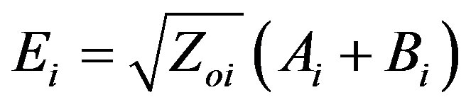
The basis analysis of microwave structures with our electromagnetic method called wave concept iterative method (WCIP) has been described in [5]. It is based on the Wave Concept, which is introduced by writing the tangential (plane Ω) electric and magnetic fields, in terms of terms of incident (A) and reflected (B) waves (Figure 1). It leads to the following set of equations:
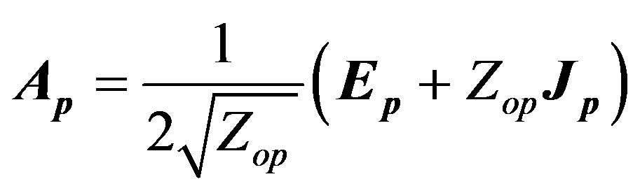 (1)
(1)
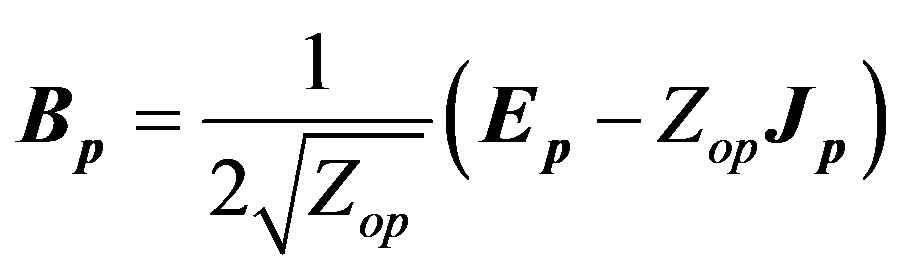 (2)
(2)
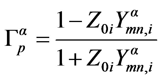
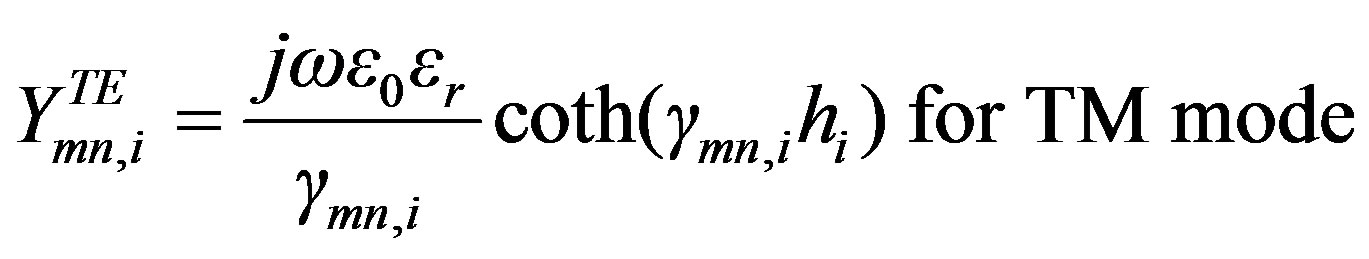
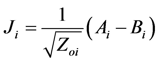
where Zop is the characteristic impedance of the medium p given by
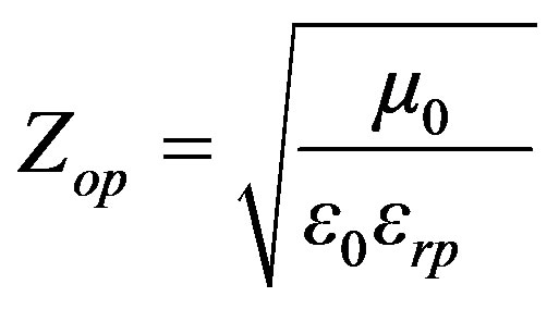 (3)
(3)
Two operators are successively applied to these waves:
The scattering operator  [6], which takes into account the boundary conditions in the spatial domain
  and
and  on the dielectric,
  on the metal and finally
 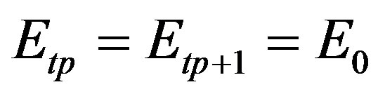 on the source) is expressed as follows Equation (4):
where Hm = 1 on the metal and 0 elsewhere.
Hd = 1 on the dielectric and 0 elsewhere.
Hs = 1 on the source and 0 elsewhere.
and Z0 is the admittance in the source zone.
Zo,p is the characteristic impedance of the layer p.
 (4)
(4)
The incident waves are reflected on the upper and lower parts of the metallic box. Consequently, the relationship between waves in spectral domain is:
 (5)
(5)
where the reflection operator , which takes into account the environment’s reaction in the spectral domain, is defined as:
 (6)
(6)
This operator depends hugely on the mode nature and the used waveguide. Here, we express 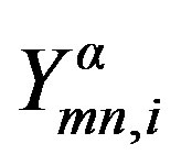 that depends of these two factors.
• In case of open waveguide.
ü 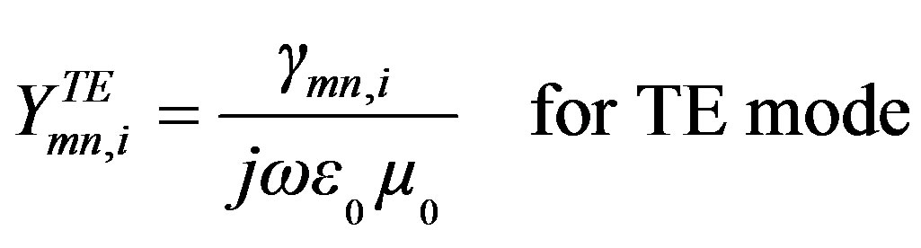
• 
• In case of Short-circuited waveguide with ground plane.
ü 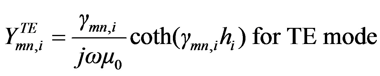
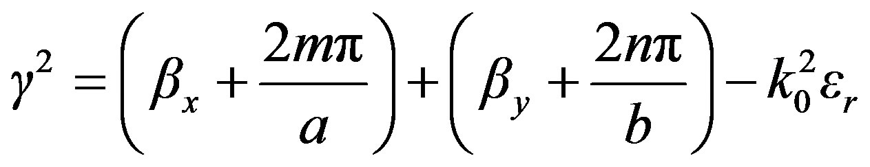
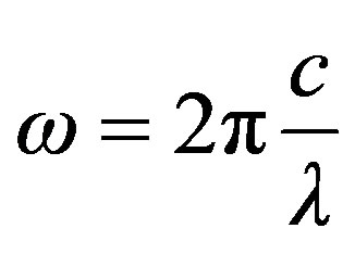
where 
 is the wave number in the free space.
The implementation of the iterative process consists of establishing a recursive relationship between the waves in the two regions 1 and 2, using the reflection operator in the spectral domain and the boundary conditions required on the interface plane Ω (Figure 1).
The FFT-2D in wave guide environment known as fast modal transformation (FMT) [5] is used to pass from spatial domain to spectral domain and vice versa.
The definition of the Fast Fourier transformation (F.F.T-2D) in waveguide environment is as Equation (7):
 (7)
(7)
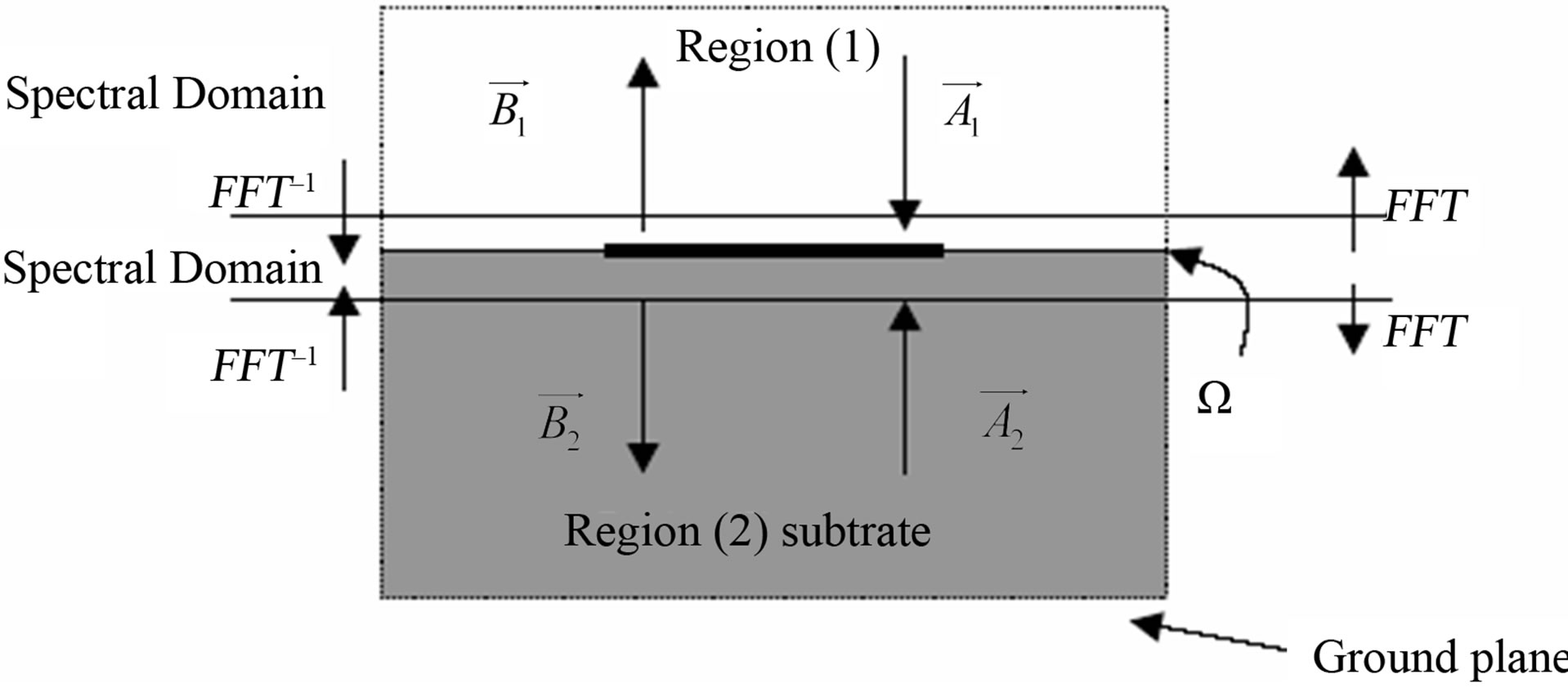
Figure 1. Iterative process.
Cosin and Sincos represent the development of the FFT under shape of sines and cosines with

A successive set of iterations is considered to determine a relationship between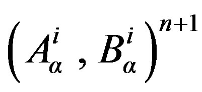 ,
,  corresponding to the
  and n iteration. A schematic description of the iterative technique is illustrated in Figure 2.
This algorithm requires the meshing of the interface surface into small rectangular sub-domains. So the metallic, dielectric and source domains are characterized by the corresponding matrix Hm, Hd and Hs. The domain matrix elements take the value 1 in the corresponding cells and zero elsewhere. However, we can express the boundary conditions in terms of waves on each cell.
 (8)
(8)
 (9)
(9)
Finally, it’s possible to determine the admittance matrix, from that, the scattering matrix Sij for a two port can be obtained by the following equation:
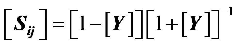 (10)
(10)
[Y] is the admittance matrix.
2.2. Formulation of Wave Concept Iterative Process for the Analysis of Periodic Planar Multilayer Substrates
To study multilayered periodic structures, we have to present the Wave Concept Iterative Method in another new formulation taking account the presence of different domains (metallic and dielectric) in each interface and we have to present the relationship between them by taking account possible electrical equivalent scheme.
where:
(A, B) are the waves into their established spectral and spatial forms.
Q: a quadruple in spectral domain defined by the transmission line Theory [5]. This equation will present
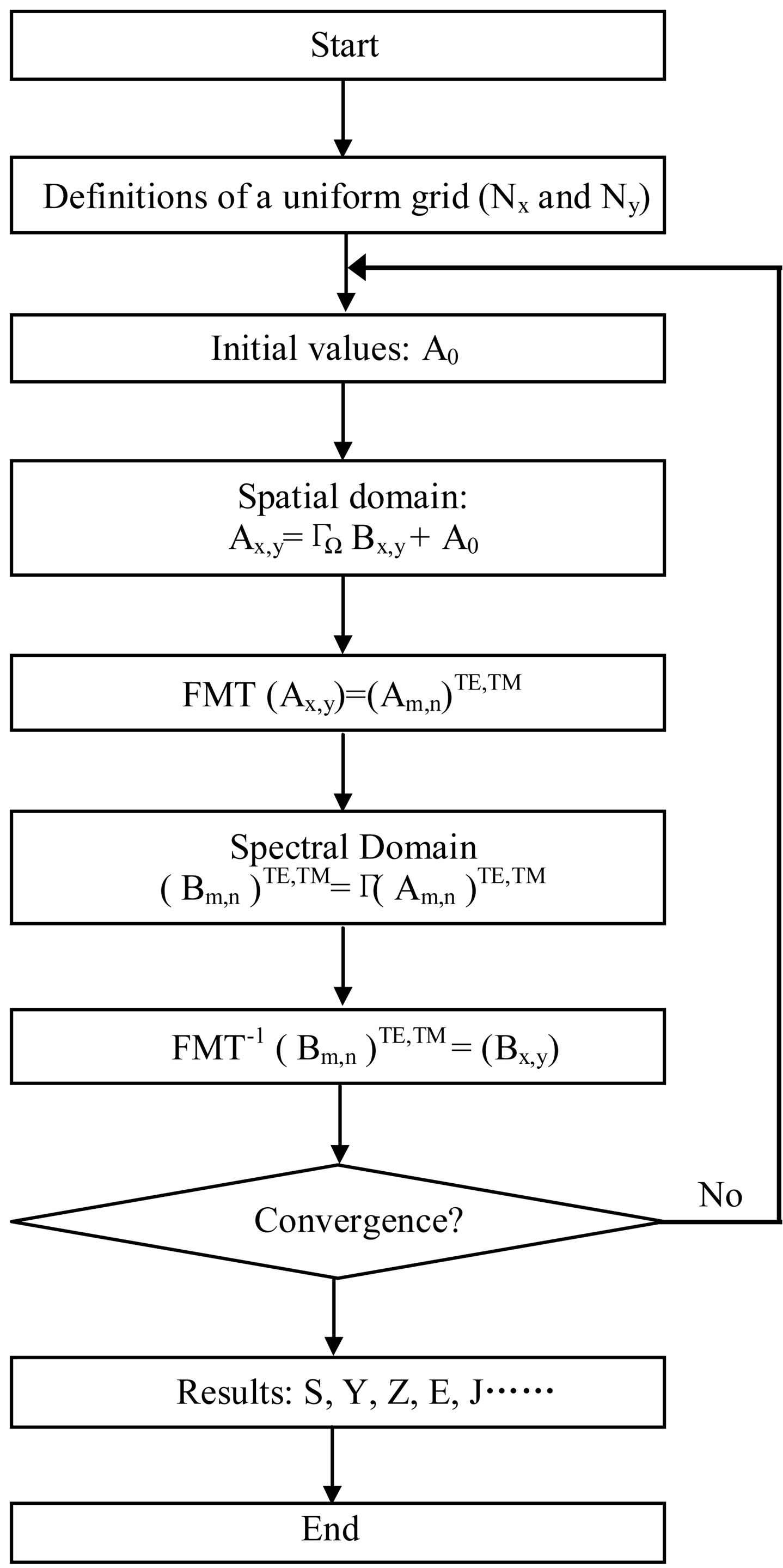
Figure 2. Iterative process algorithm.
the relationship between transmitted and reflected waves in spectral domain.
The multilayered structures (Figures 3 & 4) needs another formulation of the iterative method based on multilayered contribution of Wave Concept Iterative Process [5] taking into account the presence of middle which is represented by the scattering matrix and the down surface considered as a ground. The layer hn takes an important value because it designs the lower cover of the metallic box.
The periodic structures are characterized by their big sizes. The description of these structures in the space field requires a very large number of pixels, which is translated into a very high computing time and a very significant storage capacity. To simplify problem, we can benefit from the periodicity, by studying only one basic cell with one layer in a wave guide with periodic walls [7] and extend the theory to multilayered periodic structures including more complexity in its modelling.
Problems of corners are not treated because of the infinite dimension of different studied structures. Periodicity of these structures allows us to study only one motif. However, modification in lateral walls analysis will be
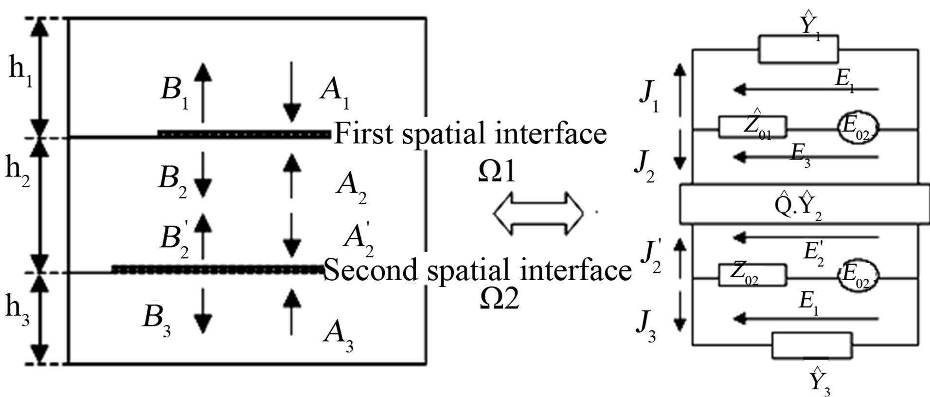
Figure 3. Double layered structure and its equivalent electrical circuit.

Figure 4. Multilayered structure and its equivalent electrical circuit.
necessary. New computation of Fast Fourier Transformation called Fast Modal Transformation (FMT) will be necessary to analyze periodic structures.
Figure 5 illustrates a Periodic Planar multilayer structure with n layers where θ and φ represent incident angle.
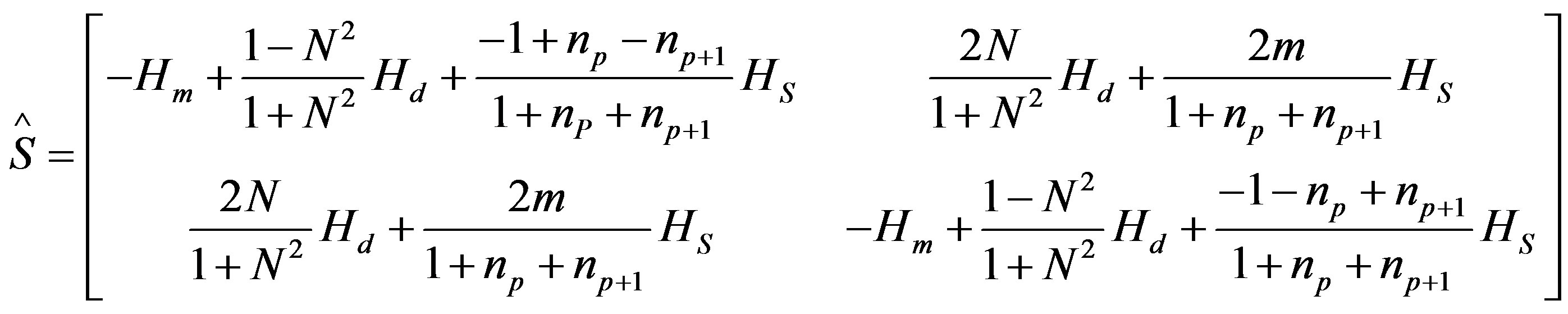
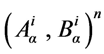
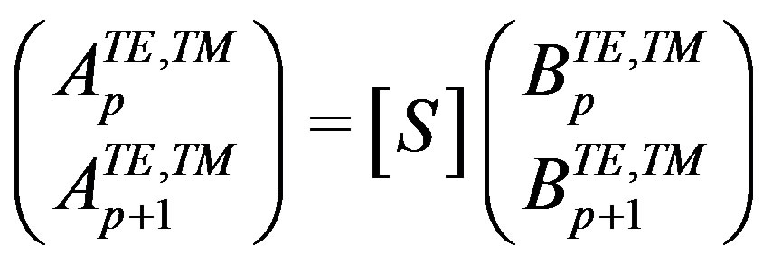
In periodic contribution, the relationship between the waves (Ap, Bp) and (Ap+1, Bp+1) in each layer in spatial domain is:
• In middle interfaces p where 1 < p < n.
 (11)
(11)
 (12)
(12)
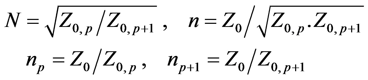
where

Z0 is the admittance in the source zone.
Zo,p is the characteristic impedance of the layer p.
and:
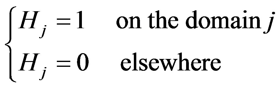
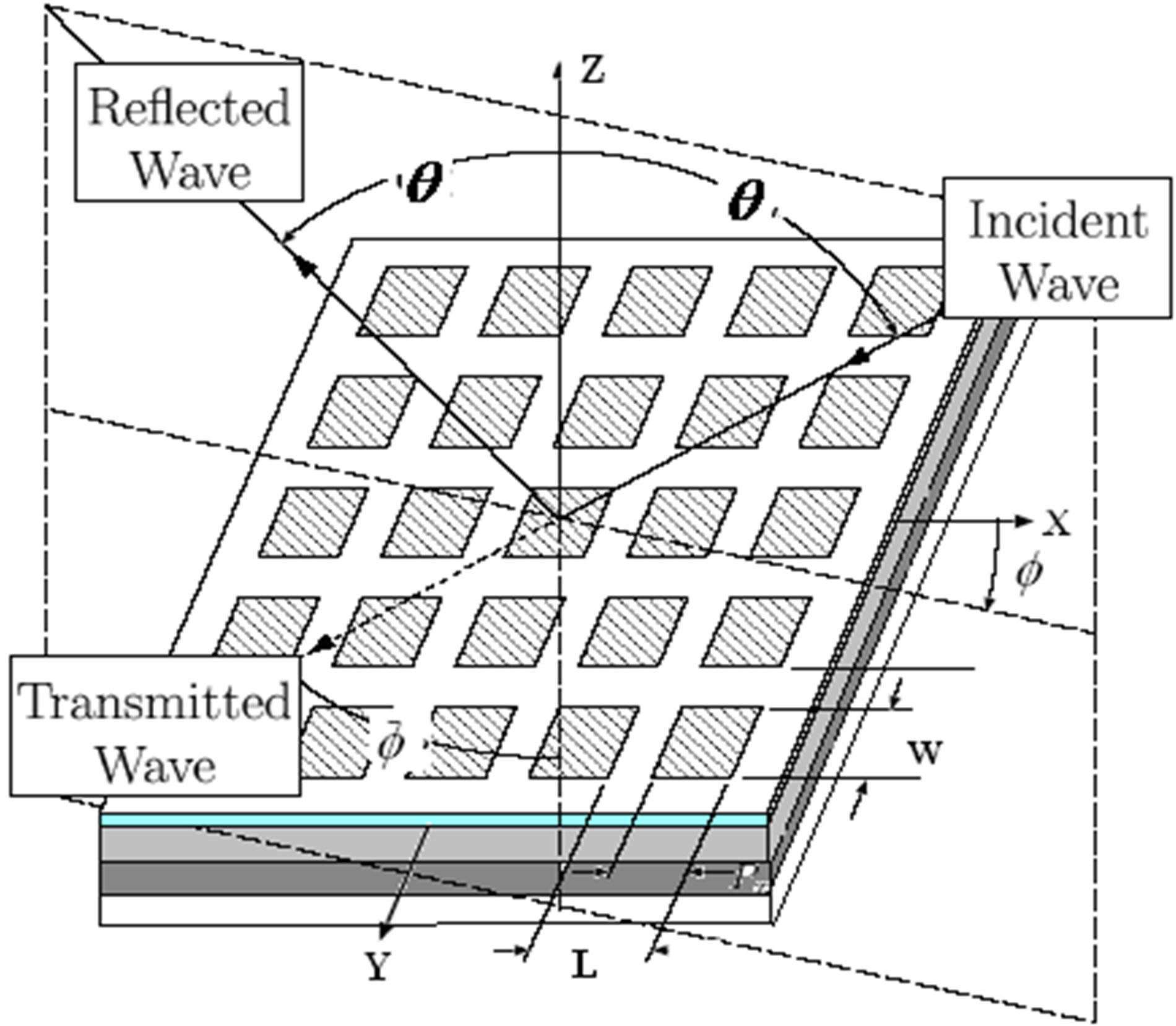
Figure 5. Periodic Planar multilayer structure with n layers where θ and φ represent the incident direction.
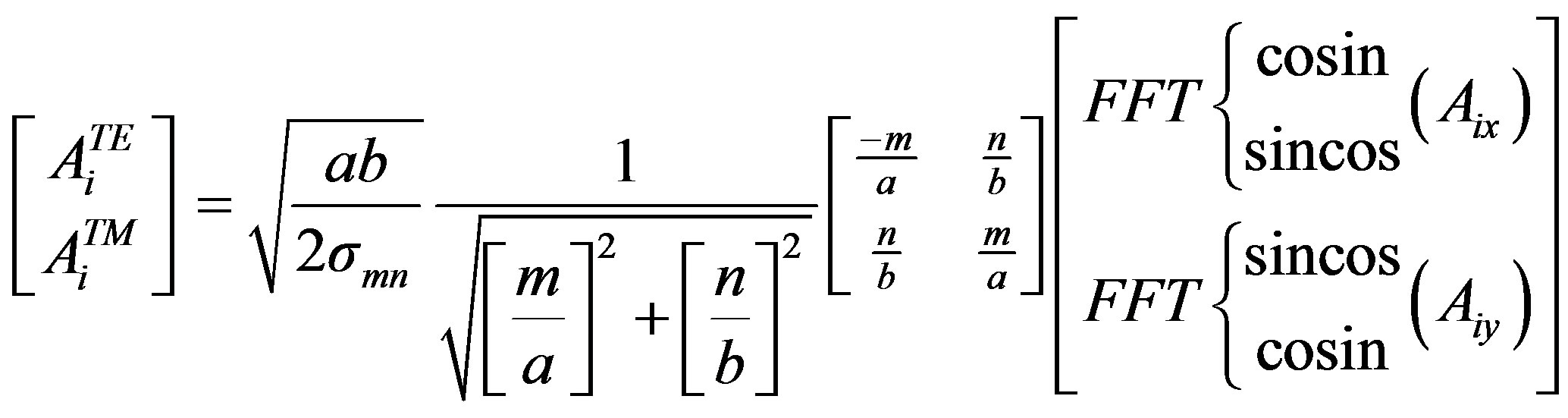
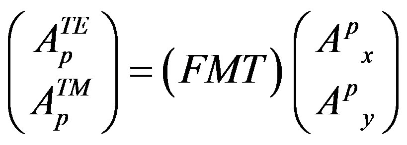
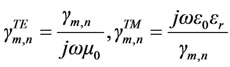
For periodic structures, the generating functions of the modes are exponential type.
By consequence the amplitudes of the modes are defined by projecting the coefficients of Fourier of the components of the electric field on the basis of mode (Transverse Electric: TE—Transverse Magnetic: TM).
Then, for TE mode equation begins:
 (13)
(13)
For TM mode equation begins:
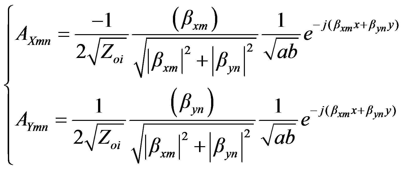 (14)
(14)
where
 (15)
(15)
and 
 : Wavelength in free space
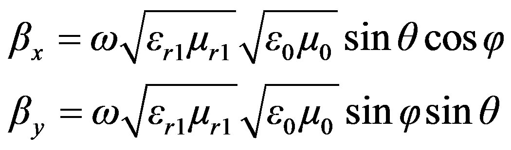
 Angles characterizing direction of incident plane wave.
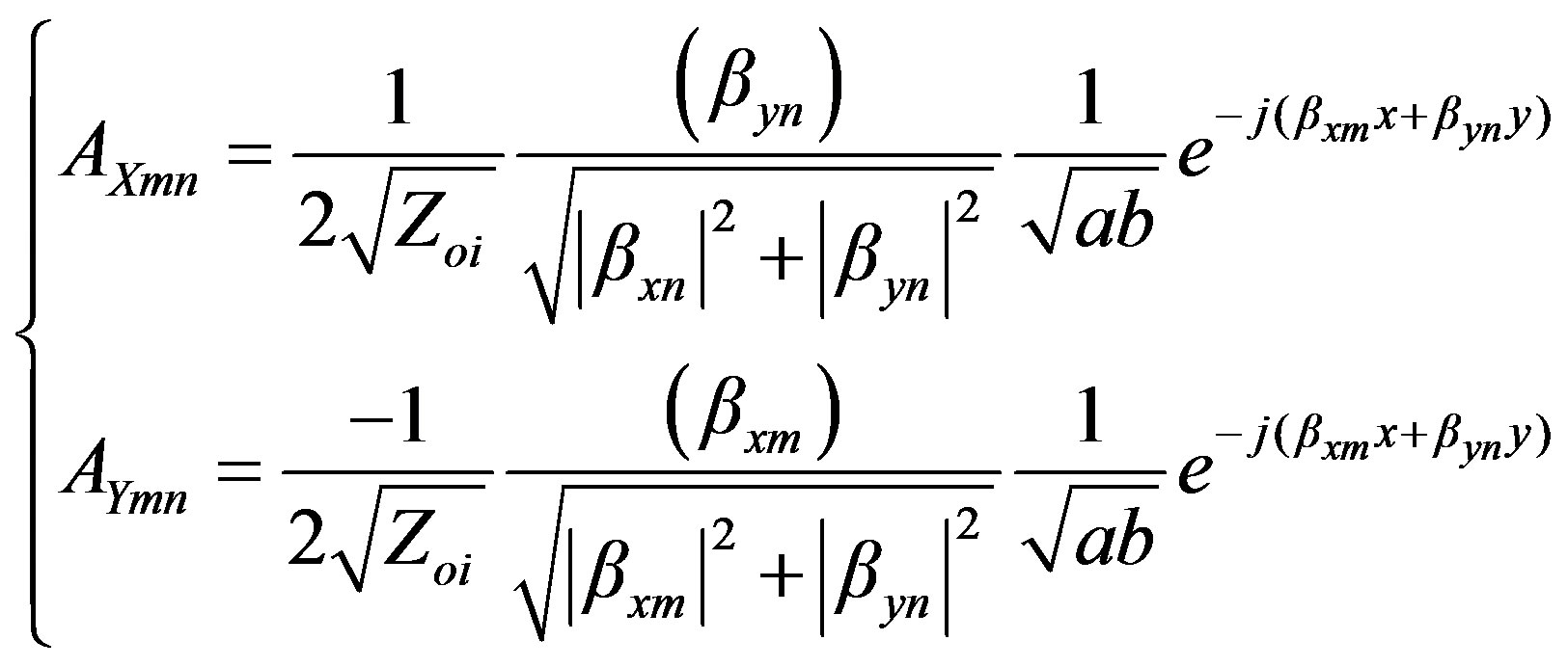
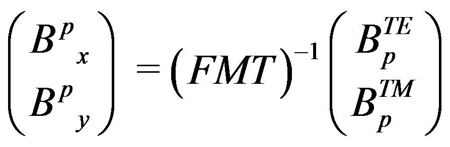
In our case, we try to develop a three dimensional case; that how we need a solution to pass from the down basis cell to the upper one. This passage between the spatial domain and the spectral domain is obtained by a periodic 2D Fast Fourier Transform (2D-FFT) (also called Fast Modal Transform FMT) in its periodic form. In this sense, a simplification is necessary because our method, in its basis formulation, is 2-dimensioal method. Consequently, the waves in spatial domain  have the expression in spectral domain:
 (16)
(16)
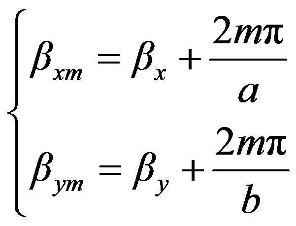
Here, we notice that (m, n) means the number of cells in spatial domain, but (p) the current number of layer which is included between 1 ≤ p ≤ n and n is the total number of layers.
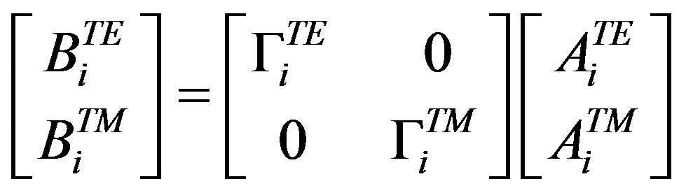
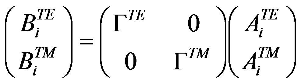
The concept of wave permits to deduce a spectral operator, connecting waves A with the waves B, the relations in the spectral field are given by the following system:
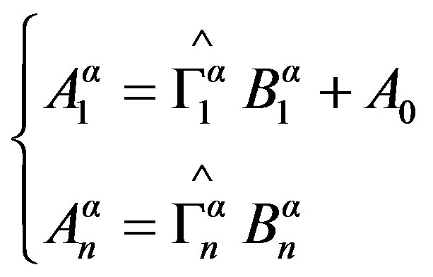 (17)
(17)
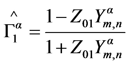 : Reflection coefficient in layer 1.
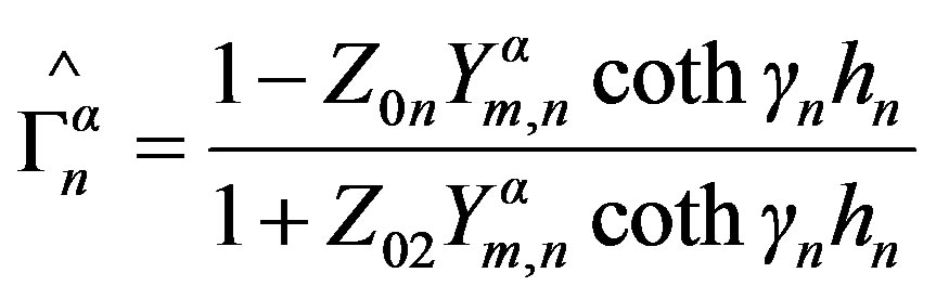 Reflection coefficient in layer n if this latter is limited by ground plane.
where
 (18)
(18)
 ,
,
The passage between 2 adjacent layers in spectral domain of a multilayered structure needs new formulation of relationship between waves (Ap, Bp) and (Ap+1, Bp+1)
in adjacent middle layers.
Consequently, for 2 ≤ p < n – 1, the relationship between the waves (Ap, Bp) and (Ap+1, Bp+1) is determined by using the transmission line theory [5].
Consequently, the scattering matrix of the transmission line is given by Equation (19).
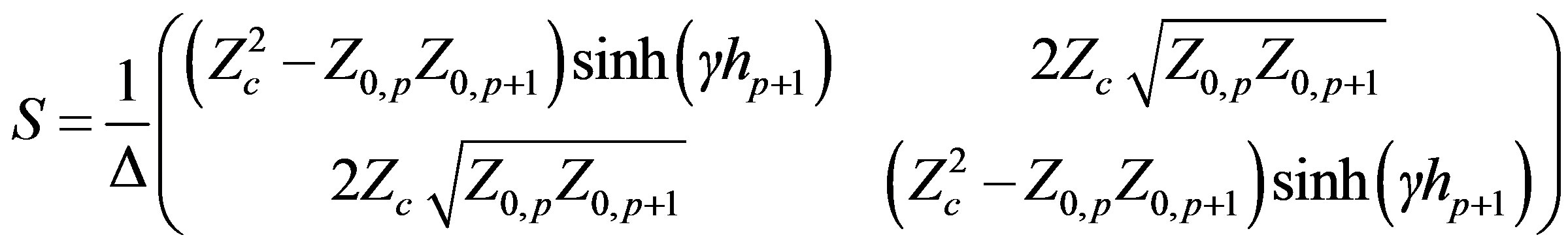 (19)
(19)
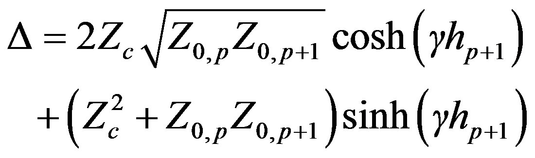
The relationship between waves in spectral domain in middle interfaces is summarized by the following equation:
 (20)
(20)
The passage between spectral domain and spatial domain is assured by the inverse 2D-FFT (FMT) taking account periodic configuration of lateral layers. Consequently, we have:
 (21)
(21)
Moreover, the reflected waves generated by the upper and lower covers of metallic box calculated by the reflection coefficient in the spectral domain are:
 (22)
(22)
where i = 1, or n.
In conclusion to this development, we have tried to reduce our work in one of the two TE or TM wave components because in case of existence of both, the problem will be more complicated.
Figure 6 presents a schematic description which summarizes the main operation of the periodic iterative procedure in a multilayer contribution.
The implementation of the iterative method consists of establishing a recursive relationship between waves at the k and k – 1 iteration, it is possible to determine the electric field and the current density at the air dielectric interface (plane p). After, that it is easy to deduce the expression of admittance matrix and reflection and transmission coefficients [8].
Also, we have to notify that convergence means stability of current density and electric field in each cell of each layer of our structure.
In the aim to present the efficiency of our method, we present the analysis of the Figure 7 in comparison with the F.E.M. method in case of adopting typical meshing of the 2-layered structure. This structure presents double
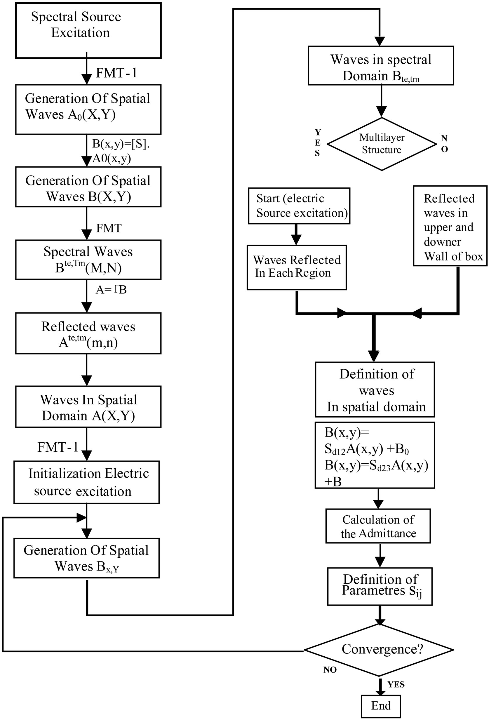
Figure 6. Schematic description of the periodic iterative procedure in multilayer contribution.
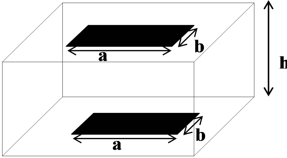
Figure 7. Rectangular two layered structure.
layered figure with different geometric parameters in case of maintaining the same distance between upper and down layers taking account necessity of coupling between them (distance between the 2 interface h = 2 cm).
The next table (Table 1) presents the efficiency of our method, in comparison with finite element method, Here, we present the gain obtained in time considering proper characteristics of the used machine for different size matrix with a CPU = 3 GHz and 4 Go of memory.
This purpose is greatly in accordance with our presentation of the method so called WCIP what is clearly about 7 times faster because of its formulation based on a 2 dimension strategy and taking the third one as a relationship between 2 different cells and relying them with the transmission line theory. Hence the F.E.M. is a 3- dimensional method.
That’s why our purpose will simplify the electromagnetic analysis of the CPU time of simulation.
3. Applications
3.1. Application 1: Analysis of Rectangular FSS of Repeated Structure
The PMC-WCIP is used to analyze the rectangular FSS of a repeated structure shown in Figure 8. It illustrates the grating of conducting plates, in the particular case of rectangular plates.
The structure consists of four layers in which the first and the last are air. Figure 9 represents the reflected power obtained by WCIP when normal incidence (θ and φ are equal to Zero) is considered. A grid of 64 by 64 pixels is used to define the interface and the results are recorded after 600 iterations. Resonance occurs at about 17.3 GHz.
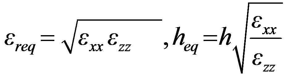
The anisotropy of the layers is taken into account in the analysis by the determination of the equivalent relative isotropic layers. When εxx = εyy, the parameters of this equivalent isotropic layer are given by [9] where h is the thickness of the anisotropic substrate.
Results are compared with experimental ones and they show good agreement [10]. Different geometric parameters are presented in Figure 8 that illustrates the Variation of the transmission power versus frequency, a = b = 1 cm, w = 0.0625 cm, L = 0.6875 cm, h1 = h2 = 0.05cm, εr1 = 2, εr2 = 1.
With modification of geometric parameters as follow: a = b = 1.8 cm, w = 0.6 cm, L = 1.2 cm, h1 = h2 = 0.15 cm, εr1 = εr2 = 4.4, Transmission and reflected power versus frequency are presented in Figures 10 and 11.
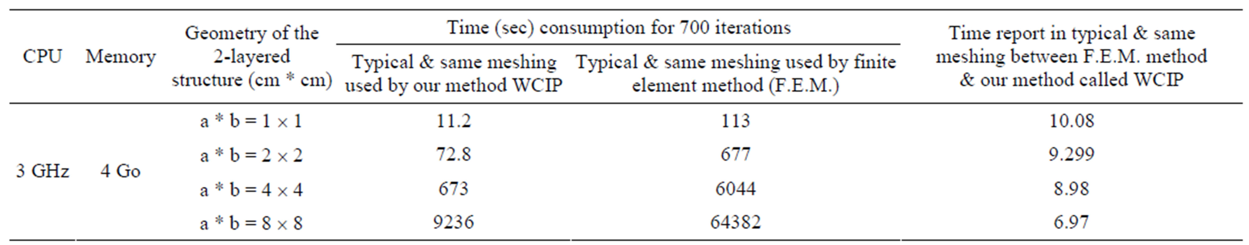
Table 1. Time report between typical meshing of different layers given in comparison between our so called method WCIP and Finite Element Method (F.E.M.) with a CPU 3 GHz and 4 Go of memory.
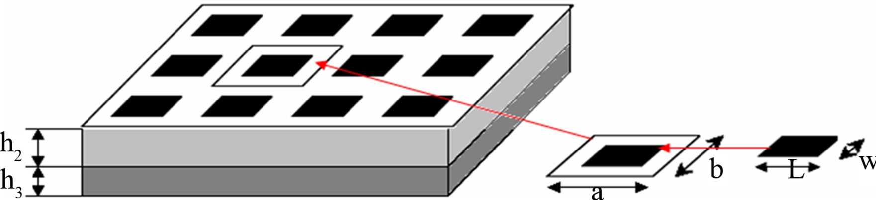
Figure 8. The grating of conducting plates in the particular case of rectangular plates.
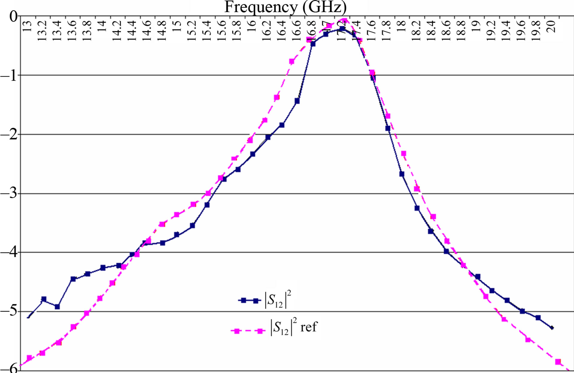
Figure 9. Variation of the transmission power versus frequency, a = b = 1 cm, w = 0.0625 cm, L = 0.6875 cm, h1 = h2 = 0.05 cm, εr1 = 2, εr2 = 1.

Figure 10. Variation of the reflected power versus frequency (GHz), a = b = 1.8 cm, w = 0.6 cm, L = 1.2 cm, h1 = h2 = 0.15 cm, εr1 = εr2 = 4.4.
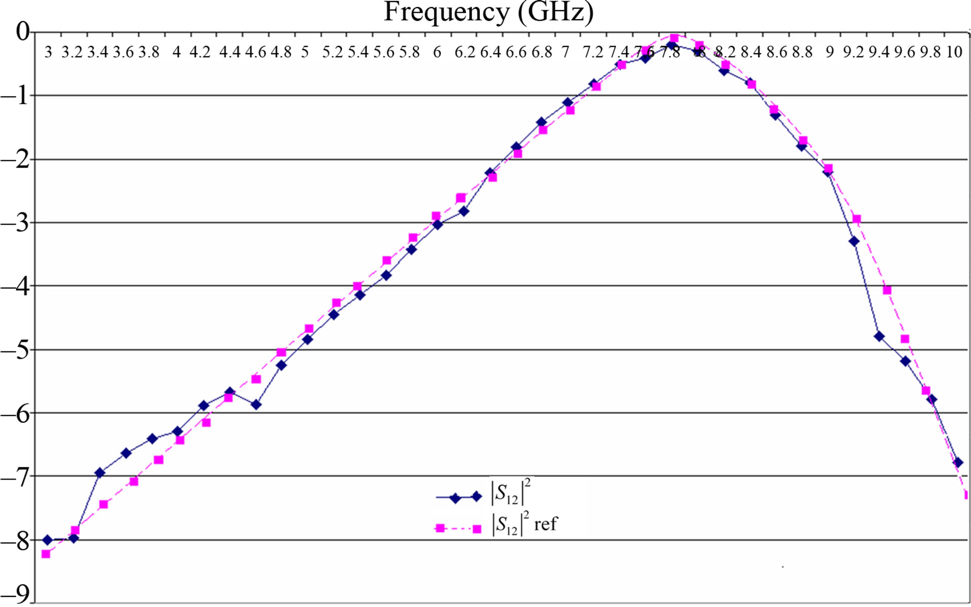
Figure 11. Variation of the transmission power versus frequency (GHz), a = b = 1.8 cm, w = 0.6 cm, L = 1.2 cm, h1 = h2 = 0.15 cm, εr1 = εr2 = 4.4.
We have presented in this application an approach to the full wave analysis of a double layered filter by our method called wave concept iterative process. The results show a good agreement between results given by our method and published data.
Other results of an oblique incidence are done and proved numerically and experimentally that the resonant frequencies are not so sensitive to both the angle of incidence and the incident polarization.
3.2. Application 2: Analysis of Novel Dual-Resonant and Dual-Polarized Frequency Selective Surface Using Eight-Legged
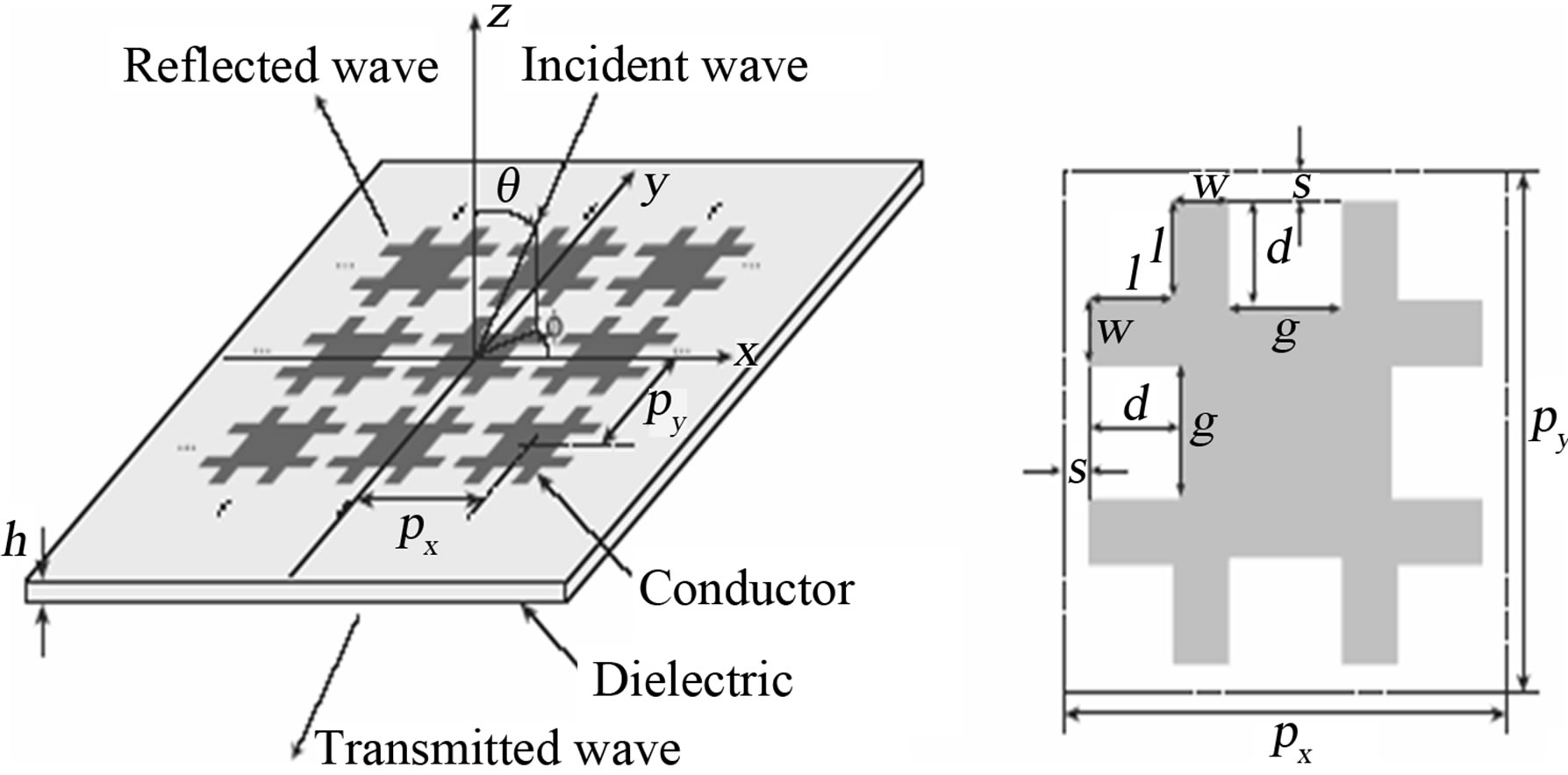
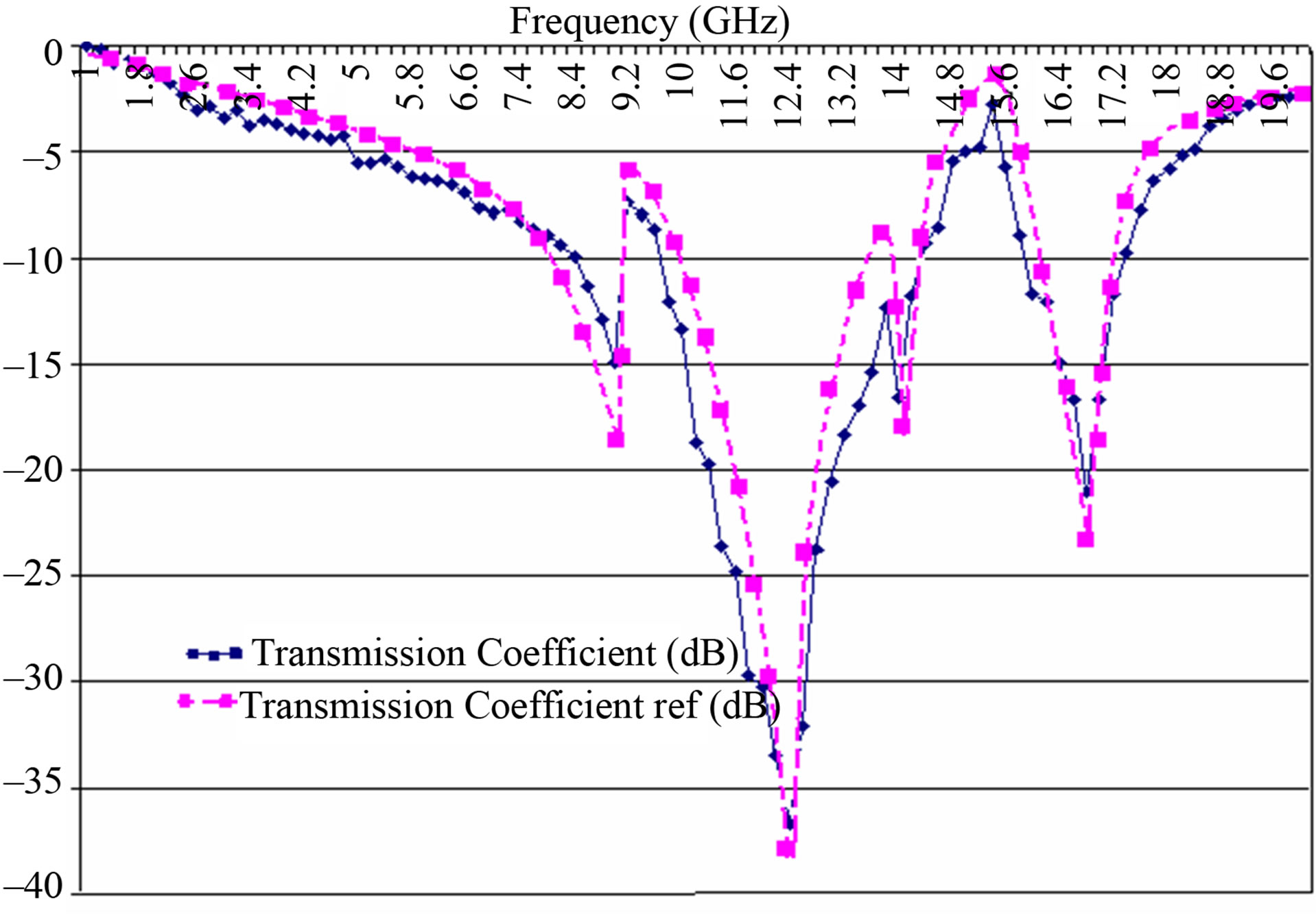
We propose, here, to analyze a new simple element that has two resonant frequencies for full reflection at dual band. The geometry is drastically simplified. The proposed patch element is called hereafter eight-legged element from the view point of the geometry. To prove the effecttiveness of the eight-legged element, the transmission responses at normal plane-wave incidence are evaluated for the proposed geometrical parameters. A grid of 128 by 128 pixels is used to define the interface with extreme fidelity to the geometric parameters. These results are obtained after 600 iterations. Also, the verification of the simulated results is performed by experiments [6]. This structure is described in Figures 12(a) and (b).
Figure 13 illustrates comparison of transmission response for the simulated results and experimental approach for FSS consisting of elements A and B shown in the inset, and the proposed eight-legged element in case of normal incidence.
Where Geometrical parameters: w = 1.38, l = 2.41, d = 2.41, g = 2.75, s = 0.34. Periodic spacing: px = py = 11.0 (unit: mm). Dielectric: εr = 4.3, h = 1.6 mm.
To prove the validity of our theory, the simulated results are performed for TE-wave oblique incidence. Here, TE waves stand for the electric field normal and parallel to the x-y plane. The periodic spacing of the FSSs shown in next figure is px = py = 11.0 mm. the geometric parameters are presented as follow: w = 1.38, l = 2.41, d = 2.41, g = 2.75, s = 0.34. Periodic spacing: px = py = 11.0 (unit: mm). Dielectric: εr = 4.3, h = 1.6 mm.
Figures 14(a) and (b) show the comparison of the transmission characteristics (θ = 20˚, φ = 0˚) & (θ = 35˚, φ = 0˚) between our approach and experimental results given by [6]. For the eight-legged element, the sharp dips appear at 9 and 14 GHz only for TE-wave oblique incidence. These singular resonances are caused by a characteristic current distribution [11,12], which significantly depends on the incident polarization.
As a result, we can assume that the transmission and reflection responses include the singular behaviors which are good agreements between the measured and the calculated results. It can be seen numerically and experimentally that the resonant frequencies are not so sensitive to both the angle of incidence and the incident polarization.
In addition, it is important to notice that consumption in memory and time of simulation results is limited in the sense that our method is a 2-D dimension.
3.3. Application 3: Analysis of Periodic Antenna Array with Double Face
The structure presented by Figure 15 is composed by a dielectric layer on which two identical forms are printed on each face. In fact, it is a multi-layer structure comprising two interfaces and three layers especially dielectric layer delimited by two layers of air with infinite thickness. The dielectric layer has a relative permittivity εr = 2.58 and a height d = 2.362 mm.
The structure is excited by a spectral incidental wave according to Y and with a normal angle of incidence on the surface (θ = φ = 0). A grid of 128 by 128 pixels is used to define the interface and the results are recorded after 800 iterations.
Results of simulation of reflexion and transmission coefficients of the multilayer antenna are compared with those obtained with method of moments [13].
 (a) (b)
Figure 12. FSS with eight-legged elements printed on a dielectric. (a) Two dimensional periodic structure; (b) Its unit cell.
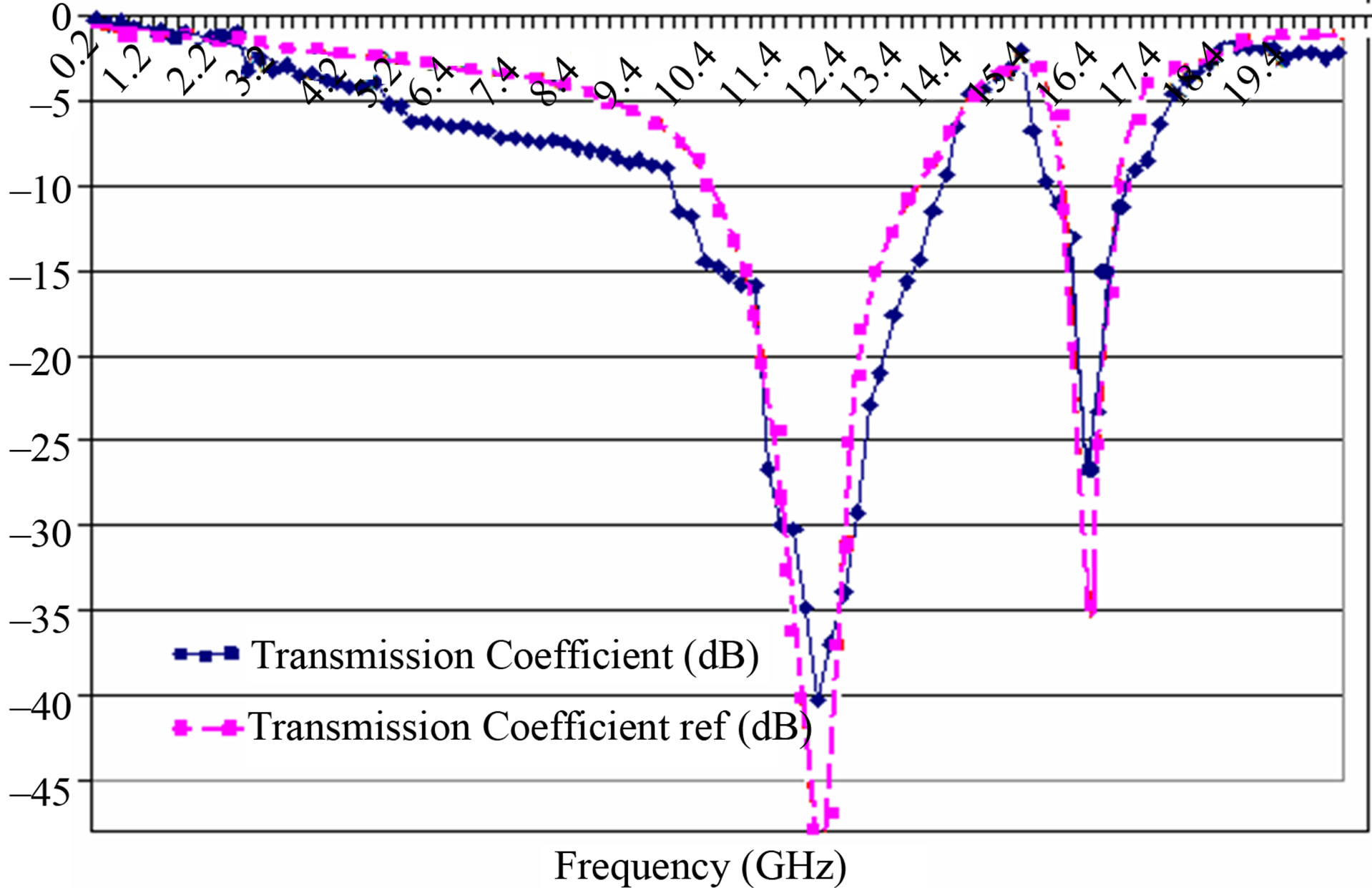
Figure 13. Comparison of transmission response for the simulated results and experimental approach for FSS consisting of elements A and B shown in the inset, and the proposed eight-legged element in case of normal incidence.
 (a)
(a)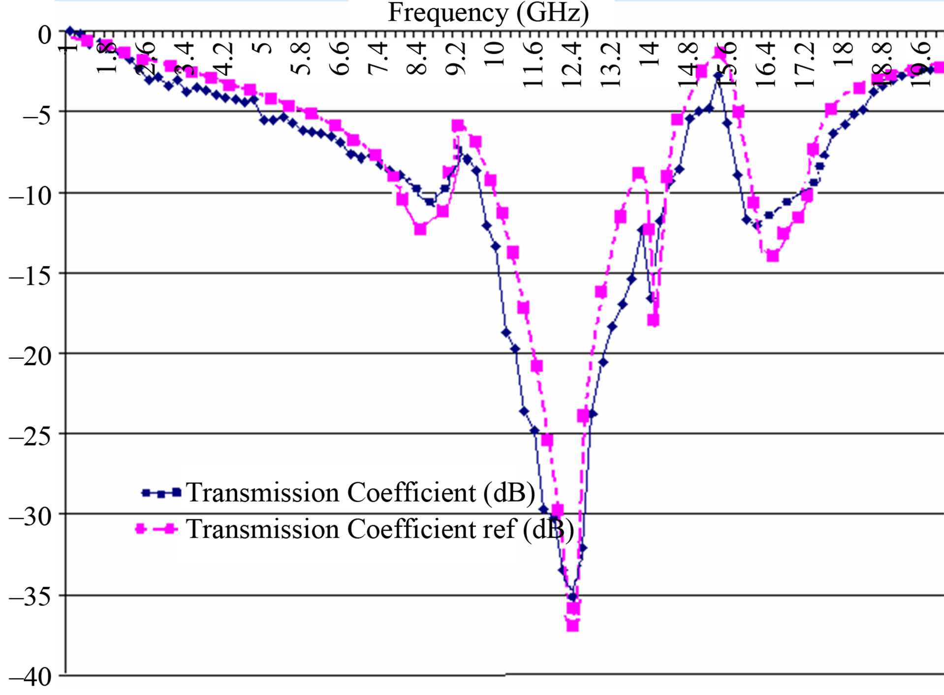 (b)
(b)
Figure 14. (a) Comparison of the frequency characteristics between the calculated and the measured results of the FSS with eight-legged element in TE-wave incidence at θ = 20˚; (b) Comparison of the frequency characteristics between the calculated and the measured results of the FSS with eight-legged element in TE-wave incidence at θ = 35˚.
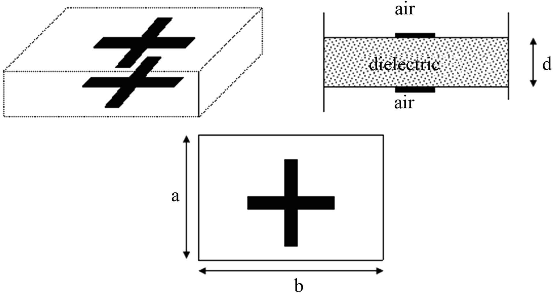
Figure 15. Periodic structure with double interface.
by the Figure 16, we have to note that there is an agreement in reflexion coefficient. In both cases, we observe a total band of reflexion around 15 GHz.
Other results of an oblique incidence are done and proved that singular resonances are caused by a characteristic
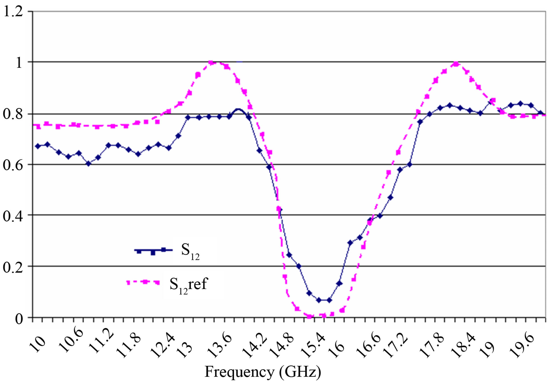
Figure 16. Comparison of transmission response for the simulated and experimental results versus frequency (GHz).
current distribution which significantly depends on the incident polarization. The transmission and reflection responses including the singular behaviors are in good agreements between the measured and the calculated results. It can be seen numerically and experimentally that the resonant frequencies are not so sensitive to both the angle of incidence and the incident polarization.
3.4. Application 4: Analysis of Frequency Selective Structure (FSS) Made of Perfectly Conducting Rectangular Patches Periodically Embedded in a Dielectric Slab
The structure presented by Figure 17 is frequency selective structure (FSS) made from perfectly conducting rectangular patches periodically embedded in a dielectric slab with a relative permittivity εr = 2. The computational unit cell is shown in Figure 17. We again consider both normal incidence and oblique incidence with, and for both cases the incident electric field is parallel to the longer side of the PEC patches. The results for the power reflection coefficient Pr for the normal and oblique incidence are shown in next figure, Figures 18 and 19, respectively.
The structure is excited by a spectral incidental wave according to Z and a normal angle of incidence on the surface (θ = φ = 0) then (θ = 30˚, φ = 0). A grid of 128 by 128 pixels is used to define the interface and the results are recorded after 800 iterations.
Results of simulation of the FSS are compared with those obtained by the Finite Element method [14]. They show a good agreement in Power reflexion coefficient in both cases, normal and oblique incidence in comparison with reference [14].
Both reference results are based on formulations in the frequency domain. For normal incidence, Figure 18, there is good agreement between the two methods as expected since there are no higher order modes present in
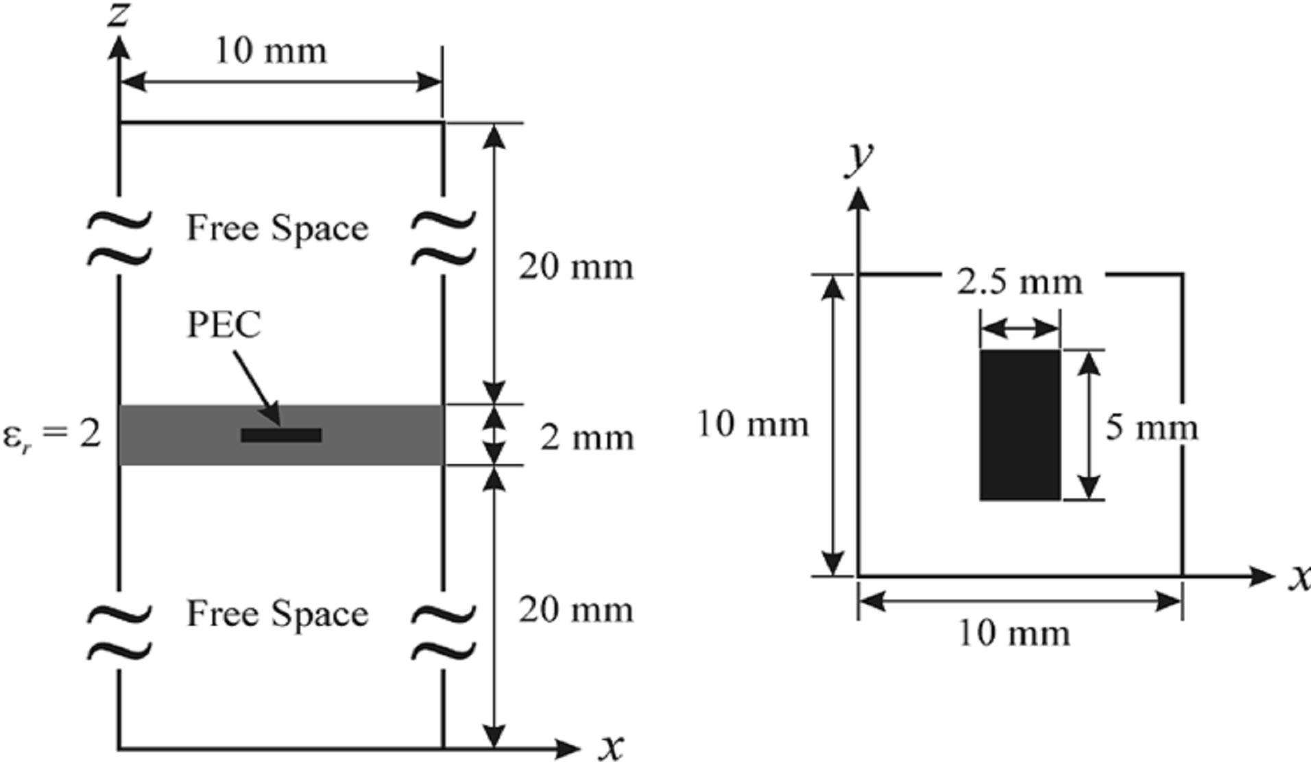
Figure 17. Description of the unit cell used for the PPMSWCIP computation of a FSS.
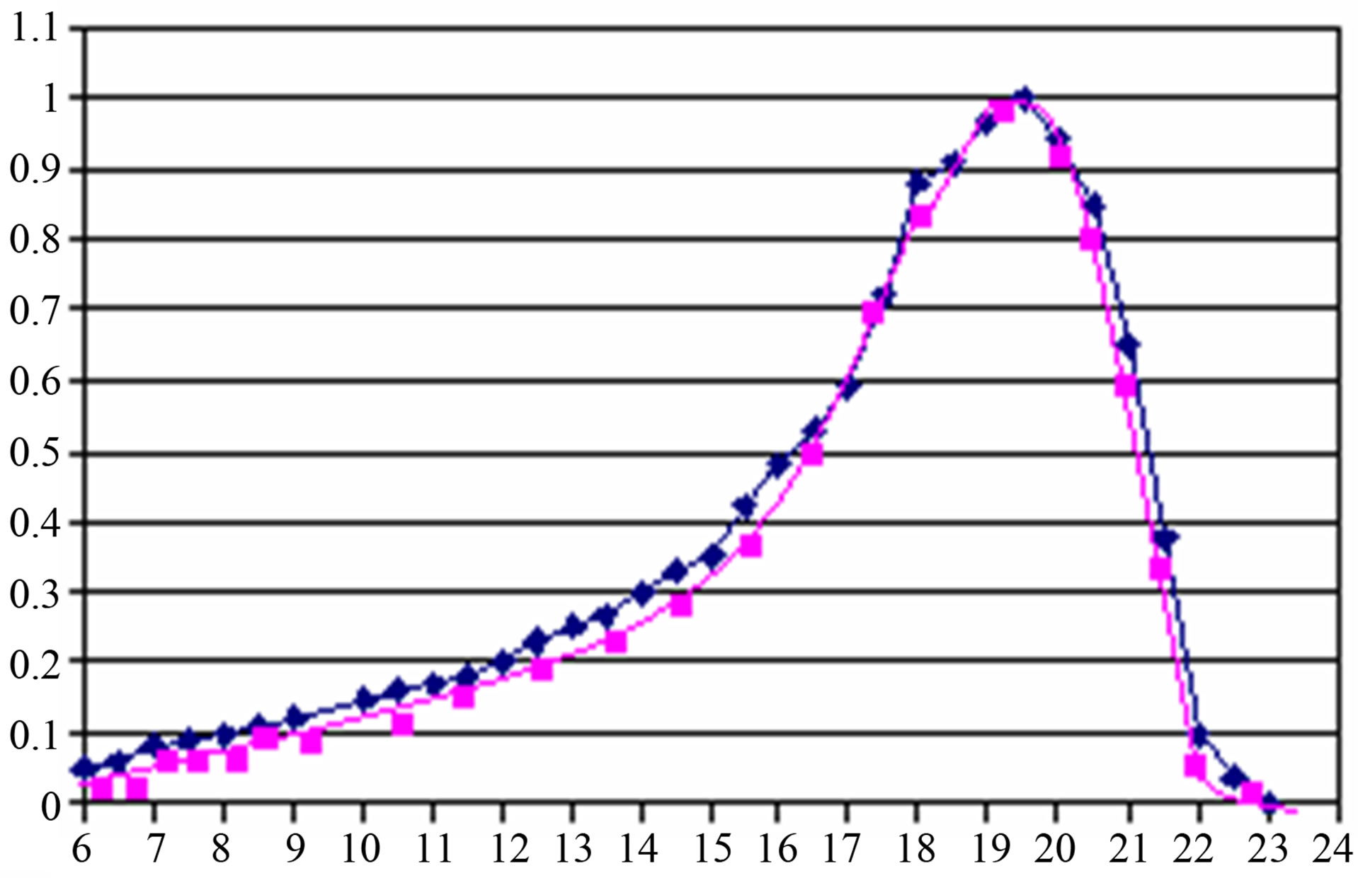
Figure 18. Power reflection coefficient as a function of frequency due to a plane wave incident on a FSS with a unit cell shown in Figure 17 in case of normal incidence with parallel electric field to the longest side of the PEC patches.
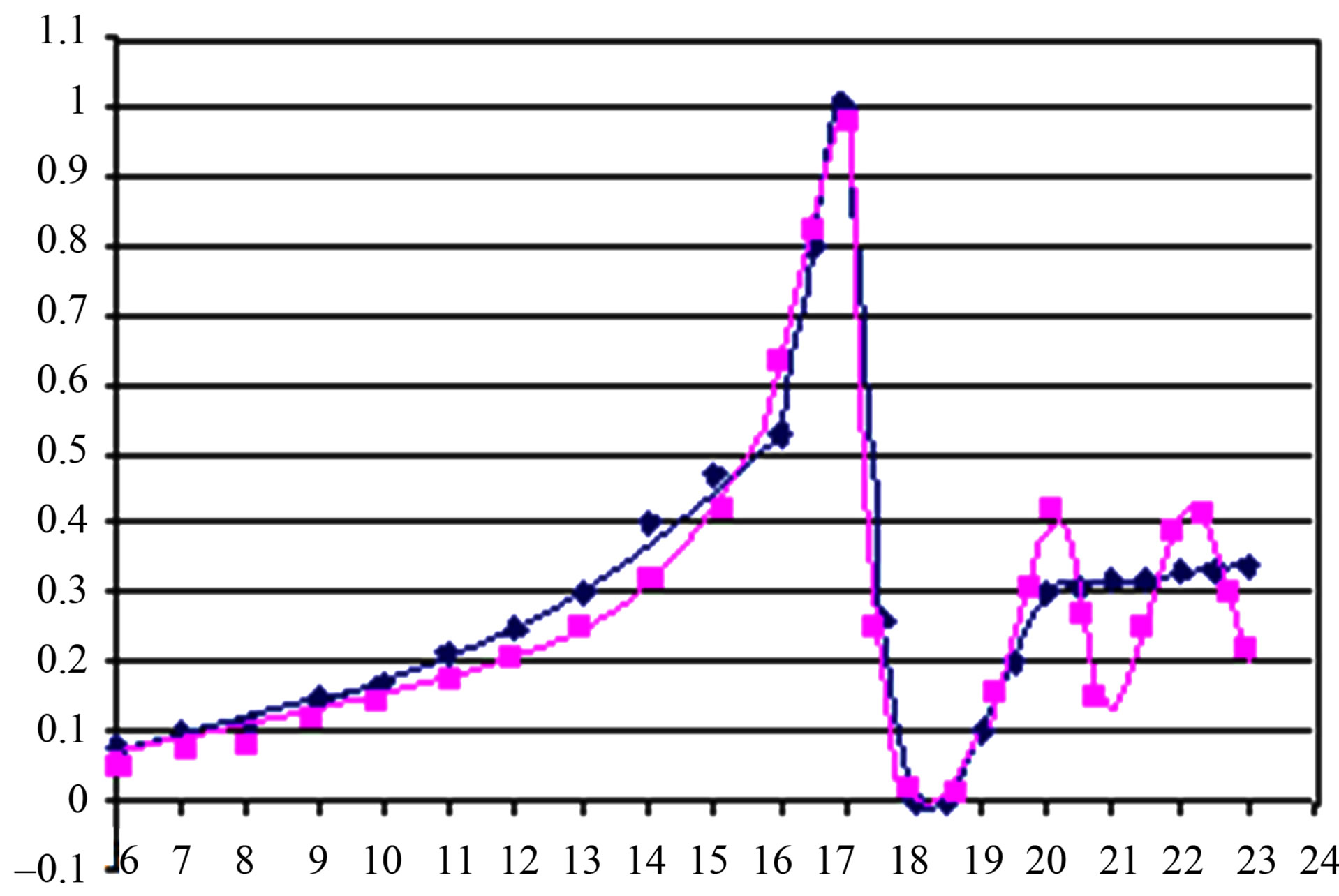
Figure 19. Power reflection coefficient as a function of frequency due to a plane wave incident on a FSS with a unit cell shown in Figure 17 in case of an oblique incidence θ = 30˚, φ = 0) with a parallel electric field to the longest side of the PEC patches.
the field solution for that frequency range concerning Finite Element Method (F.E.M.) and nonexistence of interpolations in our Wave concept Iterative Method. For oblique incidence, Figure 19, there is good agreement
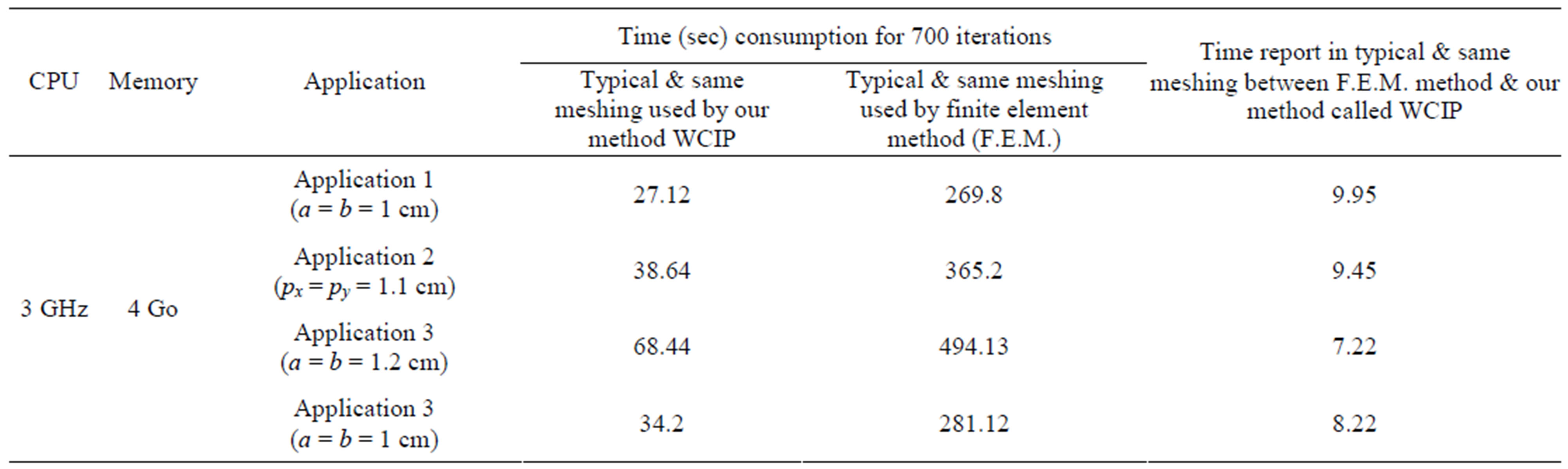
Table 2. Time report between typical meshing of different layers given in comparison between our so called method WCIP and Finite Element Method (F.E.M.) with a CPU 3 GHz and 4 Go of memory in case of each application.
between the two methods except for the frequencies above the cutoff frequency 20 GHz. The reason for the discrepancy is again attributed to the basis formulation of fem. method.
The main goal of the manuscript is the reduction of the computational effort required for the analysis of arbitrary microwave components. Therefore I have added a table that compares the performance of the proposed method vs F.E.M. method for all the applications reported in Paragraph 3. These results are proposed in Table 2. Those given results, and as expected, has became to prove the efficiency of our method and its capability to reduce the computational time and memory consumption in case of periodic planar multilayered structures analysis by Wave Concept Iterative Process method (WCIP).
4. Conclusions
The possibility of dynamically varying the number of layers in periodic planar multilayered structures and consequently the computation time 2D periodic structure in microstrip technology has been investigated numerically. In this sense, we have studied and described a series of periodic configurations involving periodic antenna and FSS arrays which produce well-defined absorption bands, with controllable absorption frequency. The critical frequency has been shown to be strongly influenced by the ratio period/plate-size, which therefore provides a good control parameter. Different geometric parameters have been shown to allow the control of the critical frequency.
A simple and efficient method for the analysis of the multilayer periodic patches was presented. Flexible selectivity was achieved when adopting periodic multilayer configuration of iterative method taking into account spectral approach in multilayer FSS and antenna study. By using simple relations, the multilayer problem was accounted for by the WCIP method in multilayered configuration without leading to a heavy computation time what is improved since it is greatly reduced compared with that of the conventional traditional methods. The choice of the number of pixels used to define the interface was based on achieving a compromise between the precision of the obtained results and the time consumption. But some approximation was necessary in modulation of geometric parameters by number of pixels in each interface. The resolution of this difficulty will be investigated in future work by micro and macro-pixels notion in division of each interface. Simulated results agree with measurements and literature. Moreover, the development of our method can be applied to a very important domain called quasi-optic in which active components (amplifier, diodes, transistors…) will be implemented. In this case, we can amplify energy and control frequency’s response of different structures by considering the tile approach of energy amplifier.
Other prospects are considered in study of quasi-optic structures in tray approach by iterative method which is now in development. Accordingly, many rectifications will be needed in different domain (spectral and spatial) and in different used equations.
REFERENCES
- B. Munk, “Frequency Selective Surfaces: Theory and Design,” Wiley, New York, 2000. doi:10.1002/0471723770
- T. K. Chang, R. J. Langley and E. A. Parker, “Frequency Selective Surfaces on Biased Ferrite Substrates,” Electronics Letters, Vol. 30, No. 15, 1994, pp. 1193-1194. doi:10.1049/el:19940823
- T. Ege, “Scattering by a Two Dimensional Periodic Array of Conducting Rings on a Chiral Slab,” IEEE Proceeding of Antennas and Propagation Society International Symposium, Vol. 3, 1996, pp. 1667-1670.
- A. L. P. S. Campos, M. A. B. De Melo and A. G. Assunção, “Scattering by FSS on Anisotropic Substrate for Te and Tm Excitation,” IEEE Transactions on Microwave Theory and Technology, Vol. Mtt-50, 2000, pp. 72-76. doi:10.1109/22.981249
- El A. Hajlaoui, H. Trabelsi, A. Gharsallah and H. Baudrand, “Analysis of Multilayer Substrates by Multilayer Contribution of Wave Concept Iterative Process (Mlc-Wcip),” Microwave and Optical Technology Letters, Vol. 49, No. 6, 2007, pp. 1439-1445. doi:10.1002/mop.22406
- M. Ohira, H. Deguchi, M. Tsuji and H. Shigesawa, “Novel Dual-Resonant and Dual-Polarized Frequency Selective Surface Using Eight-Legged Element and Its Experimental Verification,” IEICE Transactions on Electronics, Vol. e88-c, No. 12, 2005.
- El A. Hajlaoui, H. Trabelsi and H. Baudrand, “Analysis of Novel Dual-Polarized Frequency Selective Surface Using Periodic Contribution of Wave Concept Iterative Process: Ppms-Wcip),” 3rd International Conference Information and Communication Technologies: From Theory to Applications, ICTTA 2008, No. 7-11, 2008, pp. 1-6.
- H. Trabelsi, A. Gharsallah and H. Baudrand, “Efficient Analysis of via Hole Grounds by Using the Iterative Method,” Journal of Electromagnetic Waves and Application, Vol. 18, No. 2, 2004, pp. 265-277.
- M. Horno, “Calculation of Quasi-Static Characteristics of Microstrip on Anisotropic Substrate Using Mapping Method,” Microwave Symposium Digest, MTT-S International, Vol. 80, No. 1, 1980, pp. 450-452.
- A. L. P. S Campos, A. G. d’assunção and A. G. Neto, “Scattering Characteristics of FSS on Two Anisotropic Layers for Incident Co-Polarized Plane Waves,” Microwave and Optical Technology Letters, Vol. 33, No. 1, 2002, pp. 57-66. doi:10.1002/mop.10231
- M. Ohira, H. Deguchi, M. Tsuji and H. Shigesawa, “A Singular Characteristic of Single-Layer Frequency Selective Surface with the Element Optimized by Ga,” IEEE Topical Conference on Wireless Communication Technology, Honolulu, October 2003, No. S16p01.
- A. S. Barlevy and Y. Rahmat-Samii, “On The Electrical and Numerical Properties of High Q Resonances in Frequency Selective Surface,” In: J. A. Kong, Ed., Progress in Electromagnetics Research, EMW Publishing, Cambridge, 1999, pp. 1-27.
- C. H. Wan and J. A. Encinar, “Efficient Computation of Generalized Scattering Matrix for Analysing Multilayered Periodic Structures,” IEEE Transactions on Antenna and Propagation, Vol. 43, No. 4, 1995, pp. 1233-1242.
- L. E. R. Petersson and J.-M. Jin, “A Three-Dimensional Time-Domain Finite-Element Formulation for Periodic Structures,” IEEE Transactions on Antennas and Propagation, Vol. 54, No. 1, 2006, pp. 12-19. doi:10.1109/TAP.2005.861547