Journal of Electromagnetic Analysis and Applications
Vol.4 No.2(2012), Article ID:17671,8 pages DOI:10.4236/jemaa.2012.42010
A Survey on Recent Approaches in the Design of Band Notching UWB Antennas
![]()
1Department of Electronic Engineering, Islamic Azad University, Shahr-e-Qods Branch, Tehran, Iran; 2Department of Engineering, Islamic Azad University, Shahre Rey Branch, Tehran, Iran.
Email: mjahanbakht@yahoo.com, *aalotfi@ieee.org
Received November 30th, 2011; revised December 29th, 2011; accepted January 19th, 2012
Keywords: Ultra Wideband; Band Notching; Microstrip Antenna; Survey Paper
ABSTRACT
According to federal communication commission (FCC) rules, the 3.1 - 10.6 GHz band is allocated to the amateur ultra wideband (UWB) applications. On the other hand, the 5.15 - 5.825 GHz band is associated with the wireless LAN (WLAN) applications according to IEEE 802.11 and HIPERLAN/2 standards. Therefore, an unwanted intrusion will be expected between these two frequency requests. In This paper a comprehensive review will be done over a wide range of UWB microstrip antennas which all have the band notching property over the WLAN band to effectively avoid this interference. All the band notching techniques in the recent papers will be categorized in 4 distinct methods including the tuning stub, the shaped slot, the parasitic element, and the fractal geometry. A few typical papers will be introduced and evaluated in each category for declaration purposes. At last, a comparison will be done between these methods and the relative papers.
1. Introduction
Recently, ultra wideband technology has been used in a wide range of applications such as radars, telemetry, navigation, biomedical systems, mobile satellite communications, the direct broadcast system (DBS), global positioning systems (GPS), and remote sensing. The design of an appropriate antenna for these systems is one of the most important challenging tasks.
Studies for achievement of compact and broadband operations of microstrip antennas have increased and various designs have been proposed and implemented to enhance this effect. Many techniques like using a pair of notches at the lower corner of the patch [1], inserting a slot in the tapered radiating element [2], meandered ground plane [3], multi-folding techniques [4], stack shorted patch [5,6], using elliptical slot [7], and other techniques [8,9] have been reported to obtain wideband and small size of microstrip antennas.
These ultra wideband antennas are mainly designed to transmit and receive short electromagnetic energies. It is one of the main blocks in any UWB systems [10]. The frequency range of 3.1 - 10.6 GHz has assigned by FCC to the amateur applications to develop UWB systems [11]. This assignment motivated lots of designers to work and publish papers on this area [12,13]. In the other hand, the frequency range of 5.15 - 5.825 GHz is assigned to WLAN applications. As a matter of fact, amateur UWB systems might cause an interference with WLAN applications which ought to be considered as a serious factor in any UWB system design. Therefore the UWB antenna with a band-stop performance is needed to prevent this interference.
During the next sections, an article review and comparison will be done to evaluate different UWB antenna techniques and also to realize the methods which authors are used to notch any unwanted frequencies. It will be shown that, methods like using tuning stub, inserting shaped slot, using parasitic element, and implementing fractal geometry have been reported to reach this purpose.
2. Band Notching Techniques
2.1. Tuning Stub
In a work done by Abbosh [12], a complete design method for a compact uni-planar UWB antenna with sub-band rejection capability is presented. As can be seen in Figure 1, a tuning line resonator is incorporated in the coplanar waveguide feeder of the antenna to act as a band-stop filter, hence enabling the rejection of any undesired band within the pass band of the antenna.
Results of the simulation and measurement show that the designed antennas have a bandwidth from 3 GHz to more than 11 GHz. The results also reveal that the use of the resonator in the feeder of the antenna efficiently rejects any undesired sub-band such as 4.9 - 5.9 GHz.
Two samples of the proposed antenna were designed and manufactured. The designed antennas feature a compact size of 27 mm × 27 mm. Values of the design parameters for the antenna and the incorporated resonator were first calculated using the proposed design procedure in the paper and then optimized using the software Ansoft HFSSv10. These optimized dimensions are presented in Table 1.
As can be seen in Figure 1(a), the tuning stub is folded over the transmission line. Therefore the electromagnetic field will be coupled and the effective length of the stub would be slightly more than its actual size. This extra effective length has to be considered in the line calculation and needs some modifications. This makes the whole fabrication process moderate, compared to other band notching techniques.
Figure 1(c) shows variation of the VSWR with frequency for the developed antennas. The simulated and measured characteristics of the antenna without a resonator reveal UWB behavior with bandwidth from 3 GHz to more than 11 GHz assuming VSWR = 2 (or 10 dB return loss) as a reference. It is also clear from this figure that, for the antennas with a resonator, the undesired sub band was tuned out, whereas the wideband behavior of the antenna was maintained. The simulated and measured results are in good agreement.
The gain of the antennas with the resonator is about 2.2 dBi at the pass band, while it is less than −8 dBi at the rejected sub-band. But this structure suffers from a complicated structure besides the narrow cuts on the printed board which could make the fabrication process more risky.
2.2. Shaped Slot
In [13] two CPW-fed compact elliptical monopole UWB antennas are introduced with band rejection characteristic at the band used for wireless LAN applications. The antennas are fabricated on ultra thin (100 μm) liquid crystal polymer (LCP) and the band notch is caused by the presence of a resonating slot over the elliptical radiator.
The two investigated antennas have a U-shaped slot and a C-shaped slot respectively. From the presented return loss and VSWR measurements, the C-shaped slot causes a wider rejection band compared to the U-shaped slot that could be used for the design of UWB antennas with reconfigurable sub bands.
Both designs present almost identical radiation pattern
 (a)
(a) (b)
(b)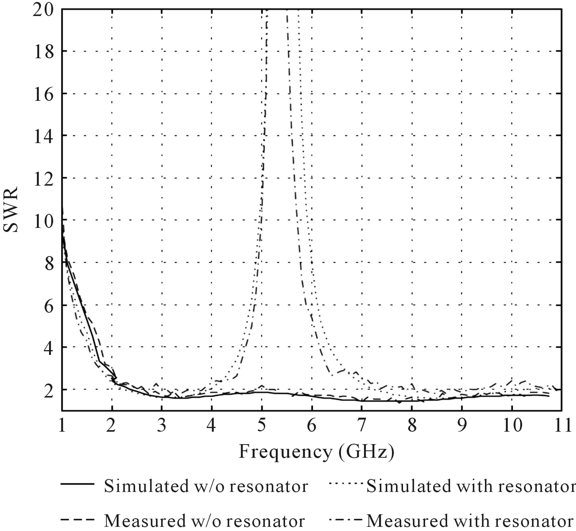 (c)
(c)
Figure 1. A typical λ/4 tuning stub as band notching resonator element. (a) Top view of the radiating patch; (b) A close look at the short circuited stub, and (c) Variation of the VSWR with frequency [12].

Table 1. Dimensions of the band notching tuning stub [12].
but as hinted out in the paper, the rejection band width is wide and the rejection frequency is far from the well known IEEE802.11a and HIPERLAN/2 frequencies.
In [14], two swallow-tailed ultra wideband planar monopole antennas that exhibit notch characteristics in the IEEE802.11a frequency band is introduced by inserting various slots into the antennas. The effects of the lengths of the slots on the notched frequency band are analyzed. The radiation patterns of the proposed antennas are also measured and the gains are shown to be flat, except in the notched frequency band. This antenna is actually a monopole structure in which the patch has been erected against the ground plane. This may cause some serious maintenance problems. Especially the narrow patch has to be hold by the central conductor of the coaxial cable.
An ultra wideband spiral slot microstrip antenna with variable frequency notching characteristic is presented in [15]. By inserting a variable length spiral cut within the radiating patch, different band stop frequencies are shown to be achievable.
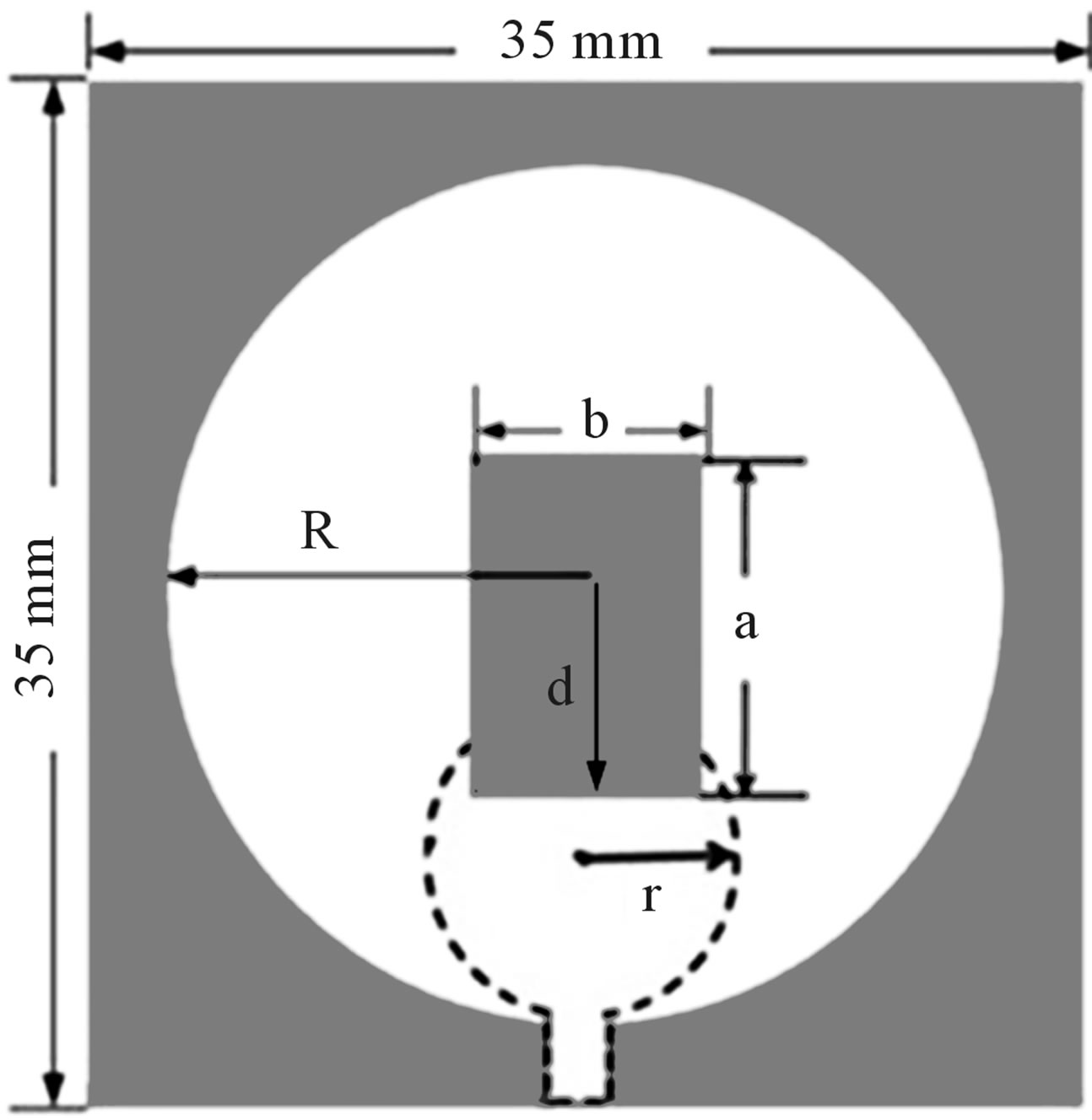
The designed antenna has the size of 35 × 35 mm2 which is at least 5.5% smaller in area compared to some of its counterparts. Figure 2 shows the configuration of the wideband antenna in [15] which consists of a circular patch with an etched spiral slot on the bottom view and also a circularly slotted ground plan with a printed rectangular patch on the top.
As can be seen, the spiral slot is printed over the circular termination of the feed line. The length and width of this spiral slot and other antenna dimensions are presented in Table 2. This antenna operates over the frequency range of 2.6 to 11 GHz and it rejects frequencies throughout the range of 5.2 to 5.9 GHz.
By creating a rectangular patch on the ground plan as a defected ground structure (DGS) an enhancement in bandwidth properties is achieved. This frequency bandwidth could easily be controlled by changing the shape and size of the rectangular DGS. The circular slot and rectangular DGS are both resonant structures and the combination of these two resonators widen the impedance bandwidth of the antenna.
After creating the rectangular DGS; by creating spiral slot on the circular patch, band notch characteristics will be achieved. This band notching spiral is sometimes hard to draw in simulating software and also in prototype PCB drawing tools. Therefore this band notching technique has a moderate fabricating difficulty, compared to the others.
The effect of the spiral cut on the VSWR has been investigated in Figure 2(c). As can be seen, the introduced spiral cut causes a frequency band rejection over any desired frequency range. Moreover the value of VSWR at the notch frequency is more than 4 that is reasonable for eliminating the WLAN interference.
 (a)
(a) (b)
(b) (c)
(c)
Figure 2. A typical spirally shaped slot to reject any unwanted frequency. (a) Top view of the radiating patch; (b) Bottom view of the feed line with an etched spiral slot, and (c) The effect of spiral slot on the VSWR characteristics [15].
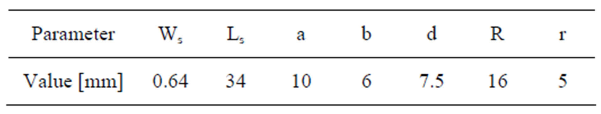
Table 2.Dimensions of the band notching shaped slot [15]
In [16] a novel band-notched microstrip slot antenna for UWB communication is presented. The antenna is comprised of elliptical stub that excite similarly shaped slot aperture. A H-shaped slot is filled in the elliptical stub. The proposed antenna is fabricated over RT/Duroid 6006 substrate to operate in UWB band (i.e., 3.1 - 10.6 GHz) and to reject the frequency band of 5.15 - 5.825 GHz.
The band notched characteristics of antenna is achieved by etching the H-shaped slot on the elliptical stub. Band notched characteristics can be controlled by proper adjusting of the H-shaped slot parameters.
The size of the antenna is 50 × 50 mm2 and the experimental results are in relatively good agreement with the analysis. Effects of varying the parameters of the Hshaped slot on the performance of the antenna have also been studied.
A new series of UWB antennas with unwanted frequency rejection specifications are proposed in [17]. In this reference an ultra wideband microstrip antenna with elliptical slot is introduces which could reject any desired frequency range by using an augmented crescent cut on the elliptically ended feed line. This rejection frequency is chosen to be 5.15 - 5.825 GHz.
The antenna parameters such as return loss, gain, and radiation pattern are calculated and the effect of dimensional variations on the antenna parameters has been studied. It has been shown that by changing some of these parameters, one may move or tighten the notching frequency bandwidth.
2.3. Parasitic Element
An ultra wideband antenna is proposed in [18] which entirely covers the frequency range of 3 - 12 GHz with an excessive band notching capability of frequencies in the range of 5.15 - 5.825 GHz which is assigned to WLAN applications.
It was claimed that the main idea of this paper could then be used beside most of the ultra wideband systems to avoid any unwanted intrusions to widely used wireless networks and communications. This band notching characteristic is achieved by using a crescent patch. The voltage standing wave ratio, radiation pattern, and effect of the crescent dimensions on the antenna parameters are studied.
The proposed antenna profile and schematic are presented in Figure 3. The microstrip feed line is used here to transmit electromagnetic wave to a polygonal termination line. Then, this wideband termination couples wave
 (a)
(a)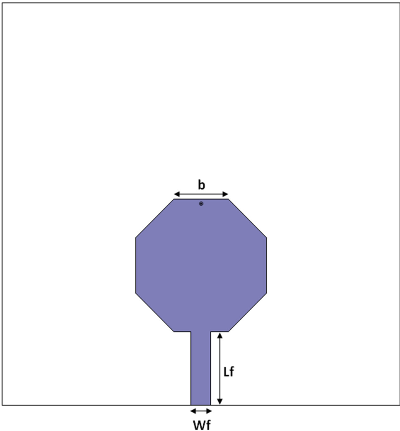 (b)
(b) (c)
(c)
Figure 3. A typical parasitic crescent to notch the UWB antenna. (a) Top view of the radiating patch and the parasitic patch; (b) Bottom view of the UWB hexagonal feed line, and (c) Measured and analyzed VSWR of the proposed antenna with and without the crescent patch [18].
to another polygonal radiating slot through the dielectric substrate. A series of typical dimensions of this paper are presented in Table 3. This antenna is quite easy to fabricate and to operate.
The intruded crescent patch acts mostly like an LC filter, resonating to reject any unwanted frequency bands. The length of this crescent patch affects the central rejection frequency and its width mainly specifies the rejection bandwidth.
The effect of the crescent patch is investigated in Figure 3(c). Without the crescent patch it is just an ultra wideband antenna which entirely covers 3 - 12 GHz and more. As can be seen, the parasitic crescent resonances in 5.5 GHz, absorbing the electromagnetic wave and obstructing any radiation.
In [19] a compact printed UWB antenna with bandnotched characteristic is presented. The antenna is designed to cover the FCC bandwidth for UWB applications (3.1 - 10.6 GHz) with band-notched at frequency band (5.15 - 5.825 GHz). The proposed antenna is fed by microstrip line, and it consists of square radiating patch on the top layer with a slotted-parasitic patch on the bottom layer of the antenna.
The parasitic patch acts as a notch filtering element to reject the desired frequency band. Moreover, the pulse distortions of different input pulses are investigated based on S21 parameters for two cases; face to face and side by side orientations. The major problem of this antenna is the return loss which sometimes increases to more than even 5 dB in the pass frequency bands.
In a work done by Fallahi et al. [20], a novel bandnotched elliptical slot antenna for UWB communication is proposed which is printed on a dielectric substrate of RT/Duroid 6006 with relative permittivity of 6.0, thickness of 1.27 mm, and fed by an elliptical open ended microstrip line connected to the 50 Ω main line. This antenna is designed to be used in frequency band of 3.1 - 10.6 GHz. Band notched characteristics of antenna to reject the frequency band of 5.15 - 5.825 GHz is realized by parasitic inverted-U strip attached to the elliptical slot plane. Effects of varying the parameters of parasitic inverted-U strip on performance of proposed antenna have been investigated. The antenna with optimal parameters obtained from parametric study is fabricated and measured.
2.4. Fractal Geometry
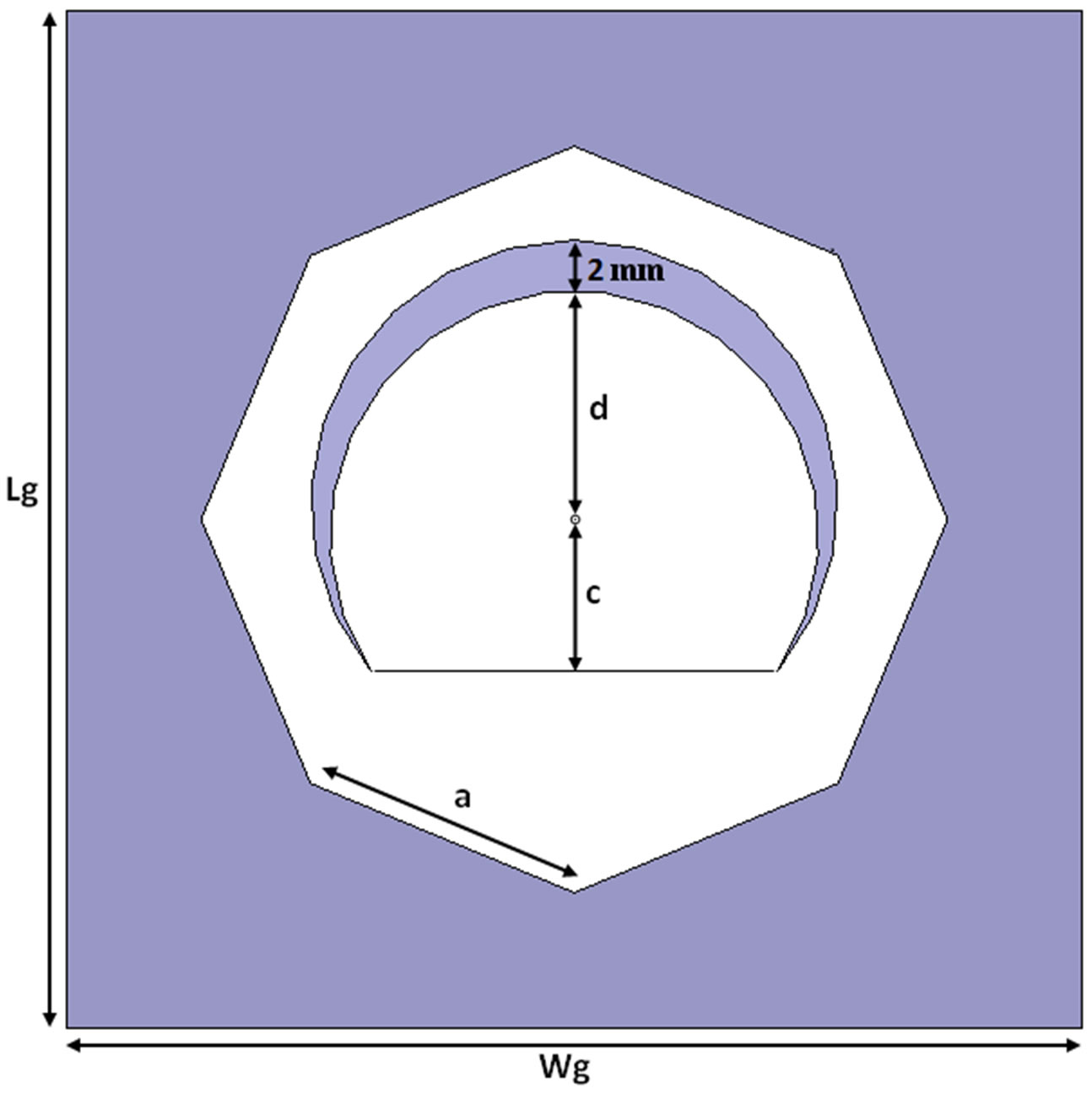
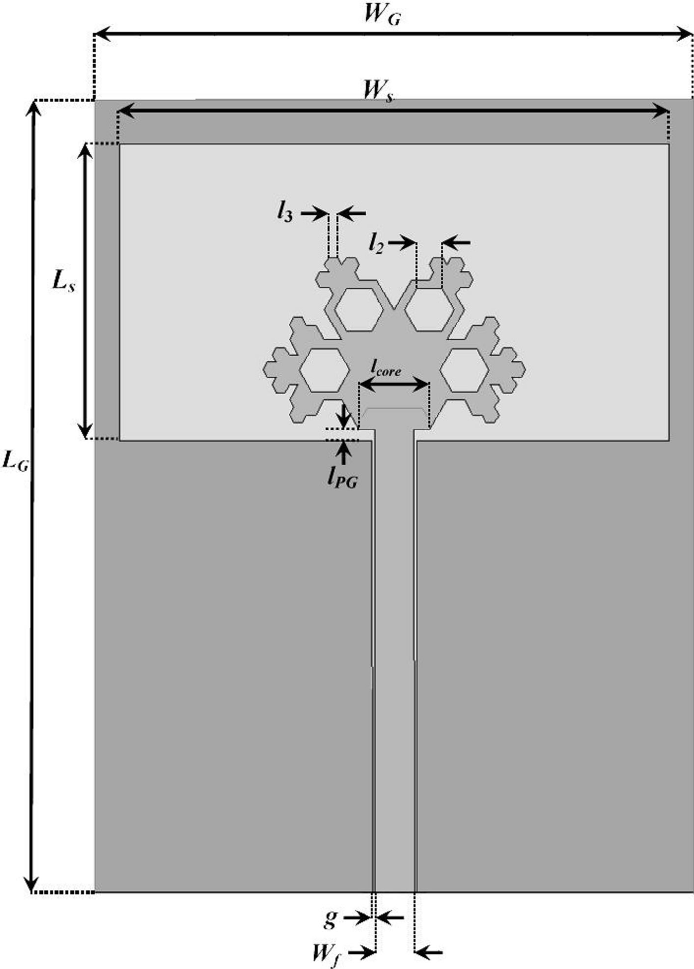
In [21] a band notched ultra wide band coplanar waveguide fed slot antenna is presented. A rectangular slot antenna is excited by a 50 Ω CPW line which is terminated to a fractal patch. The geometry of this band notched CPW-fed fractal antenna and its dimensions are depicted in Figure 4 and Table 4. This antenna has a simple structure with only one layer of dielectric substrate and metallization. These dimensions are obtained after performing an optimization.
The antenna was studied experimentally regarding impedance bandwidth and radiation patterns. For the proposed antenna, the −10 dB return loss bandwidth could reach 7.45 GHz (3.1 to 10.9 GHz) and a frequency notched band from 4.65 to 6.08 GHz was achieved.
The impedance band width for UWB design is about 111% with respect to the centre frequency of 7 GHz. Simulated and measured results on the return loss and the Eand H-plane radiation pattern of the proposed antenna are presented.
The effect of the central ring is investigated in Figure 4(c). With the change of the size of this ring and the arrow shaped stubs, it is easy to adjust the notch band width and center frequency.
3. Performance Comparison
In this section, a comprehensive comparison is done between different UWB antennas which all have the band notching behavior. In Table 5, the operating and rejection frequencies of the antennas are presented. In this
Table 3. Dimensions of the band notching parasitic element [18].
Table 4. Dimensions of the band notching fractal [18].

Table 5. Comparison of the operating frequency and band rejection technique between different UWB antennas.
 (a)
(a)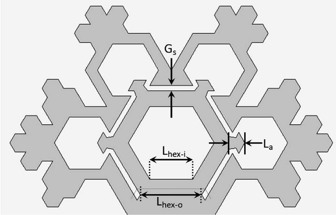 (b)
(b) (c)
(c)
Figure 4. A typical usage of the fractal geometry to reject unwanted frequencies. (a) CPW feed fractal antenna; (b) Close look at the fractal termination of the line, and (c) Return loss of the UWB antenna with and without the notching property [21].
table also the technique of each reference in creation of the notching behavior is named.
The size and the fabrication difficulties of each paper (including the used substrate name and its height and dielectric constant) has been presented in Tables 6 and 7.
The criteria to choose between easy and moderate fabrication difficulty is the smallest size (which is used in the antenna design) and also the curvature of the lines (such as circles and ellipses).
The average antenna gain in both pass band and rejection band (according to Table 5) are presented in Table 8. As a reason of the well known band notching property, the rejection gain is minus in dBi; compared to positive pass band gains.
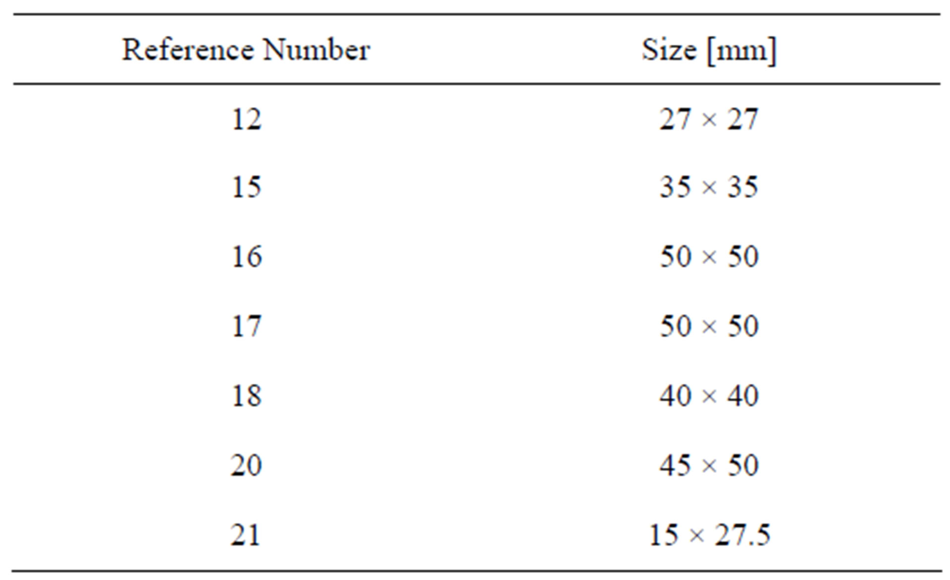
Table 6. Size comparison between different band notching UWB antennas.
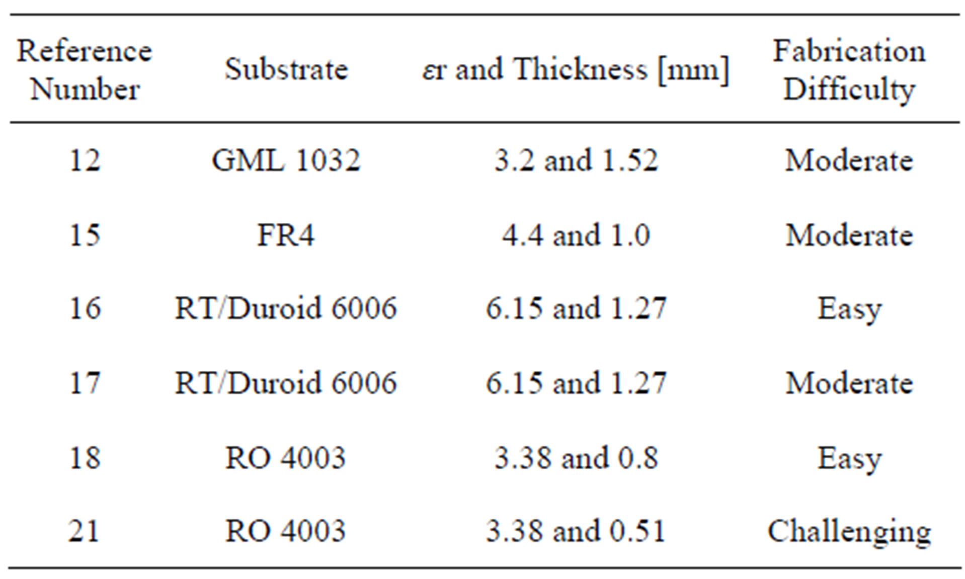
Table 7. Comparison of fabrication process between different band notching UWB antennas.

Table 8. Comparison of the gain between different band notching UWB antennas.
4. Conclusions
An extensive survey has been done over the recent UWB antennas with the band notching characteristics. All the methods; which were used by the authors, to notch the undesired frequencies are arranged in 4 separate categories including the tuning stub, the shaped slot, the parasitic element, and the fractal geometry. These categories were evaluated in different sections and relevant papers were introduced and studied in each section. Finally a comprehensive comparison has been done between the resources to compare their operating frequency, rejecting frequency, rejection technique used, size, fabrication process and difficulties, pass band gain, and rejection band gain.
Despite the fact that using fractal geometries makes the design and fabrication process more complicated, but it gives the designer a series of handful attributes. Fractals are generally non Euclidean geometries and they all have compact size, low profile, wide frequency bandwidth and conformal shape. The self similarity and space filling property makes them treat like an infinite length in a certainly finite area. By using these characteristics, smalller antennas can be designed in wider frequency bandwidths.
5. Acknowledgements
This work is published as a result of a research proposal named, “Design and Fabrication of an UWB Microstrip Antenna with Band Notching Property”. This proposal is approved and sponsored by Shahr-e-Qods Branch, Islamic Azad University and the authors want to acknowledge them.
REFERENCES
- J. Jung, W. Choi and J. Choi, “A Small Wideband Microstrip-Fed Monopole Antenna,” IEEE Microwave Wireless Component Letters, Vol. 15, No. 10, 2005, pp. 703-705. doi:10.1109/LMWC.2005.856834
- J. R. Verbiest and G. A. E. Vandenbosch, “A Novel Small-Size Printed Tapered Monopole Antenna for UWB WBAN,” IEEE Antenna Wireless Propagation Letters, Vol. 5, No. 1, 2006, pp. 377-379. doi:10.1109/LAWP.2006.881920
- J. S. Kuo and K. L. W. Ong, “A Compact Microstrip Antenna with Meandering Slots in the Ground Plane,” Microwave and Optical Technology Letters, Vol. 29, No. 2, 2001, pp. 95-97. doi:10.1002/mop.1095
- G.-M. Zhang, J. S. Hong, B.-Z. Wang, Q. Y. Qin, J. B. Mo and D.-M. Wan, “A Novel Multi-Folded UWB Antenna Fed by CPW,” Journal of Electromagnetic Waves and Applications, Vol. 21, No. 14, 2007, pp. 2109-2119. doi:10.1163/156939307783152911
- J. Ollikainen, M. Fischer and P. Vainikainen, “Thin Dual Resonant Stacked Shorted Patch Antenna for Mobile Communications,” Electronic Letters, Vol. 35, No. 6, 1999, pp. 437-438. doi:10.1049/el:19990324
- R. Brian, “Broadband Stacked Shorted Patch,” Electronic Letters, Artech House, Vol. 35, 1999, pp. 98-100.
- S. Angelopoulos, A. Z. Anastopoulos, D. I. Kaklamani, A. A. Alexandridis, F. Lazarakis and K. Dangakis, “Circular and Elliptical CPW-Fed Slot and Microstrip-Fed Antennas for Ultra Wideband Applications,” IEEE Antennas and Wireless Propagation Letters, Vol. 5, No. 1, 2006, pp. 294-297. doi:10.1109/LAWP.2006.878882
- K. P. Ray and Y. Rang, “Ultra Wideband Printed Elliptical Monopole Antennas,” IEEE Transactions on Antennas and Propagation, Vol. 55, No. 4, 2007, pp. 1189- 1192. doi:10.1109/TAP.2007.893408
- T. Yang and W. A. Davis, “Planar Half-Disk Antenna Structures for Ultra Wideband Communications,” IEEE Antennas and Propagation Society International Symposium, Vol. 3, 2004, pp. 2508-2511.
- K. Y. Yazdandoost and R. Kohno, “Ultra Wideband Antenna,” IEEE Communications Magazine, Vol. 42, No. 6, 2004, pp. S29-S32. doi:10.1109/MCOM.2004.1304230
- K. N. Modha, B. Hayes-Gill and I. Harrison, “A Compact, Low Loss Ice Cream Cone Ultra Wideband Antenna,” Seminar on Ultra Wideband Systems, Technologies, and Applications, London, 20 April 2006, pp. 165-168. doi:10.1049/ic:20060502
- A. M. Abbosh, “Design of a CPW-Fed Band-Notched UWB Antenna Using a Feeder-Embedded Slot Line Resonator,” International Journal of Antennas and Propagation, Vol. 2008, 2008, Article ID: 564317. doi:10.1155/2008/564317
- S. Nikolaou, B. Kim, Y.-S. Kim, J. Papapolymerou and M. M. Tentzeris, “CPW-Fed Ultra Wideband (UWB) Monopoles with Band Rejection Characteristic on Ultra Thin Organic Substrate,” Proceedings of Asia-Pacific Microwave Conference, Yokohama, 12-15 December 2006. doi:10.1109/APMC.2006.4429804
- H. J. Zhou, Q. Z. Liu, Y. Z. Yin and W. B. Wei, “Study of the Band-Notch Function for Swallow-Tailed Planar Monopole Antennas,” Progress in Electromagnetic Research, PIER 77, 2007, pp. 55-65. doi:10.2528/PIER07072506
- N. Bayatmaku, M. Naser-Moghadasi M. Jahanbakht and B. S. Virdee, “A Compact Ultra Wideband Printed Spiral Slot Antenna with Band Notched Characteristics,” Journal of Telecommunications, Vol. 3, No. 2, 2010, pp. 29- 31.
- A. A. Lotfi Neyestanak and A. A. Kalteh, “Band Notched Elliptical Slot UWB Microstrip Antenna with Elliptical Stub Filled by the H-Shaped Slot,” Journal of Electromagnetic Waves and Applications, Vol. 22, No. 14-15, 2008, pp. 1993-2002. doi:10.1163/156939308787537973
- M. Jahanbakht, A. A. Lotfi Neyestanak, and I. Vakili, “Band Notching Ultra Wideband Microstrip Antenna with an Augmented Crescent Cut,” 3rd European Conference on Antennas and Propagation, Berlin, 23-27 March 2009, pp. 3352-3355.
- M. Jahanbakht, A. A. Lotfi Neyestanak, E. Vakili, M. N. Moghaddasi and R. A. Sadeghzadeh, “Augmented Crescent as a Band Notching Patch to an Ultra Wideband Microstrip Antenna,” Journal of Electromagnetic Waves and Applications, Vol. 23, No. 11-12, 2009, pp. 1545-1554. doi:10.1163/156939309789476293
- N. H. M. Sobli and H. E. Abd-El-Raouf, “Design of a Compact Printed Band-Notched Antenna for Ultra Wideband Communications,” Progress in Electromagnetic Research M, Vol. 3, 2008, pp. 57-78. doi:10.2528/PIERM08051203
- R. Fallahi, A.-A. Kalteh and M. G. Roozbahani, “A Novel UWB Elliptical Slot Antenna with Band-Notched Characteristics,” Progress in Electromagnetic Research, PIER 82, 2008, pp. 127-136. doi:10.2528/PIER08022603
- A. A. Lotfi Neyestanak, M. R. Azadi Naeini, M. NaserMoghadasi and Gh. Dadashzadeh, “Band Notched CPW Fed Hexagonal Fractal Antenna,” Journal of Electromagnetic Waves and Applications, Vol. 23, No. 17, 2009, pp. 2461- 2470.
NOTES
*Corresponding author.