Natural Science
Vol.6 No.11(2014), Article
ID:47902,7
pages
DOI:10.4236/ns.2014.611082
The Chemical State of a Silver-Copper Complex Image Formed during the Electroless Copper Deposition
Yiheng Zhang*, Xingjian Li, Zijiang Yang
College of Chemistry and Molecular Engineering, Qingdao University of Science & Technology, Qingdao, China
Email: *yhzqust@163.com, lixingjian1314@163.com, yangzijiang09@yahoo.de
Copyright © 2014 by authors and Scientific Research Publishing Inc.
This work is licensed under the Creative Commons Attribution International License (CC BY).
http://creativecommons.org/licenses/by/4.0/


Received 20 May 2014; revised 22 June 2014; accepted 30 June 2014
ABSTRACT
By means of electroless copper deposition method a complex image has been fabricated in a mixture of cupric sulphate and formaldehyde, the surface and subsurface properties of which has been studied in detail by X-ray photoelectron spectroscopy (XPS) combined with sputter depth profiling technique analyzing distribution and chemical state of copper and silver. Depth profiling by XPS in conjunction with Ar+ sputtering shows that the catalytic activity of silver persists, catalyzing reduction of copper. The integral areas of spectra Ag3d after electroless copper deposition for 5 min at different sputtering times demonstrate that the amount of silver at the surface is greater than that in the interior. And then, the quite likely reasonable explanations are provided for the result. Additionally, the chemical shift of Ag3d XPS and deconvolution of Ag3d XPS spectrum have been also analyzed respectively at length.
Keywords:Electrochemistry, Electroless Copper Deposition, Imaging Agents

1. Introduction
The development of the technology of ultrafine printed wires is closely related to the design and the production of sophisticate electronic devices [1] -[3] . In comparison with those methods, such as plasma vapor deposition, chemical vapor deposition and electroplating technology, electroless plating not only is a simple and convenient method particularly with respect to its cost performance and very simple equipment, but also has the following superiorities: 1) a layer of conductive material can be deposited directly onto the dielectric substrate without an electric source; 2) any surface including 3-D and internal structures with complicated shape can be uniformly metallized by electroless deposition [4] -[6] . Therefore, electroless metal deposition has played an important role in the fabrication of very large-scale integrated circuits and ultra large scale integrated circuits [7] . The flowchart of integrated circuits fabricated by electroless deposition method is showed in Scheme 1. Moreover, electroless copper deposition has become an important research field and been widely applied because of low bulk electrical resistivity (1.67 mWcm) and the high resistance to electromigration of copper [8] [9] .
A silver image obtained when a silver halide photographic material is exposed and processed can be used under certain conditions to catalyze a redox reaction depositing another metal, for example, copper onto the silver image. The process not only is equivalent to the widely used electroless metal deposition method, but also has a close relation with the photographic process. In a modern photographic process, coordination compounds are doped in silver halide microcrystals to produce shallow electron trap centers in order to greatly improve the sensitivity of the photographic emulsion [10] [11] . Shallow electron trap centers are believed to play an important role in the formation of the latent image in the silver halides grains when they are exposed. In general, shallow electron trap centers in silver halides can act as a temporary storage for a portion of photogenerated electrons in the interior of the microcrystals, resulting in reducing the recombination of electrons with holes. Thereby those shallow centers trapped electrons may migrate to the latent image centers at an opportune moment and increase the formation efficiency of the latent image in the photographic process.
The image silver formed by conventional development has no catalytic activity on electroless copper deposition because of the actions of Na3S2O3 in fix solution. It must be activated by rehalogenating the image silver to silver bromide. The silver bromide in turn is reduced to silver during the electroless copper deposition. The newly formed silver is catalytic and can act as the active center to catalyze electroless copper deposition. Copper deposits in the pattern of the original silver image. In comparison with other deposition methods, this new technique has matchless superiority in clarity, contrast and resolution of the image system.
The activation reaction is:

The reactions of electroless copper deposition are:


X-ray photoelectron spectroscopy (XPS) has been used extensively over the past ten years in many areas of surface and materials. One of the major advantages of XPS is its ability to provide consistent chemical information. XPS combination with sputter depth profiling technique also provides a detailed knowledge of the spatial distribution of specific elements and the changes of the chemical information in both the surface and the subsurface. In this study, the distribution and chemical state of copper and silver within the final image are studied by alternative Ar+ sputtering and electron spectroscopy for chemical analysis (ESCA).
2. Experimental and Methods
The tabular grain silver halide emulsions, prepared by means of equilibrium double-jet methods, are used as the light-sensitive material to be coated onto a substrate. The samples are divided into two groups. One group (Sample A) is without shallow electron trap dopants, and another one (Sample B) is doped with shallow electron trap dopants (K3Fe(CN)6) during the manufacture of emulsions. After uniform exposure (daylight, 0.05 sec), both groups of samples are developed in D-19 (20˚C, 5 min) and fixed in F-6 (20˚C, 10 min). After fixation the samples were washed thoroughly in running water to ensure that there was no residual Na2S2O3 and hence no S in the emulsion layers. Followed activation the samples are developed in an electroless copper deposition solution, which contains mainly cupric sulphate and formaldehyde (pH = 13.0). The formulas of activating solution and electroless copper deposition solution are shown in Table1
To obtain information on depth distribution of copper and silver, the Ar+ sputtering and ESCA analysis are performed alternately at the same position in the image area by an XPS, Perkin-Elmer Model PHI-550 (Norwalk, CT). The pressure in the ultrahigh vacuum chamber of the spectrometer is 666.6610−10 Pa. The Mg Ka with photon energy hn = 1253.6 eV is used as a radiation source. All binding energies are referenced to a C1s neutral carbon peak at 284.6 eV. The characteristic peaks of Ag3d3/2 (367.9 eV) and Cu2p3/2 (932.4 eV) are used in
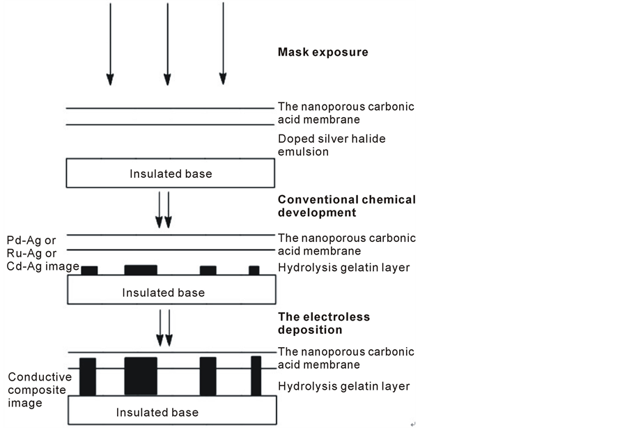
Scheme 1. The fabrication of integrated circuits via electroless copper deposition.

Table 1. Experimental formula.
silver and copper analysis respectively.
3. Results and Discussion
3.1. Depth Profiling by XPS Combined with Ar+ Sputtering
Sputter depth-profiling technique (such as Ar+ etching in situ) in combination with X-ray photoelectron spectroscopy will be used to understand the surface and the subsurface properties of a complex image formed during electroless copper deposition. The depth profiles for the sample A and B treated with activating solution for 10 min, followed by electroless copper deposition for 5 min, respectively are shown in Figure 1(A) and Figure 1(B). Figure 1 indicates that silver initially formed is not completely covered by copper formed by the catalysis of newly formed silver and copper. The catalytic activity of silver persists, catalyzing further reduction of copper. The integral areas of spectra Ag3d at different sputtering times indicate that the amount of silver at the surface is greater than that in the interior. Maybe this can be explained as following: 1) The sizes of the silver atom and the copper atom are not matched, and the stress in the crystal lattice caused by the deposit of copper forces silver atoms to diffuse to the image surface. 2) The specific surface free energy of silver (ΓAg = 1.53 × 10⁻⁴ J∙cm−2) is less than that of copper (ΓCu = 1.67 × 10⁻⁴ J∙cm−2), and when the two metals coexist, the metal having
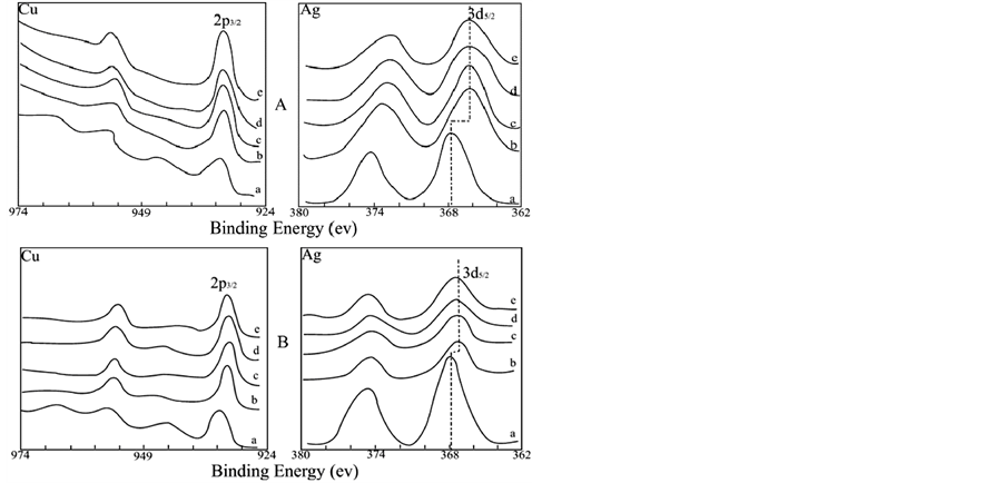
Figure 1. Cu2p and Ag3d XPS with Ar+ sputtering. Panel A: sample A; Panel B: sample B. Ar+ sputtering time: a. 0 (surface); b. 5 min; c. 15 min; d. 25 min; e. 35 min.
the lower specific surface energy is concentrated at the surface more readily. 3) Perhaps the Ag+ is complexed by EDTA and is then deposited by reduction.
Copper at the surface may be oxidized to a certain degree. With increase of the time of electroless copper deposition the amount of copper deposited at the surface increases, and more copper is oxidized. Curve a, the XPS spectra at the surface, in Figure 1(A) and Figure 1(B), respectively show a typical CuO 2p XPS spectrum (the binding energy of CuO is 933.6 eV) [12] .
If electroless copper deposition continues long enough, a bright and electrically conductive copper film can be formed. XPS investigation of the sample shows that there is no silver at the bright surface, but after 60 min Ar+ sputtering, both silver and copper are found, as shown in Figure 2, indicating that although silver atoms tend to diffuse to the image surface, they are eventually covered by closely packed copper atoms. The continuation of electroless copper deposition after complete covering means that from then on the deposition is an autocatalytic one [13] [14] . The longer the deposition goes, the thicker the pure copper layer becomes.
3.2. Chemical Shift
Figure 1(A), Figure 1(B) and Figure 2 show that all XPS spectra in the image exhibit a significant chemical shift to lower value for Ag3d, whereas no such shift is found for Cu2p, because the surface XPS data show the information of CuO instead of Cu. The data are listed in Table2 As the atomic combination state and the chemical circumstances around the atoms are changed, the accurate value of binding energy for the internal energy level may vary. The chemical shift of silver obtained from electroless copper deposition indicates that electron clouds of 5s orbital of the outmost shell of the silver atoms partly overlap with each other, forming metal bonds, and hence silver clusters Agn, with a number of silver atoms are formed. However, the position of Agn peak may vary because at different positions and depths the number of silver in the cluster may different. In the silver cluster the partly overlapped 5s electron clouds are shared by all silver atoms, decreasing the shield effect for the electrons at the internal shells (3d) and causing the shift of the binding energy of 3d orbital to a lower value. The data listed in Table 2 state that under the same conditions (for example, at the same sputtering depth), the Ag3d chemical shift of the sample A (without shallow electron trap dopants) is more than the one of the sample B (doped with shallow electron trap dopants). These results also indicate that the rate of copper deposition for sample B is faster than for sample A under the same conditions of electroless deposition. Because with increase of the amount of copper deposition the relative amount of silver decreases, and at the same time the diffusion of silver atoms to the surface forced by crystal lattice stress, decreases the number of silver atoms in the silver cluster. Therefore the number of atoms whose 5s orbital electron clouds are partly overlapped
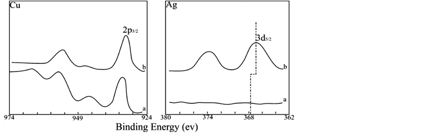
Figure 2. Cu2p and Ag3d XPS for sample with bright copper. Curve a. surface; Curve b. 60 min Ar+ sputtering.
Table 2. The chemical shift of Ag3d XPS.
decreases, as does the shield effect for the internal electrons, so that the chemical shift becomes less.
3.3. Deconvolution of Ag3d XPS Spectrum
With the aid of a computer the experimental XPS spectrum of Ag3d (sample A after 5 min sputtering) is deconvoluted [15] . The results shown in Figure 3, where the solid curve represents the experimental XPS spectrum and the dotted curves represent the spectra after the computer deconvolution, indicate that the experimental XPS spectrum consists of two spectra, one for Ag and the other for Agn. The result predicts that there must be two chemical states of silver in the image: monoatomic silver and polyatomic silver, as summarized in Table3 The integral areas shown in Table 3 are the areas under the spectral curves of monoatomic silver and polyatomic silver respectively. The ratio of the two areas is equal to the mol ratio of atoms existing in two different chemical states, Ag/Agn = 0.55. Because of the existence of monoatomic silver the crystal lattice stress owing to the deposition of copper can easily force silver atoms to diffuse from the interior to the surface. The data listed in Table 2 indicate that there is no chemical shift of Ag3d at surface, proving that silver at the image surface is in only a monoatomic state.
4. Conclusions
In summary, by analyzing the surface and the subsurface properties of a complex image formed during the electroless copper deposition by means of X-ray photoelectron spectroscopy combined with sputter depth profiling technique can draw the following conclusions:
1) Silver initially formed is not completely covered by copper formed by the catalysis of newly formed silver and copper by electroless copper deposition, which is an autocatalytic one after copper atoms completely covering silver atoms, subsequently shaping the increasingly thick copper layer until depletion of any active constituents in the plating baths.
2) The typical CuO2p XPS spectrums demonstrating copper at the surface may be oxidized to a certain degree. With increase of the time of electroless copper deposition the amount of copper deposited at the surface increases, and more copper is oxidized.
3) The chemical shift of Ag3d XPS proves electron clouds of 5s orbital of the outmost shell of the silver atoms partly overlaps with each other, forming metal bonds, and hence silver clusters Agn. These chemical shifts
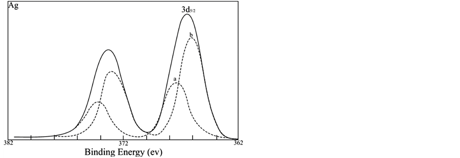
Figure 3. The XPS spectra of Ag3d for sample A (after 5 min sputtering). Solid curve: experimental spectra; dotted curve: deconvoluted spectra; The chemical states: a. Ag; b. Agn.
Table 3. The chemical states of silver.
also show that the rate of copper deposition for sample B is faster than that for sample A under the same conditions of electroless deposition.
4) Deconvolution of Ag3d XPS spectrum predicts that there must be two chemical states of silver in the image: monoatomic silver and polyatomic silver. Furthermore, no chemical shift of Ag3d at surface proves that silver at the image surface is only in a monoatomic state.
Acknowledgements
This work was supported by the National Natural Science Foundation of China (No. 21176128) and Scientific and Technological Innovation Project of Qingdao City, China (10-3-4-4-14-jch).
References
- Chandler, N. and Tyler, S.G. (1995) Ultra-Fine Feature Printed Circuits and Multi-Chip Modules. Microelectronics Journal, 26, 393-404. http://dx.doi.org/10.1016/0026-2692(95)98940-S
- Yu, A.A., Savas, T.A., Taylor, G.S., Guiseppe-Elie, A., Smith, H.I. and Stellacci, F. (2005) Supramolecular Nano-stamping: Using DNA as Movable Type. Nano Letters, 5, 1061-1064. http://dx.doi.org/10.1021/nl050495w
- Geissler, M., Wolf, H., Stutz, R., Delamarche, E., Grummt, U.W., Michel, B. and Bietsch, A. (2003) Fabrication of Metal Nanowires Using Microcontact Printing. Langmuir, 19, 6301-6311. http://dx.doi.org/10.1021/la034464x
- Riedel, W. (1991) Electroless Nickel Plating. ASM International, Metals Park, Ohio.
- Wang, T.C., Chen, B., Rubner, M.F. and Cohen, R.E. (2001) Selective Electroless Nickel Plating on Polyelectrolyte Multilayer Platforms. Langmuir, 17, 6610-6615. http://dx.doi.org/10.1021/la010755z
- Bhuvana, T., Kumar, G.V.P., Kulkarni, G.U. and Narayana, C. (2007) Carbon Assisted Electroless Gold for Surface Enhanced Raman Scattering Studies. The Journal of Physical Chemistry C, 111, 6700-6705. http://dx.doi.org/10.1021/jp070141o
- Landolt, D. (2002) Electrodeposition Science and Technology in the Last Quarter of the Twentieth Century. Journal of The Electrochemical Society, 149, S9-S20. http://dx.doi.org/10.1149/1.1469028
- Daoush, W.M., Lim, B.K., Mo, C.B., Nam, D.H. and Hong, S.H. (2009) Electrical and Mechanical Properties of Carbon Nanotube Reinforced Copper Nanocomposites Fabricated by Electroless Deposition Process. Materials Science and Engineering: A, 513-514, 247-253. http://dx.doi.org/10.1016/j.msea.2009.01.073
- Andricacos, P.C., Uzoh, C, Dukovic, J.O., Horkans, J. and Deligianni, H. (1998) Damascene Copper Electroplating for Chip Interconnections. IBM Journal of Research and Development, 42, 567-574. http://dx.doi.org/10.1147/rd.425.0567
- Bryant, R.A., Olm, M.T. and Fenton, D.E. (1995) Photographic Emulsions of Enhanced Sensitivity. US Patent No. 5728517.
- Mydlarz Z.G., and Budz J.A. and Bell E.L. (1998) Digital Imaging with High-Chloride Silver Halide Emulsions. US Patent No. 5783373.
- Shoesmith, D.W., Sunder, S., Bailey, M.G., Wallace, G.J. and Stanchell, F.W. (1983) Anodic Oxidation of Copper in Alkaline Solutions: Part IV. Nature of the Passivating Film. Journal of Electroanalytical Chemistry and Interfacial Electrochemistry, 143, 153-165. http://dx.doi.org/10.1016/S0022-0728(83)80261-7
- Yin, X., Hong, L. and Chen, B.H. (2004) Role of a Pb2+ Stabilizer in the Electroless Nickel Plating System: A Theoretical Exploration. The Journal of Physical Chemistry B, 108, 10919-10929. http://dx.doi.org/10.1021/jp036070k
- Chen, C.H., Chen, B.H. and Hong, L. (2006) Role of Cu2+ as an Additive in an Electroless Nickel-Phosphorus Plating System: A Stabilizer or a Codeposit? Chemistry of Materials, 18, 2959-2968. http://dx.doi.org/10.1021/cm0527571
- Hawn, D.D. and De-Koven, B.M. (1987) Deconvolution as a Correction for Photoelectron Inelastic Energy Losses in the Core Level XPS Spectra of Iron Oxides. Surface and Interface Analysis, 10, 63-74. http://dx.doi.org/10.1002/sia.740100203
NOTES

*Corresponding author.