Engineering
Vol. 3 No. 4 (2011) , Article ID: 4593 , 4 pages DOI:10.4236/eng.2011.34038
The Implementation of a High Efficiency Full-Bridge Converter
Department of Electrical Engineering, Dayeh University, Changhua, Taiwan (China)
E-mail: jchen@mail.dyu.edu.tw
Received December 18, 2010; revised March 3, 2011; accepted March 23, 2011
Keywords: High efficiency full-bridge converter, Switching losses, Synchronization filter
ABSTRACT
A high efficiency full-bridge converter is investigated and implemented in this paper. The measured data result from the other converter implemented by IC UCC3895 is to compare with that of the previous converter. This full-bridge converter proposed and implemented converter can obtain about 96% power efficiency in conversion procedure when compared with that of 90%, which were ever published by the conventional techniques. Apart from, the L-C resonance circuits were developed and embedded into the popular PWM (pulse width modulation) power converter, which is referred as the soft-switching, so as to down sizing the volume of the IC which can totally reduces the power losses caused in the duration of a semi-conductor switching.
1. Introduction
It is known that the “hardware switching” has become as “soft-switching” in the power electronic system, this is corresponding to the power transfer techniques has transmitted from PWM to switching schemes [1-3]. Thus, the efficiency in power system can be promoted definitely.
Recently, the technique of integrated circuit is developed so fast as to decrease the cost quickly. By the way, the related products become much diversity. Therefore, in order to satisfy huge of the specifications and/or power assumption, which could be ranged from the lowest value 1.5 V up to the highest value above 380 V [4-6]. Traditional a power supply with linear specification has the characters of lower power density, larger volume, and achieving the increasing and decreasing voltage at the output terminal by using of PWM scheme to handle the conducting time of power transistor [7-10]. In the present the techniques used to mitigate the transmission losses. The line winding loses caused at the secondary side of a high frequency transformer and the post-stage rectifier diode during the conversion interval [11]. These transmission losses are equivalent to the production of forward voltage and forward current. One who can make sense that the transmission losses occupy most of the part of all the power losses when the conversion is processing, since the increase of the loading current occurred at the output when some of the rectifier diodes applied. Therefore, it is known that the transmission losses are playing the key parameter which deteriorates the efficiency of the power circuit [12,13].
In this letter we aim in studying and implementing a power converter with high efficiency (above 96% in measuring), and the ZVS full-bridge converter IC (ISL 6754), which was developed by Intersil Company, is applied [14]. The reasons for selecting this conversion device are that it can be adopted in several field of the power supply developing, such as power for telecommunication and information, power of base station, power of file server, and even power of industry. Besides, it can either obtain null voltage between switching state when applied in the pre-stage control or it can also applied in the post-stage for controlling a transistor to act as a rectifier. Thus, by utilizing ISL6754 for both investigating the synchronization rectifier to improve the efficiency in transmission and implementing a full-bridge power converter with less 120 W to arrive at the total efficiency above 96%. The implementing results shown that the total efficiency can be reach approximate above 90% when the loading is within the interval of 120 W - 720 W without large power losses. Such a high efficiency power converter implemented with synchronization rectifier technique definitely obtains the affect of saving power. The rest of the paper is organized as follows. In Section 2 the introduction of power converter and its control techniques are presented. In Section 3 the synchronization rectifying techniques and the controlling means of ISL675 are shown. In Section 4 the implemented circuits with pull-up synchronization rectifying and full-bridge power converter are analyzed. The completed circuit systems with all the parameters are illustrated in Section 5. Some measured waveforms and data in the processes of the experiment are shown in Section 6. There is a brief conclusion drawn in Section 7.
2. The Framework and the Designed Parameters
It is known that the ZVF converter generally has much complicate structure, since it is built up by at least 4 power transistors for switching. A basic construction of such configuration is shown in Figure 1. Comparing to the configuration of a half-bridge voltage converter which is just constructed by the transistor with lower voltage, but it has to bear larger current. Inversely, the specified current can be selected in lower values but higher voltage for the transistor utilized in a push-pull converter. In words, if the advantages described previously can be combined together, then a high power converter could be implemented by the transistor with both lower voltage and smaller current, and such a circuit structure is referred as full-bridge converter. In Figure 1 the converter will stay in the state of so-called flying-wheel model in which the paired switching transistors at the same side will be turned on simultaneously, e.g. the two QA and QC at the upper arm or QB and QD at the lower arm. The null voltage happens at the state of the flying-wheel model because the primary of the transformer becomes as short circuit. In addition, a short period of delay time should be added into the signal duration as the switching state, i.e. the 4 transistors are both staying in cut-in or cut-off state, for the reason to generate resonance function in the circuit.
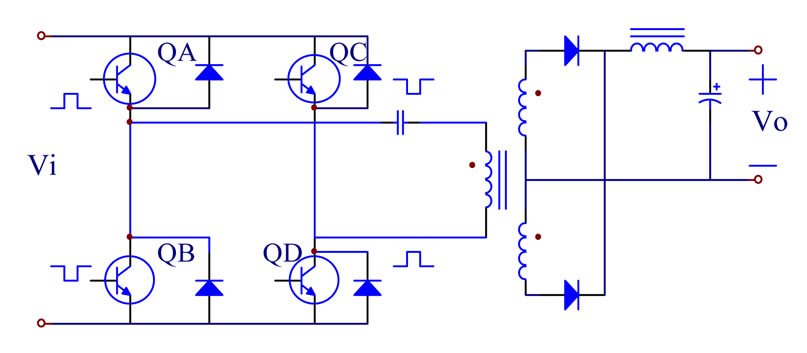
Figure 1. Zero voltage full-bridge switching converter.
The requirements for switching power transistors:
Some of the parameters of that MOSFET are listed in Table 1.
The main function of a transformer is to pull up the output voltage, to transmit the energy, and to reach at the isolation between the input and the output in the ZVS. Accordingly, the core of a transformer should not only be selected with high conduct magnetic coefficient, but the saturation flux density also should be the necessary condition. Thereafter, the larger operation space of flux can be obtained. A high frequency transformer with EEtype core is applied in the study so as to gain high capacity above 720 Watt, the operating frequency and the efficiency are about 100 KHZ and 90%, respectively.
Accordingly, the power switch has two types of driver that are direct driver and the indirect driver. Apart from, the isolate driver is then divided as magnetic isolation and photo-electronic isolation. Though the latter one has the advantages as small volume size and simple configuration, it exist bad capacity in suppressing the common mode and both lower transmission and photo coupling speed. Recently, a driver IR2110 developed by the company IR has the advantages including both photo-coupling isolation (smaller volume) and electronic magnetic isolation (faster response speed). The specifications of IR2110 can refer to [14]. The applying of isolation driver with IR2110 driver in ZVS converter is presented in Figure 2.
3. Results from Implementation and Measurement
In the implementation the former and the latter construc-
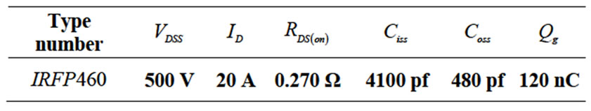
Table 1. Some important parameters of IRFP460.
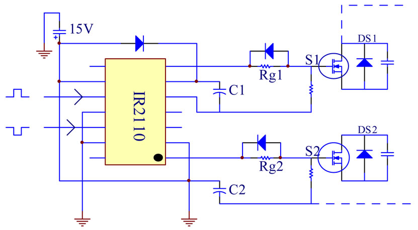
Figure 2. Isolation driver constructed with single bridge IR2110.
tion are completed with a synchronization rectifier converter IC, Intersil ISL6754, and a resonance converter IC, Texas Instruments UCC3895, respectively. Moreover, all the specifications of the two converter IC are describer as follows, input voltage ( ): DC0 V - DC300 V, output voltage (
 ): DC120 V, maximum output current (
 ): 6 A, switching frequency (fs): 100 kHz and the output power range: 120 W - 720 W.
 (a)
(a) (b)
(b)
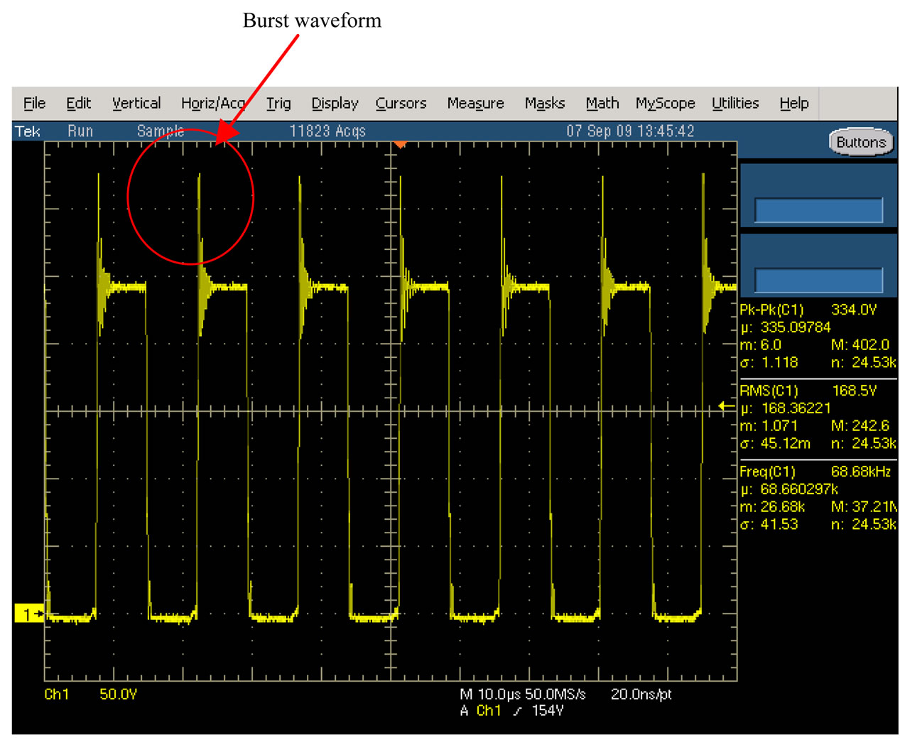
Figure 3. (a) The waveform before C49 stalled; (b) The waveform after C49 installed.
3.1. The Implemented Circuit with UCC3895
Four divisions are planned for the implemented circuit with UCC3895 including pre-stage input, post-stage output, UCC3895 switching, and driver with IR2110.
The rectifier and filter circuits are involved in the post-stage, and in which are composed by a U30D60D diode and a -type filter, respectively. It is worthy to note that the post-stage is always burn down before the  is installed. By measuring with the OSC scope, the phenomena looked for the reason that caused by the burst waveforms as shown in Figures 3(a) and 3(b). The IC UCC3895 is one controller used to modulate the phase shifter with the scheme of PWM (Pulse width modulation). The oscillator output with a UCC3895 is shown in Figure 4 in which the components
  and
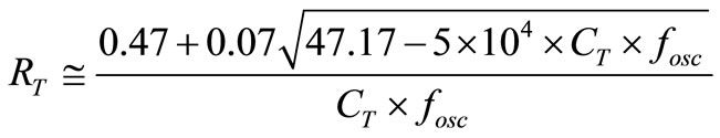
and  are constructed to adjust the operation frequency. The full implemented circuit is shown in Figure 5. The operation frequency can be determined by
 (1)
(1)
For example, the operation frequency  can be figured out by the substitution of
  and
and  into the previous equation.
Several different frequencies generate in UCC3895 are obtained and listed in Table 2 by measuring and calculating in the experimental procedure. Once the fixed frequency is decided, the values of  and
and  can to be calculated. Some referenced values of
  is listed in Table 2. Hence, the
  is also can be determined by the formula written as
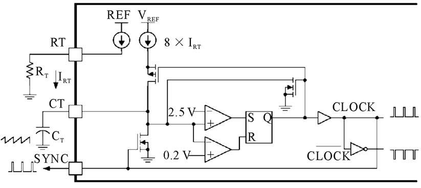
Figure 4. The oscillator circuit with UCC3895.
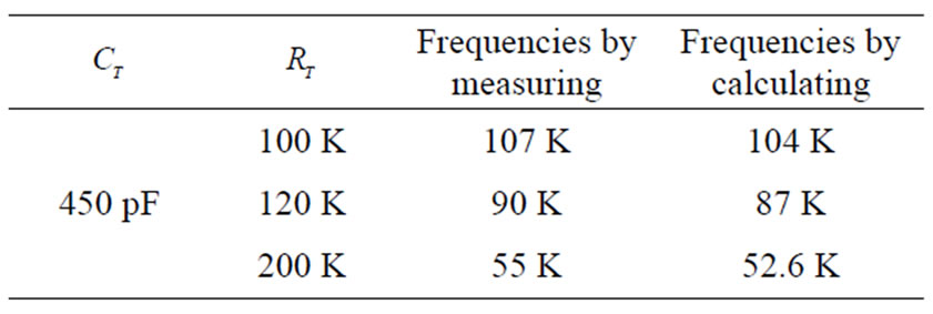
Table 2. Measured and calculated frequencies values in UCC3895.
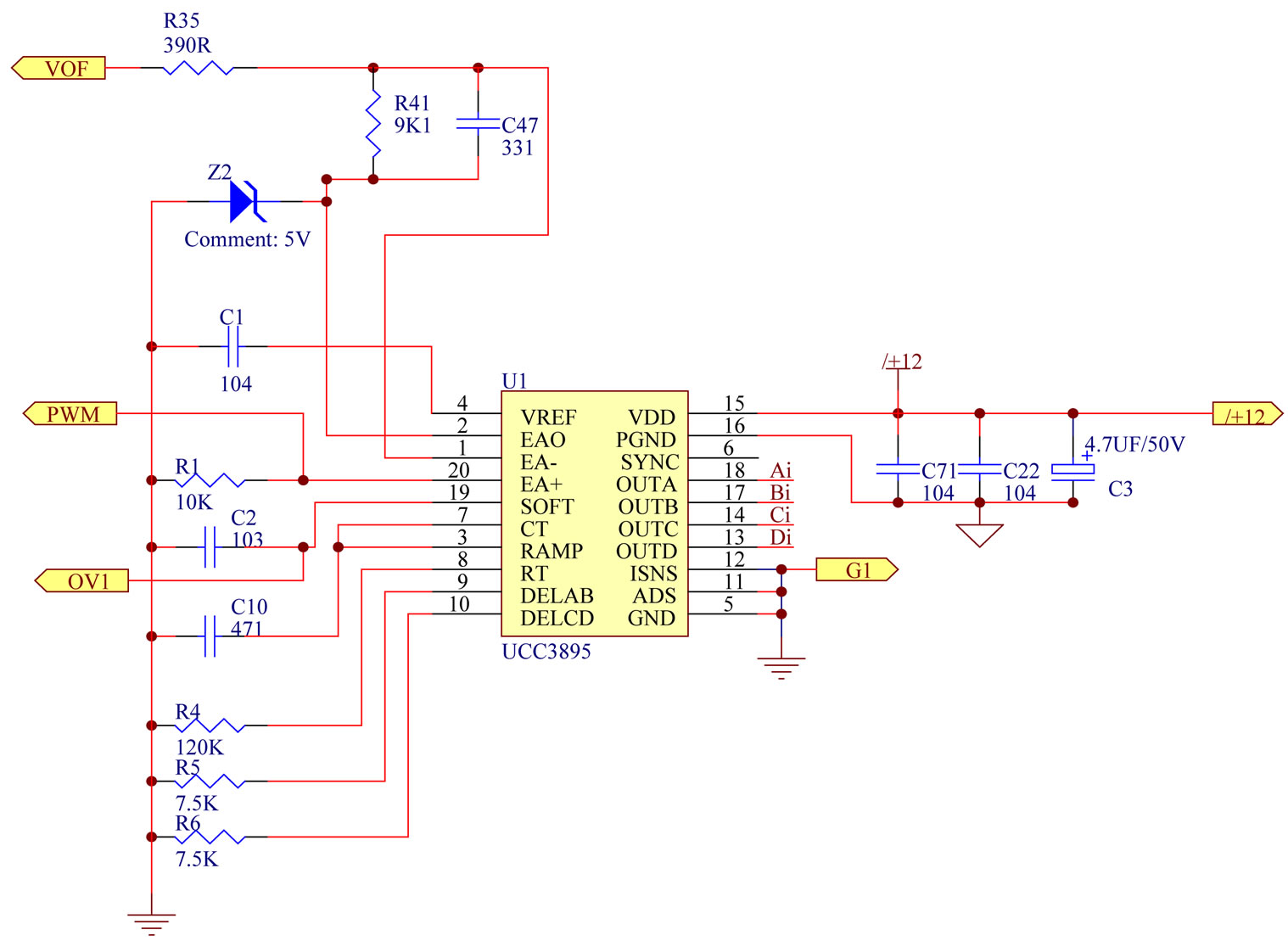
Figure 5. The completed implemented circuit.
 (2)
(2)
Four different output waveform are illustrated as OUTAi, OUTBi, OUTCi, OUTDi. It is clear to understand that the phase shift happens in OUTAi, OUTBi is caused by OUTCi, OUTDi, respectively, and this is completed (or modulated) at the pin 20 of UCC3895. However, the values of phase shift change insignificantly, see Figure 6, when try to increase the loading and the loading feedback voltage is adjusted to .
.
It is well known that a MOSFET is derived by voltage when it is playing as a switch. Thus, in this implementation the cross threshold voltage of the MOSFET in the full-bridge converter is applied to promote the input voltage from 5 V to 15 V. The main specifications of IR2110 are claimed as follows, 1) a dual input and dual output IC, 2) null dead time embedded, 3) the difference voltage can approach 500 V, 4) output voltage is 10 V - 20 V, (5) the switch time ( ) is 120 ns/94 ns.
The block diagram of the implemented driver is shown is Figure 7 in which the driver of IR2110 will notice Hi and Lo signals to ZSV converter while UCC3895 pass over the signal to. Then the full-bridge converter is comprised by these two aforementioned.
3.2. Designing ISL6754 Circuit
In this subsection including pre-stage input, post-stage output circuits and the frequency of ISL6754, and IR2110 driver are planned. The planning circuit of ISL6754 is shown in Figure 8 in which the output voltage can handled by adjusting the  voltage values, i.e. the output voltage of OUTUL, OUTUR, OUTLL, OUTLR, OUTUL, OUTURs could be controlled as periodical rectangular waveforms.
As shown in Figure 9 the waveforms of OUTUL, OUTUR, OUTLL, OUTLR are different each other and those waveform depend on the voltage value of  which is arranged in the interval 1 V - 5 V. The least energy state stays at
  in which OUTLR and OUTLL modulate OUTUR and OUTUL, respectively as shown in Figure 9.
The sequences of synchronization rectifier for ISL6754 are achieved by OUTLLN and OUTLRN. Hence, the rectifying diodes in the post-stage have to be replaced by MOSFET in order to active as a rectifier. The waveforms of OUTLLN and OUTLRN are measured and illustrated in Figure 8 with the value of . In Figure 10 the waveform of OUTUL is marked 1, waveform of OUTLR is marked 2, and waveform of OUTLLN and OUTLRN are marked 3 and 4, respectively. Alternately, in Figure 11 shows the waveforms with the condition of
 , and the shown order is same as that of Figure 10.
4. Analysis of Experimental Results
The implementation of the converter developed in this paper can be applied in high power converter. The circuitinfrusture is so-called pull-up synchronizing rectifier full-bridge converter which by using of post-stage syn-
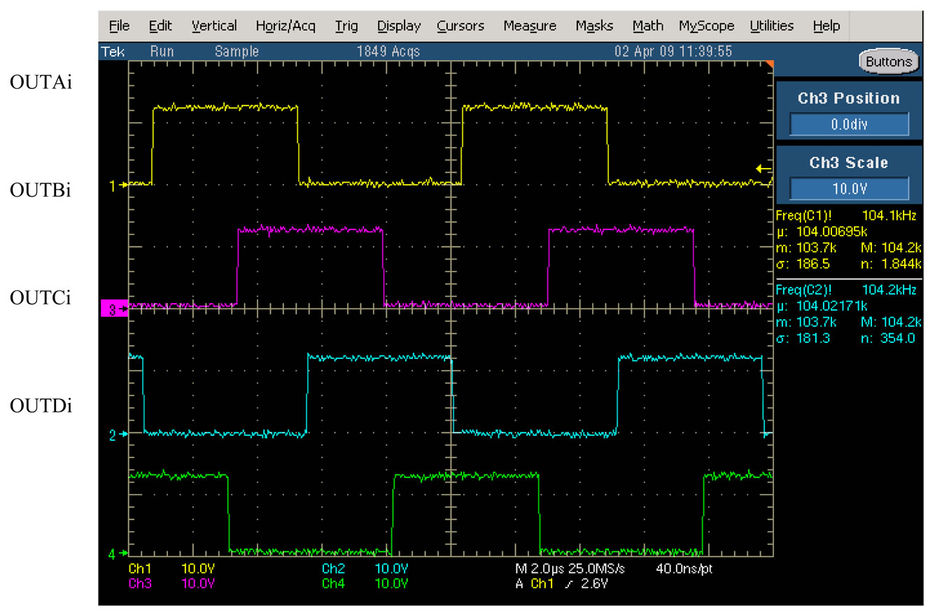
Figure 6. Four output waveforms in UCC3895 when VERR = 1 V.
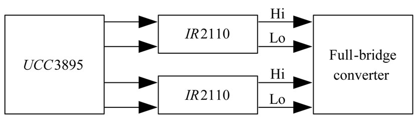
Figure 7. The block diagram of the implemented driver.
chronizing rectifier to promote the full efficiency. The adjustable output voltage,  , is obtained by the pullup converter to pull up the input voltage. A synchronizing rectifier with the unchangeable duty-cycle 50% for the main switch is built up at post-stage. The measured data of two power converters, which has the same power conversion range 120 W - 720 W, are compared and analyzed.
In the first one, the conversion switch UCC3895 is employed to set up a power switch which applies the traditional power control, and the U30D60D is adopted as a power diode set up at the post-stage. Then, the other
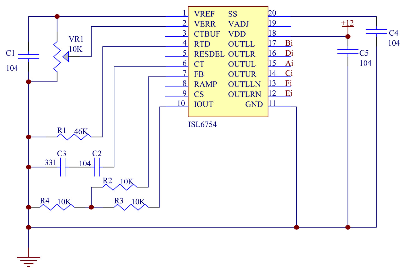
Figure 8. ISL6754 control circuit.
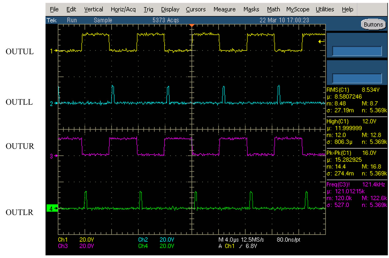
Figure 9. Four different output waveforms of ISL6754, when VERR = 1 V.
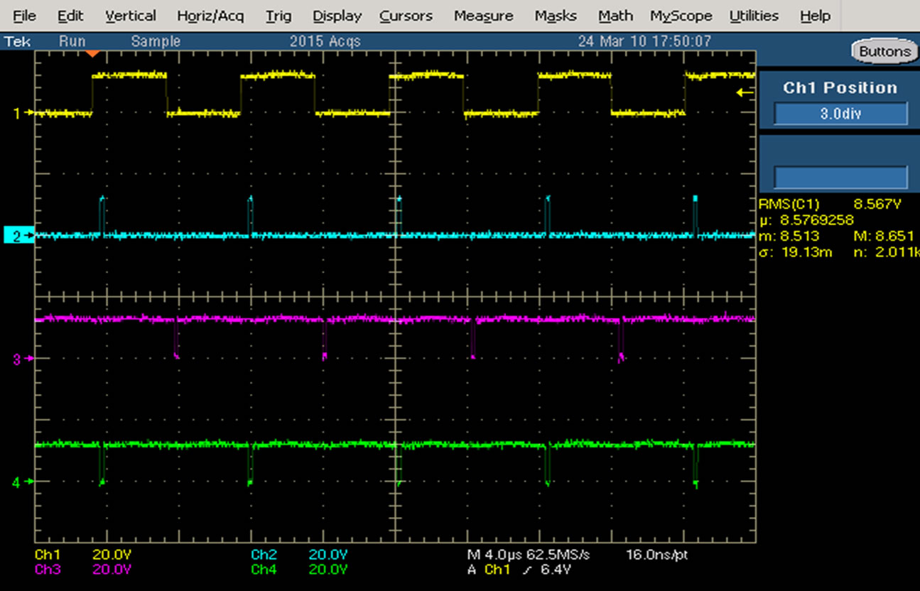
Figure 10. The 4 measured waveforms with VERR = 1 V.
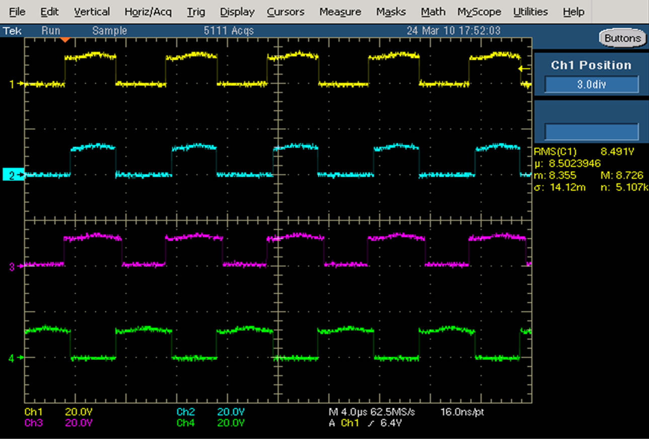
Figure 11. The 4 measured waveforms with VERR = 5 V.
one built up with Intersil ISL6754 named as ZVS power converter in which the PWM scheme is used as the power controlled switch, and the usage of MOSFET is to complete the function of synchronizing rectifier. The specifications of these two power converters are figured out as follows, input voltage ( ): DC0 V - DC300 V, output voltage (
 ): DC120 V, switching frequency (fs): 100 KHz, core of the transformer: EE55.
The resistance loading is applied to the implementation in which each branch resistance is assigned to 120 Ω/ 200 W. With the lower and higher loading, the output power may be evaluated as 123.83 W and 685.58 W, respectively. The power plots of UCC3895 are illustrated in Figure 12, it is valuable to note that the conversion efficiency is going to decrease when the power is over 240 W, and the power efficiency can’t be maintained above 90% when the power is over 600 W.
The measured data results from input voltage and output current of ISL6754 converter are listed in Table 3. In words, the power generated at output are 128.06 W
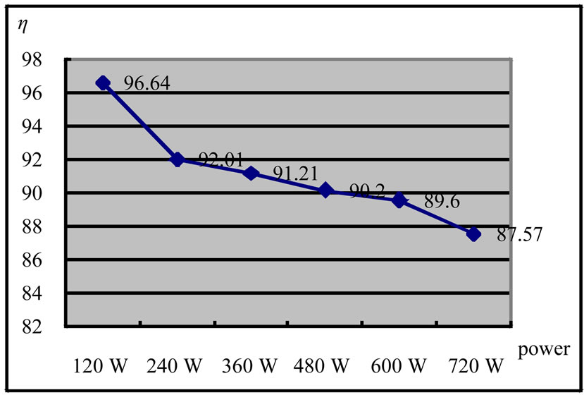
Figure 12. Power vs efficiency plots of UCC3895.
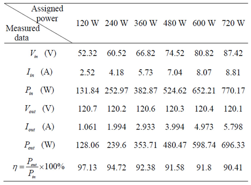
Table 3. The measured results of the implementation of ISL6754.
and 696.33 W corresponding to the lower value and higher loading value.
The comparison of power efficiency:
As the fact claimed that the conversion efficiency will decrease to below 90% when the power converted by UCC3895. Thus, the efficiency will approach to much less while the loading increase. In contrast, the conversion efficiency can be still always kept in about 90% when the power is over 600 W for ISL6754.The almost same values of power can be achieved with different IC such as UCC3895 and ISL6754 as along as the values at Pin1 and Pin2 are almost equivalent. Apart from the analysis of the power efficiency for the two different scenario are presented in Figure 13 in which Pin1 and Pout1 are assigned as input power and output power of the converter UCC3895, respectively. With the same assignment Pin2 and Pout2 indicates the input and output power of the converter ISL6754, respectively.
The range of the loading at the output is controlled in the interval 120 Ω - 20 Ω for the two converters, and the loading is held in 1 A - 6 A. It is reasonable to describe
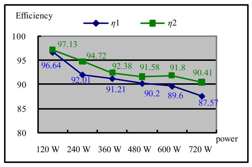
Figure 13. The comparison of efficiency for the two different circuit, where η1: UCC3895, η2: ISL6754.
some fact from Figure 13 as follow, 1) the converter equipped with ISL6754, which has the ability of synchronizing rectifier, can gain high electrical conversion, since above 90% conversion efficiency can be obtained in such an implementation, 2) both the switch on opposite side can arrive at the rules of ZVS for whichever of UCC3895 or ISL6754 converter during the switching time, and the highest power efficiency of 96.64% and 97.13% can be achieved, respectively. This fact describes that the soft switching technique definitely can be employed to improve the problem of switching power losses, 3) in terms of solving the critical issue of conduction losses caused by the rectifying diode with heavy loading, the ISL6754 converter illustrates more significant in improving the power efficiency than that of UCC3895, since the former one own the converter has the ability of synchro-nizing rectifier.
5. Conclusions and Suggestions
It is well known that the converter with a synchronizing rectifier can create high conversion efficiency just when the loading is light. Nevertheless, it should be possible to developed an alternative way which the synchronizing switch can be powered off during the loading is lower than a threshold value, and in order to break off the synchronizing switch just by using parasitic diode to establish a complete rectifier to avoid the switching losses. The volume size is also a problem for considering in cost effective direction. Finally, to joint PFC (power factor correction) technique for developing high quality power converter providing to all the consumers is one of the important targets for all the countries in the world. Certainly, one part is to promote the capacity in power supporting and the other part to increase both the power factor and the power efficiency are necessary for the best total solution.
6. REFERENCES
- S. H. Chung, S. Y. Hui and W. H. Wang, “A Zero-Current-Switching PWM Fly-Back Converter with a Simple Auxiliary Switch,” IEEE Transactions on Power Electronics, vol. 14, no. 2, March 1999, pp. 329-342. doi:10.1109/63.750187
- Y. Xi and P. K. Jain, “A Forward Converter Topology Employing a Resonant Auxiliary Circuit to Achieve Soft Switching and Power Transformer Resetting,” IEEE Transactions on Industrial Electronics, vol. 50, no. 1, February 2003, pp. 132-140.
- A. I. Pressman, “Switching Power Supply Design,” Switch-Tronix Power, Inc.
- P. Alou, J. A. Cobos, O. Garcia, R. Prieto and J. Uceda, “A New Driving Scheme for Synchronous Rectifiers: Single Winding Self-Driven Synchronous Rectification,” IEEE Transactions on Power Electronics, vol. 16, no. 6, November 2001, pp. 803-810. doi:10.1109/63.974378
- B. S. Lim, H. J. Kim and W. S. Chung, “A Self-Driven Active Clamp Forward Converter Using the Auxiliary Winding of the Power Transformer,” IEEE Transactions on Circuits and System-II: Express Briefs, vol. 51, no. 10, October 2004, pp. 549-551. doi:10.1109/TCSII.2004.836039
- M. T. Zhang, M. Jovanovic and F. C. Y. Lee, “Design Considerations and Performance Evaluations of Synchronous Rectification in Fly-Back Converters,” IEEE Transactions on Power Electronics, vol. 13, no. 3, May 1998, pp. 538-546. doi:10.1109/63.668117
- N. Yamashita, N. Murakami and T. Yachi, “Conduction Power Loss in MOSFET Synchronous Rectifier with Parallel-Connected Schottky Barrier Diode,” IEEE Transactions on Power Electronics, vol. 13, no. 4, July 1998, pp. 667-673. doi:10.1109/63.704135
- M. Jovanovic, M. T. Zhang and F. C. Lee, “Evaluation of Synchronous-Rectification Efficiency Improvement Limits in Forward Converters,” IEEE Transactions on Industrial Electronics, vol. 42. no. 4, August 1995, pp. 387- 395. doi:10.1109/41.402478
- Y. Panov and M. Jovanovic, “Design and Performance Evaluation of Low-Voltage/High-Current DC/DC OnBoard Modules,” IEEE Transactions on Power Electronics, vol. 16, no. 1, January 2001, pp. 26-33. doi:10.1109/63.903986
- B. I. Kwon, S. J. Park and S. C. Park, “Forward Converter Analysis by the Method of Coupling Electromagnetic Field with Hysteresis and Circuit Equations,” IEEE Transactions on Magnetics, vol. 36, no. 4, July 2000, pp. 1426-1430.
- Y. Xi and P. K. Jain, “A Forward Converter Topology with Independently and Precisely Regulated Multiple Outputs,” IEEE Transactions on Power Electronics, vol. 18, no. 2, March 2003, pp. 648-658.
- C.-S. Leu, “Improved Forward Topologies for DC-DC Applications with Built-In Input Filter,” Ph.D. Dissertation, Department of Electrical Engineering, Blacksburg, Virginia, 24 January 2006.
- UCC3895 Data Sheet.
- Intersil ISL6754 Data Sheet.