Materials Sciences and Applications
Vol.06 No.09(2015), Article ID:59911,9 pages
10.4236/msa.2015.69082
Fabrication of Copper Wire Using Glyoxylic Acid Copper Complex and Laser Irradiation in Air
Tomoji Ohishi*, Ryutaro Kimura
Department of Applied Chemistry, Faculty of Engineering, Shibaura Institute of Technology, Koto-ku, Japan
Email: *tooishi@sic.shibaura-it.ac.jp
Copyright © 2015 by authors and Scientific Research Publishing Inc.
This work is licensed under the Creative Commons Attribution International License (CC BY).
http://creativecommons.org/licenses/by/4.0/


Received 4 August 2015; accepted 22 September 2015; published 25 September 2015
ABSTRACT
Preparation of a glyoxylic acid copper complex and fabrication of fine copper wire by CO2 laser irradiation in air to a thin film of that complex have been investigated. Irradiating laser to the complex thin film spin-coated on a glass substrate, thin film of metallic copper was fabricated in areas that were subjected to laser irradiation in air. The thickness of this thin copper film was approx. 30 to 40 nm, and as non-irradiated areas were etched and removed by a soluble solvent of the copper complex, fine copper wire with 200 µm width was formed by laser direct patterning. The resistivity of this thin copper film depended on the irradiation intensity of the laser and was 3.0 × 10⁻⁵ Ω・cm at 12 W intensity (sweep speed: 20 mm/s). This method enables the high-speed deposition of copper wiring in air by a printing process, indicating an inexpensive and useful process for fabricating copper wiring.
Keywords:
Glyoxylic Acid Copper Complex, CO2 Laser, Fine Copper Wire, Laser Direct Patterning, Printable Electronics

1. Introduction
As electronic devices become smaller, more powerful, and more sophisticated, the development of higher densities of electrical wiring is progressing rapidly. This is creating a strong demand for the development of techniques of fabricating fine metal wires inexpensively. Conventionally, physical film formation methods in a high vacuum, such as sputtering or vacuum deposition, are mainly used in the fabrication of wiring for electronic devices. However, such methods require large-scale high-vacuum equipment and are one reason behind the increasing cost of manufacturing electronic devices.
Recently, attention has been attracted by printable electronics, in which a low-cost printing method is used to fabricate electronic devices [1] -[3] . This method is attracting attention as a revolutionary inexpensive method in the manufacture of electronic devices in that it enables the formation of films in simple equipment under normal pressure, in comparison with conventional methods using high-vacuum equipment. In the fabrication of metal wiring, it is becoming possible to make wiring by a printing method using metal particles. Although studies relating to the formation of gold and silver wiring have been reported [4] - [10] , these use a high-dispersion solution of ultrafine particles of gold or silver in the formation of films by methods such as screen printing or inkjet printing. However, gold and silver present a problem from the viewpoint of reducing costs because they are precious metals. For that reason, the fabrication of copper wiring using a dispersed solution of particles of the base metal copper is being studied [11] [12] . However, since copper oxidizes extremely easily, it is essential to process it in an inert gas, such as the synthesis of the copper particles, the fabrication and handling of their dispersion solution, and the thermal processing necessary for film curing [13] [14] . It is therefore inevitable that these fabrication processes and equipment become complicated, which is one reason for increasing costs. That is why manufacturers are anticipating the development of chemical compounds of copper sources that are stable and also inexpensive, and the development of a simple copper wiring fabrication processing technique.
The aim of our research is to develop a simpler method of fabricating copper wiring, and we have been investigating high-speed fabrication of fine wiring in air using a stable copper metal complex and laser irradiation. We have synthesized a copper complex bonded with glyoxylic acid as a ligand, and have found that laser irradiation to a film of that complex can deposit a stable metallic copper, even in air. Since the copper is deposited only on areas that are irradiated by the laser, this enables the direct patterning of copper wiring.
There have recently been reports of research in which a copper precursor is irradiated with light to form a thin copper film [15] [16] , but it is known that the type of copper salt or copper complex that is the starting material has a significant effect on the nature of a thin copper film. The glyoxylic acid used in this research has a reducing character due to its aldehyde groups, so that when it is heated, it breaks down readily to H2O, CO, and CO2 and is eliminated from the film. A copper complex that uses this glyoxylic acid as a ligand is therefore suitable for forming a thin copper film with high purity. After a film is formed by coating, using this complex solution, it is irradiated by a carbon dioxide (CO2) laser under various conditions to form a fine copper wire.
2. Experimental
2.1. Synthesis of Glyoxylic Acid Copper Complex (GACu)
A glyoxylic acid (4.5 mmol) was dissolved in 5 ml of H2O and a 10 wt% NaOH aqueous solution was added to adjust the pH to 7. To this solution, CuSO4・5H2O (4.5 mmol) dissolved in 5 ml of H2O was added. After stirring for three hours, the blue precipitates that was produced was filtered and washed by plenty of H2O. Then these blue precipitates was dried under reduced pressure. The yield was 0.50 g, giving a yield ratio of 65.7%.
2.2. Thin Film Fabrication and Laser Irradiation
A GACu 1.14 g (6.0 mmol) was dissolved in 3 ml of a 2-amino-ethanol/ethanol 1:2 mixed solvent. The solution became a uniform blue. The solution was spin-coated (rotational speed: 2000 rpm for 30 s) on a non-alkaline glass substrate (20 × 25 × 1.5 mm), then dried for 30 minutes at 50˚C to 80˚C. This film was irradiated with a laser which varied the power of a carbon dioxide laser (wavelength 10.6 µm: SUNX LP-300). The irradiation was done with the laser focus at a scan rate of 20 mm/s. After the laser irradiation, the testpiece was etched in an ethanol/H2O 1:1 mixed solvent, eliminated the non-irradiated parts, and dried.
2.3. Evaluation
To examine the molecular structure of the synthesized complex, the Fourier-transform infrared spectrum (FT-IR) (Shimadu FTIR 8400S) was measured. The thermogravimetric differential thermal analysis of the synthesized complex was measured using TG-DTA (Shimadu TGA-50) and TG-MS (RIGAKU TG8120, Shimadu GCMS- QP2010) to examine thermal properties. The crystalline structure of the thin film was measured by X-ray diffraction instrument (RIGAKU RINT-TTR III). The surface state of the thin film was observed by Scanning Electron Microscopy (SEM) (KEYENCE VE-8800). For the cross-sectional structure of the thin film, the testpiece fabricated by a focused ion beam method (FIB) was measured using Transmission Electron Microscopy (TEM) (HITACHI HF-2000). The resistivity of the thin film was measured by a four-probe method (Mitsubishi MCP-T360).
3. Results and Discussion
3.1. Synthesis of Glyoxylic Acid Copper Complex
The synthetic route of the glyoxylic acid copper complex and the copper precipitation due to the laser are shown in Figure 1. After neutralizing the glyoxylic acid with an alkali, blue crystals were precipitated by reaction with copper sulfate in a mol ratio of 1:1. The glyoxylic acid changes to hydrate formyl form in the aqueous solution. In this substance, the oxygen in the carboxylic acid group and the oxygen in the alcohol group coordinate with Cu2+ ions, to form a chelate complex with a 5-member ring. In the resulting copper complex (GACu), it is deduced that the hydrate formyl form of glyoxylic acid coordinates a one-molecule ligand and the remaining two ligand parts have bonded with H2O. CO2 laser irradiation to this complex is expected to deposit metallic copper by reductive elimination of the ligands. CO2 laser is a kind of thermo laser because the emitting wavelength of CO2 laser (10.6 μm) is the infrared light. And the synthesized Cu complex has a absorption in the infrared region. Therefore, Cu complex absorbs 10.6 μm wavelength, and then the ligand of Cu complex decomposes by the heat of CO2 laser. The detached ligands break down and are eliminated out of the film as CO2, CO, and H2O gases, so a thin copper film with high purity is fabricated.
The infrared spectrum of this complex is shown in Figure 2. OH stretching vibration was observed at 3407

Figure 1. Synthetic procedure of copper complex and copper for- mation by laser irradiation.

Figure 2. Infrared spectra of GACu complex.
cm−1 and 3512 cm−1, weak CH stretching vibration was observed in the vicinity of 2850 cm−1, antisymmetric stretching vibration of the COO of the carboxylic acid part was observed in the vicinity of 1580 cm−1, and symmetric stretching vibration of the COO was observed in the vicinity of 1444 cm−1. With this copper complex, no stretching vibration (1730 cm−1) of C=O of the formyl group of the glyoxylic acid was observed, and a comparatively strong absorption was observed at 1040 to 1130 cm−1. This absorption is considered to be C-O stretching vibration of the hydrate formyl group, which suggests that the formyl group of the glyoxylic acid was hydrated. A similar phenomenon is observed in chloral and chloral hydrate [17] [18] . Although this is observed at 1760 cm−1 with the formyl group (νC=O) of chloral, this vibration is not seen with chloral hydrate and there is comparatively strong absorption at 1105 cm−1 and 1085 cm−1 based on νC-O that has been hydrated.
Thermogravimetric differential thermal analysis (TG-DTA) done on this metal complex in air is shown in Figure 3. Large weight reductions were observed in the vicinity of 100˚C to 125˚C and in the vicinity of 180˚C to 250˚C. The overall weight reduction ratio was 54.24%, which is comparatively close to the theoretical weight reduction ratio of 58.05% that occurs when the ligands of the complex are eliminated and broken down to generate CuO. In the DTA, a endothermic peak was observed during the weight reduction in the vicinity of 100˚C to 125˚C, and a exothermic peak was observed during the weight reduction in the vicinity of 180˚C to 250˚C. The endothermic peak is associated with the elimination of H2O coordinated to the copper and it is deduced that the exothermic peak is associated with the combustion of the glyoxylic acid ligands.
We also analyzed the gases generated during the thermal analysis, using TG-MS (thermogravimetric mass spectrometry). The results of this analysis are shown in Figure 4. The gases generated during the weight reduction in the vicinity of 100˚C to 125˚C are mainly H2O (molecular weight 18), but CO (molecular weight 28) was also observed. In this temperature range, it is assumed that it is mainly the elimination of coordinated H2O molecules that occurs. This is also consistent with the DTA endothermic peak associated with the evaporation of water vapor (H2O). Gases based on H2O, CO, and CO2 were detected during the weight reduction in the vicinity of 180˚C to 250˚C. The gases emitted during this weight reduction are thought to be the gases emitted on the thermal decomposition of coordinated glyoxylic acid ligands. The DTA exothermic peak is thought to be due to the heat generated by combustion when the glyoxylic acid ligands undergo thermal decomposition. The m/z = 32 peak observed in the mass spectrometry of Figure 4 is assumed to be due to trace amounts of O2 contained in the measurement gases.
3.2. CO2 Laser Irradiation of Complex Film
The H2O coordination sites of the developed copper complex are soluble in various solvents that can easily be substituted. Solubility with respect to 2-amino-ethanol is particularly high. This is thought to be due to the 2- amino-ethanol forming new chelate complexes coordinated with copper in the oxygen sites of the alcohol group and the nitrogen of amino group. The surface states of films fabricated by heat treatment (at 500˚C) and laser processing in the copper complex film-fabrication solution and in air or in nitrogen are compared in Figure 5. When the copper complex GACu is dissolved in a mixed solvent of 2-amino-ethanol and ethanol, it becomes a

Figure 3. TG-DTA curve of GACu complex.

Figure 4. TG-MS analysis of GACu complex.
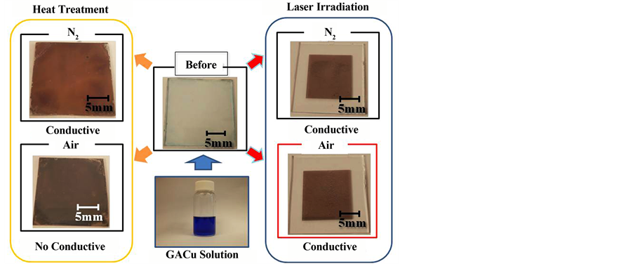
Figure 5. Surface photographs of heat-treated films and laser-irradiated films in air or N2.
blue solution, and a thin film of a pale blue copper complex is obtained by spin coating that solution.
This thin film of the copper complex subjected to heat treatment at 300˚C to 500˚C in nitrogen was converted a thin copper-colored film that exhibits conductivity, but the thin film done in air with similar processing became a thin black film that exhibits no conductivity. This thin black film is thought to be due to the oxidation of copper into copper oxide. Copper is a metal that is oxidize extremely easily, so heat treatment is usually done in an inert gas. It is thought that the thin film we have produced exhibits similar behavior. The laser-processed films, on the other hand, resulted in thin copper-colored films in both nitrogen and in air, with both exhibiting conductivity.
The X-ray diffraction spectrum shown in Figure 6 was measured in order to investigate the crystalline state of the fabricated thin films. There are different X-ray diffraction peaks for the film that was laser-processed in air, the film that was heat treated at 500˚C, and the thin Cu complex film. With the laser-irradiated film, peaks corresponding to Cu were observed at diffraction angles 2θ (Miller index) of 43.26˚ (1,1,1), 50.42˚ (2,0,0), 74.08˚ (2,2,0), and 89.80˚ (3,1,1), for films formed in air and in nitrogen, which substantially match literature values (JCPDS No.4-0836). If the lattice constant is calculated according to Bragg’s equation, using the value of 2θ = 43.26˚ in the (1,1,1) plane, the lattice plane spacing is d = 0.2091 nm and the lattice constant is 0.3622 nm. A value that was substantially the same as the lattice constant of 0.3615 nm of cubical crystal Cu was obtained. Peaks corresponding to copper oxide were not observed.

Figure 6. X-ray diffraction patterns of laser-irradiated film in air, heat- treated film at 500˚C in air and GACu complex.
On the other hand, although a Cu peak was observed in the heat-treated film that was thermally processed in nitrogen, the heat-treated film that was thermally processed in air turned black and a peak corresponding to CuO was observed.
In general, Cu is a metal that oxidizes extremely easily, so heat treatments of Cu are usually done in an inert gas. The deposition of metallic copper by laser irradiation in air is extremely interesting.
3.3. Fabrication of Fine Copper Wire by Laser Irradiation
Since copper is precipitated only on the parts irradiated by the laser, it is possible to do direct patterning of copper wiring by laser. The parts that are not irradiated by the laser remain a copper complex film, so that when the laser-irradiated substrate is etched by water/ethanol, the copper complex film of the parts that were not irradiated by the laser dissolve in the solvent and are removed, to fabricate copper wiring. Photographs of the surfaces of the copper wiring we fabricated are shown in Figure 7. When the film was irradiated while shifting the laser-irradiated parts laterally, the width of the copper wiring could be made wider. The wiring width depends on the irradiation diameter of the laser, and widths of a minimum of approximately 200 µm were obtained. Since the laser irradiation sweep speed is fast to 20 mm/s, it is possible to fabricate copper wiring rapidly.
A TEM photograph, electron diffraction patterns, and EDX analysis results of the cross-sectional structure of the fabricated copper wiring are shown in Figure 8. It is clear that the thin film is a comparatively uniform film of a thickness on the order of 30 to 40 nm, and that it has a structure in which the copper grains are connected. At the 1 and 1’ points, particles on the order of 2 nm were observed, whereas at the 2 and 2’ points a state in which large copper grains (grain diameter: approx. a few tens of nm) appeared to be connected was observed. This suggests a process of first depositing extremely fine grains of Cu by laser irradiation, then growing them into large stable Cu grains by grain growth. Peaks corresponding to metallic copper were observed by EDX analysis, showing that the fabricated thin film is metallic copper. Although a small amount of C was detected, it is not currently clear whether this is due to ligand derivatives contained in the film, or to the deposition of C used in the fabrication of the TEM testpieces. For an electron diffraction image of the film, a clear electron diffraction image is observed, showing that the Cu has crystallized. The calculation of the plane lattice spacing from a measured value (point 1) of the diffraction image shows, d1 = 0.081 nm, d2 = 0.187 nm, d3 = 0.074 nm,  d1-0-d2 = 90.2˚, and
  d1-0-d3 = 23.8˚. These values substantially match the values for cubic Cu (JCPDS No.4-0836), namely:
  = 0.081 nm, 200 = 0.181 nm,
  = 0.074 nm,
  -0-200 = 90.0˚, and
  - 0-
- 0- = 24.1˚. It was also clear from electron diffraction analysis that cubical crystal Cu was deposited.
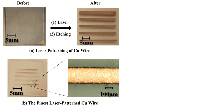
Figure 7. Laser patterning of Cu wire by etching.
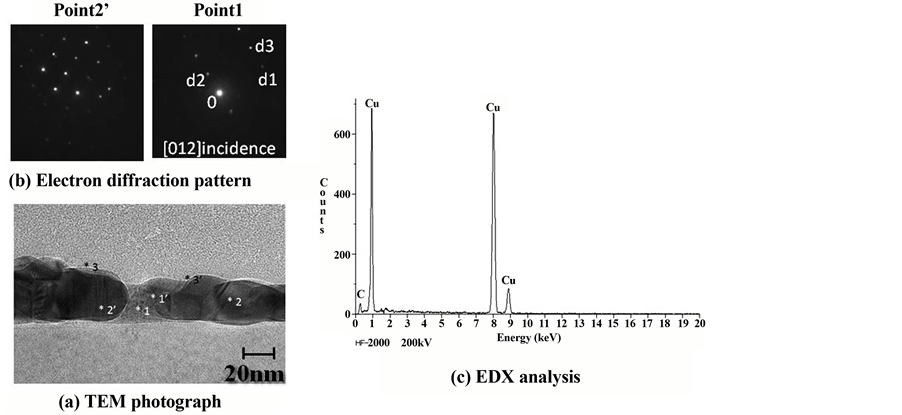
Figure 8. Cross-sectional TEM images of Cu wire. (a) TEM photograph; (b) Electron diffrac- tion pattern; (c) EDX analysis.
3.4. Effects of Laser Power on Surface State and Resistance of Cu Film
Changing the laser power, changes occurred in the resistivity and surface state of the Cu film. Changes in the resistivity and surface state when the laser irradiation power was varied are shown in Figure 9. At power intensities of up to 4 W, the conversion to Cu was insufficient, forming a film that was a mix of the metal complex film and Cu. Therefore, the resistance became insulating. At 4 W upward, conductivity appeared and resistance decreased as the power increased, reaching 3.0 × 10⁻⁵ Ω・cm at 12 W. From 13 W upward, film ablation occurred and the film peeled off, so it became insulating.
Looking at the SEM photographs of the surface states of films obtained by varying the irradiation power from 4 W to 8 W then to 12 W, there were many pores in the film at 4 W, but the numbers of pores decreased as the irradiation power increased, until a state in which the copper grains had fused together was observed at 12 W. It is assumed that the continuity of the copper grains increases and resistance decreases with increasing laser irradiation power.
The resistivity of the fabricated Cu wire has not changed after at least 3 weeks on standing in air.
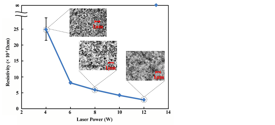
Figure 9. Relationship between laser power and resistivity and surface photographs.

Figure 10. Mechanism of Cu thin film formation by laser irradiation.
3.5. Mechanism of Copper Precipitation by Laser Irradiation
The mechanism of the formation of a thin Cu film by laser irradiation in air is shown in Figure 10. A CO2 laser with wavelength 10.6 µm is the infrared laser, which can impart heat of a high energy density to the irradiated parts locally and also instantaneously. Ligands are instantaneously eliminated and destroyed by this heat. During this time, electrons that result from the reductive elimination of the ligands are given to the Cu2+ ions which are reduced to Cu. It is assumed that, since the Cu immediately after the reduction generation has extremely small grains, its melting point is greatly reduced in comparison with metallic copper in bulk. The size effect reducing melting point is well-known to nano-metal particle [19] [20] . The fine copper grains are melted by the heat of the laser irradiation, and it is thought that they grow into more stable large grains faster than they oxidize.
With a heat treatment, on the other hand, the thermal energy is applied by convection within the entire film. For that reason, it is assumed that the fine Cu grains generated when the ligands were reductively eliminated will react immediately with oxygen in the air, to generate copper oxide.
With this method, it is possible to form fine wires of copper in air, using a stable copper complex in the materials. This makes it possible to fabricate copper wiring at high speed by laser processing, without requiring special high-vacuum apparatus. This will lead to a reduction in cost of the copper wiring fabrication processing technique.
4. Conclusion
We synthesized a glyoxylic acid copper complex and studied the fabrication of fine copper wire by CO2 laser irradiation in air to a thin film of that complex. The synthesized complex is a complex with stable glyoxylic acid forming one molecular ligand and is soluble in solvents such as amino-ethanols. Using this complex solution, a complex thin film by spin coating was formed on a glass substrate; then a thin film of metallic copper was fabricated in parts that were subjected to laser irradiation. The thickness of this thin copper film was approx. 30 to 40 nm, and since the areas (GA Cu complex) that were not irradiated by a laser were etched by a soluble solvent, it was possible to fabricate copper wiring of a minimum wiring width of 200 µm. The resistivity of this thin copper film depended on the irradiation intensity of the laser and was 3.0 × 10⁻⁵ Ω・cm at 12 W (sweep speed: 20 mm/s). This method does not require high-vacuum equipment and, because it enables the high-speed deposition of copper wiring in air by a printing process, it is thought it will be useful as an inexpensive process for fabricating copper wiring.
Cite this paper
TomojiOhishi,RyutaroKimura, (2015) Fabrication of Copper Wire Using Glyoxylic Acid Copper Complex and Laser Irradiation in Air. Materials Sciences and Applications,06,799-808. doi: 10.4236/msa.2015.69082
References
- 1. Perelaer, J., Smith, P.J., Mager, D., Soltman, D., Volkman, S.K., Subramarian, V., Korvink, J.G. and Schubert, U.S. (2010) Printed Electronics. Journal of Materials Chemistry, 20, 8446-8453.
http://dx.doi.org/10.1039/c0jm00264j - 2. Yokoyama, M. and Kamata, T. (2008) Advanced Science and Technology for Printable Organic Electronics. CMC Publishers.
- 3. Minemawari, H., Yamada, T., Matsui, H., Tsutsumi, J., Haas, S., Chiba, R., Kumai, R. and Hasegawa, T. (2011) Inkjet Printing of Single-Crystal Films. Nature, 475, 364-367.
http://dx.doi.org/10.1038/nature10313 - 4. Fukuda, K., Sekina, T., Kobayashi, Y., Takeda, Y., Shimizu, M., Yamashita, N., Kumaki, D., Itoh, M., Nagaoka, M., Toda, T., Saito, S., Kurihara, M., Sakamoto, M. and Tokita, S. (2012) Organic Integrated Circuits Using Room-Tem-perature Sintered Silver Nanoparticles as Printed Electrodes. Organic Electronics, 13, 3296-3301.
http://dx.doi.org/10.1016/j.orgel.2012.09.028 - 5. Tokuno, T., Nogi, M., Karakawa, M., Jiu, J.T.T., Nge, Y., Aso, K. and Suganuma, K. (2011) Fabrication of Silver Nanowire Transparent Electrodes at Room Temperature. Nano Research, 4, 1215-1222.
http://dx.doi.org/10.1007/s12274-011-0172-3 - 6. Hosel, M. and Krebs, F.C. (2012) Large-Scale Roll-to-Roll Photonic Sintering of Flexo Printed Silver Nanoparticle Electrodes. Journal of Materials Chemistry, 22, 15683-15688.
http://dx.doi.org/10.1039/c2jm32977h - 7. Nakamoto, M., Kashiwagi, Y. and Yamamoto, M. (2005) Synthesis and Size Regulation of Gold Nanoparticles by Controlled Thermolysis of Ammonium Gold(I) Thiolates in the Absence or Presence of Amines. Inorganica Chimica Acta, 358, 4229-4236.
http://dx.doi.org/10.1016/j.ica.2005.03.037 - 8. Suganuma, K., Sakamoto, S., Kagami, N., Wakuda, D., Kim, K.S. and Nogi, M. (2012) Low-Temperature Low-Pres-sure Die Attach with Hybrid Silver Particle Paste. Microelectronics Reliability, 52, 375-380.
http://dx.doi.org/10.1016/j.microrel.2011.07.088 - 9. Morita, T., Ide, E., Yasuda, Y., Hirose, A. and Kobayashi, K.F. (2008) Study of Bonding Technology Using Silver Nanoprticles. Japanese Journal of Applied Physics, 47, 6615.
http://dx.doi.org/10.1143/JJAP.47.6615 - 10. Perelaer, J., Abbel, R., Wtinscher, S., Jani, R., van Lammeren, T. and Schubert, U.S. (2012) Roll-to-Roll Compatible Sintering of Inkjet Printed Features by Photonic and Microwave Exposure. Advanced Materials, 24, 2620.
http://dx.doi.org/10.1002/adma.201104417 - 11. Kim, Y., Yoo, B.W., Anthony, J.E. and Park, S.K. (2012) Controlled Deposition of a High-Performance Small-Molecule Organic Single-Crystal Transistor Array by Direct Inkjet Printing. Advanced Materials, 24, 497-502.
http://dx.doi.org/10.1002/adma.201103032 - 12. Choi, Y., Lee, J.H., Kim, S.J., Yoon, D.H. and Byun, Y.H. (2012) Highly Conductive Polymer-Decorated Cu Electrode Film Printed on Glass Substrates with Novel Precursor-Based Ink and Paste. Journal of Materials Chemistry, 22, 3624.
http://dx.doi.org/10.1039/c2jm15124c - 13. Ryu, J.G., Kim, H.S. and Hahn, H.T. (2011) Reactive Sintering of Copper Nanoparticles Using Intense Pulsed Light for Printed Electronics. Journal of Electronic Materials, 40, 42-50.
http://dx.doi.org/10.1007/s11664-010-1384-0 - 14. Ishizaki, T. and Watanabe, R. (2012) A New One-Pot Method for the Synthesis of Cu Nanoparticles for Low Temperature Bonding. Journal of Materials Chemistry, 22, 25198-25206.
http://dx.doi.org/10.1039/c2jm34954j - 15. Wang, B.Y., Yoo, T.H., Song, Y.W., Lim, D.S. and Oh, Y.J. (2013) Cu Ion Ink for a Flexible Substrate and Highly Conductive Patterning by Intensive Pulsed Light Sintering. Applied Materials & Interfaces, 5, 4113-4119.
- 16. Araki, T., Sigahara, T., Jiu, J., Nagao, S., Nogi, M., Koga, H., Uchida, H., Shinozaki, K. and Suganuma, K. (2013) Cu Salt Ink Formulation for Printed Electronics Using Photonic Sintering. Langmuir, 29, 11192-11197.
http://dx.doi.org/10.1021/la402026r - 17. Nakamoto, K. (1963) Infrared Spectra of Inorganic and Coordination Compounds. John Wiley & Sons, Inc., New York.
- 18. Bellamy, L.J. (1966) Infrared Spectra of Complex Compounds. Methuen & Co, London.
- 19. Buffat, P.H. and Borrel, J.P. (1976) Size Effect on the Melting Temperature of Gold Particles. Physical Review A, 13, 2287-2298.
http://dx.doi.org/10.1103/PhysRevA.13.2287 - 20. Li, Y., Moon, K.S. and Wong, C.P. (2006) Enhancement of Electrical Property of Anisotropically Conductive Adhesives (ACAs) Joints via Low Temperature Sintering. Journal of Applied Polymer Science, 99, 1665-1673.
http://dx.doi.org/10.1002/app.22509
NOTES

*Corresponding author.