Materials Sciences and Applications
Vol.4 No.3(2013), Article ID:29540,7 pages DOI:10.4236/msa.2013.43023
Stress Analysis on Single-Crystal Diamonds by Raman Spectroscopy 3D Mapping
![]()
1Departamento de Física, Comisión Nacional de Energía Atómica, Buenos Aires, Argentina; 2Escuela de Ciencia y Tecnología, Universidad Nacional de San Martín, Buenos Aires, Argentina; 3Consejo Nacional de Investigaciones Científicas y Técnicas, Buenos Aires, Argentina.
Email: reinoso@cnea.gov.ar
Received December 5th, 2012; revised January 16th, 2013; accepted February 15th, 2013
Keywords: Diamond; Stress; Raman Spectroscopy; 3D Mapping
ABSTRACT
Results on stress analysis for single-crystal diamonds are presented. Isolated crystals were studied by Raman mapping and depth profiling techniques, using confocal microscopy. Diamonds were deposited on molybdenum and tantalum by hot filament and microwave CVD methods at growth rates between 10 and 30 μm∙h−1. Crystals from 10 to 40 μm size were examined. Local stress was evaluated by analyzing the position, broadening and splitting of the 1332 cm−1 Raman peak in a 3D mapping. For the (001) orientation, the most stressed zone was found at the center of the crystal base, close to the interface with the substrate: a Raman peak around 1340 cm−1 was measured, corresponding to a pressure c.a. 3 GPa, according to our dynamical calculations. This peak disappears few microns out of the center, suggesting that this highly concentrated stress sector was the nucleation zone of the crystal. A shifting and slight broadening of the 1332 cm−1 band was observed in the rest of the crystal. The causes of these effects are discussed: they proved not to be due to anisotropic stress but to refractive effects. Same results were found for different crystal sizes and growth rates.
1. Introduction
Diamond is one of the most promising semiconductor materials because of its outstanding mechanical, thermal and electrical properties [1,2]. Chemical vapor deposition (CVD) growth of diamond films has progressed in the last decade [3]. In order to enhance its quality, there still remains the need to reduce boundary defects and improve the intrinsic quality of the individual crystals, as it is required to decrease the production of stress around impurities and grain interfaces.
Substrate curvature, X-ray diffraction and Raman spectroscopy have been used to evaluate the internal stress of CVD and natural diamond [4-8]. In such materials, there can be high concentrations of defects, producing a change in the material density which corresponds to a variation in the average interatomic distance, affecting the phonons energy and the Raman band position. A shift and splitting of the diamond peak have been reported and associated with anisotropic stress [7,9]. However, few studies have been reported for internal stress of single crystal diamonds [10-12]. A better knowledge of the stress layout in these crystals can lead to a clearer identification of the causes of stress within continuous films.
Raman spectra are the fingerprint of carbon based materials; they allow to obtain a wide range of information about crystalline structure, atomic interactions, internal stresses, etc. Using spatially resolved Raman techniques, such as mapping or depth-profiling, the distribution of the stresses across a sample can be characterized. Confocal micro-Raman spectroscopy allows the selective acquisition of the light scattered from the focal plane, rejecting what is coming from out-of-focus areas. However, due to the mismatch in refractive index between air and the studied material, depth scale is artificially compressed and depth resolution can be worsened by orders of magnitude compared with the diffraction-limited values, about 2 μm for most of the commercial instruments [13,14]. Neglecting these effects could lead to misinterpretations of the results. Several solutions have been proposed to work out this problem, including the use of immersion objectives to reduce the refractive index mismatch and numerical corrections of the data collected by dry objectives [15,16]. However, carefully considering this effect, confocal micro-Raman spectroscopy has been used to estimate shapes and sizes of distributed particles in heterogeneous systems [17].
In this paper, we consider the influence of refractive effect in confocal micro-Raman spectroscopy to estimate local stress at different points along diamond crystals by combining the depth-profiling and x-y mapping techniques.
2. Experimental
Diamond crystals were deposited on polished molybdenum and tantalum substrates. A modified hot filament and microwave chemical vapor deposition (HFCVD and MPCVD) methods were used.
For the HFCVD method, the deposition was carried out in a stainless steel chamber. After loading the samples, the chamber was evacuated to a pressure of 10−6 mbar. During the process, methane and hydrogen were injected at a ratio of 0.002 CH4:H2 from two different nozzles, with a total gas flow of 500 sccm, up to a pressure of 20 mbar. A 0.8 mm diameter hot tungsten filament (6 V, 40 A), which acts as a cathode, was used as an electron emitter, and it was placed at 2.5 cm from the sample holder. About 200 V were initially applied between the filament and the sample holder in order to start the plasma. Afterwards, the voltage dropped to 150 V so the current densities on the sample holder were in the range of 0.3 to 0.5 A∙cm−2. Under these conditions temperature on the substrate was about 800˚C - 1000˚C: no extra heating system was required. The plasma discharge area was about 6 cm2 on the sample holder [18].
For the MPCVD method a stainless steel chamber was also used. The chamber was evacuated to an initial pressure of 10−6 mbar and then methane and hydrogen were injected at a 0.1 CH4:H2 ratio, with a total gas flow of 200 sccm (deposition pressure 60 mbar). An 850 W magnetron mounted on a wave guide was used as microwave generator. Under these conditions, temperature on the substrate was around 1200˚C.
Raman spectra were recorded using a LabRAM HR Raman system (Horiba Jobin Yvon), equipped with a confocal microscope and a charge coupled device detector (CCD). An 1800 g/mm grating and 100 μm hole results in a 2 cm−1 spectral resolution. The 514.5 nm line of an Ar+ laser is used as excitation source. A motorized x-y-z stage allows positioning the sample within 0.1 μm accuracy. A 100X objective lens was used, generating a 1.5 μm spot and a depth of focus of 4 μm was measured on a silicon wafer [13]. The laser power density over the sample was close to 4 W∙mm−2.
Isolated crystals from several samples were characterized by Raman spectroscopy. Mappings were measured by defining a 3D grid, with 2 μm steps on planes parallel to the surface (xy) and 1 μm steps between planes. Four Raman spectra were averaged for each grid point with acquisition time between 30 and 900 s; measurements from deeper planes required longer times because spectra intensity decreases due to refraction effect on the collection aperture of the confocal system [14].
Raman spectra were acquired from as-deposited diamond crystals; then they were detached from the substrate using a double-sided adhesive tape in order to measure Raman spectra over upturned crystals. For some crystals presenting an excellent adherence to molybdenum substrates, a pretreatment was required: the sample was immersed in nitric acid, rising its temperature above 100˚C, to corrode the material before using the adhesive tape.
3. Dynamical Calculations
With the aim of studying Raman diamond frequency behavior as a result of isotropic and anisotropic pressures, calculations were performed using classical lattice dynamics with a semi-empirical potential of the form proposed by Tersoff [19] and the modifications introduced in ref [20].
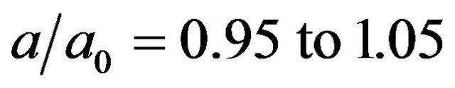
In order to test the proposed potential, the calculated frequencies for isotropic pressures were compared with experimental results [21]. In this case, the optical frequency preserves the threefold degeneracy. This frequency and the packing atomic energy has been calculated varying the cubic lattice parameter  in the range
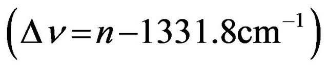
 , where a0 is the equilibrium cell parameter. An excellent agreement with experimental results was obtained for Raman frequency vs Volume per atom (Figure 1(a)). The corresponding pressure P for each compression-expansion has been calculated fitting the resulting energy vs volume curve with a quadratic polynomial; a good agreement with experimental results is obtained for pressure vs Raman frequency curve (Figure 1(b)) in the range 0 - 5 GPa [21]. Equation (1) expresses the relation between the pressure, P, and the change in diamond Raman frequency
 , in Raman spectra calculated by linear fitting data from Figure 1(b).
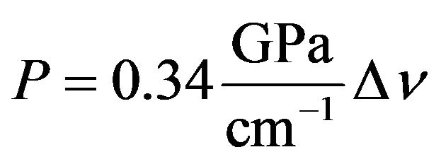 (1)
(1)
In the case of anisotropic pressures, two deformations have been considered: tetragonal (associated to a pressure along the [001]) and rhombohedral (associated to a pressure along [111]). In both cases the threefold degenerated diamond band is split in two frequencies corresponding to a longitudinal mode and a twofold degenerated transversal mode.
For the tetragonal deformation the a parameter of the cubic unit cell has been modified in the range
 . For each a value, the other parameters were relaxed, with the constraint b = c, until an energy minimum was reached. In this way, an energy vs volume curve was obtained and pressure, as described for the isotropic case, was calculated. The corresponding
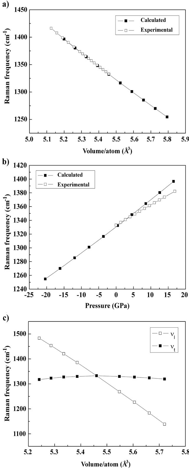
Figure 1. (a) Diamond Raman frequency vs volume per atom for isotropic deformation: calculated (black squares) and experimental (open squares) [20] data; (b) Diamond Raman frequency vs pressure for isotropic deformation: calculated (black squares) and experimental (open squares) [20] data; (c) Raman frequencies vs volume per atom for longitudinal mode νl (open squares) and transversal mode νt (black squares) calculated on anisotropically stressed diamond crystals.
frequencies for each structure were calculated as shown in Figure 1(c). It can be seen that the transversal mode remains practically unchanged, whereas the longitudinal one has strong pressure dependence. For the rhombohedral deformation, a primitive cell (a = b = c, a = β = γ = 60˚) was considered and the rhombohedral angle (α = β = γ) was modified in the range 59˚ to 61˚. For each angle value, the cell parameters were relaxed with the constraint a = b = c until an energy minimum was reached. The resulting frequencies for each structure were calculated and they show a pressure dependence similar to that described for the tetragonal case: the longitudinal mode shifts more than the transversal one.
4. Experimental Results and Discussion
Diamond crystals were grown on Mo and Ta with both methods; the growth rate was higher for MPCVD (30 μm∙h−1) than for HFCVD (10 μm∙h−1), under similar conditions. Isolated crystals with square and triangular facets, (001) and (111) orientation respectively, were deposited. Figure 2(a) shows a (001) crystal as observed under the confocal microscope coupled to the Raman spectrometer. Raman spectra on (001) surfaces showed the characteristic diamond band around 1333 cm−1 (Figure 2(b)) and a special behavior of the spectra was found for measurements at most crystals center, with the appearance of an additional peak at 1340 cm−1, but we will deal with it later. Raman spectra on (111) growth surfaces presented results very similar to those by Prawer et al. [10-12].
Mappings over xy (001) planes at the surface and at 1, 2, 3 and 5 μm of nominal depth within 10 to 40 μm size isolated crystals were made. As stated before, the depth
Figure 2. (a) Picture of (001) orientated crystal as viewed at the Raman spectrometer microscope; (b) Raman spectra obtained on the surface of a (001) diamond crystal.
scale (z) is artificially compressed due to the refraction at the air/sample interface. A nominal depth (z position from sample surface) was used to label the z planes; however, the focus depth was calculated through Everall’s model [13], indicating the focus region in which the sample was analyzed. According to this model, the mappings within the crystals correspond to the depth ranges presented in Table 1.
Figures 3 and 4 show mappings for the whole crystals, from side to side. Over the surface, Raman peak positions between 1331.5 and 1334 cm−1 were found and correlated with stress values between −0.41 and 1.29 GPa using Equation (1) as shown in Figure 3.
On each xy surface, it is readily noted that higher values are located toward the center; on the other hand, Raman peak position increases together with the nominal depth, reaching 1336 cm−1 at 3 μm. To achieve a clearer view of depth dependence, a mapping on an xz plane over a line which crosses the crystal center was performed. It can be observed as before, that Raman peak positions and pressure are higher toward the crystal base center (Figure 4).
Raman peak splitting or shift toward higher values is generally associated with the presence of compressive stress in the material, where splitting indicates the anisotropic kind [7,9]. In the present study, the central area of the crystal surface is found to be more stressed than the edges, and stress increases toward the deepest point at the middle of the crystal. It also can be noted from
Table 1. Focus depth for each nominal depth value according to Everall’s model [12].
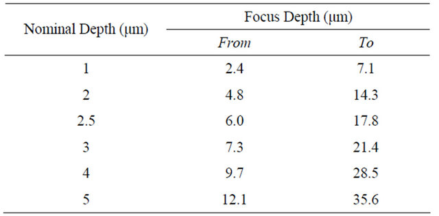
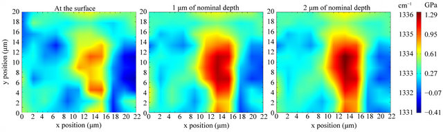
Figure 3. Mappings for diamond Raman frequency over a (001) crystal surface (left), at 1 μm (center) and at 2 μm (right) of nominal depth.
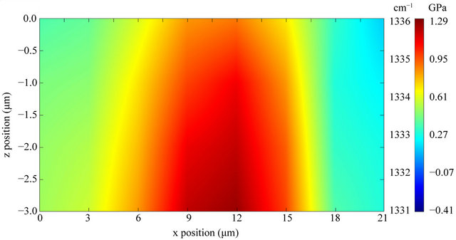
Figure 4. Mapping for diamond Raman frequency on an xz plane over a line crossing the crystal center (z axis position corresponds to nominal depth).
Figure 3, that Raman peak position varies only slightly far from crystal center. This suggests that the crystal is tightly bonded to the substrate only at the base central region, causing a high stress zone.
Furthermore, it was observed that Raman peaks width also changes across the crystals. FHMW values between 3 and 5 cm−1 were measured on the surface, reaching the higher values toward its center. On the other hand, width increases together with the nominal depth. This peak broadening could be attributed to the presence of anisotropic stress; however it must be considered that resolution decays measuring below the surface: the spectrum collects the contribution from several points at several depths with different levels of stress.
Moreover, Raman spectra from a small volume (~3 × 3 μm2, from the base up to the surface) at the center of most crystals presented a different behavior (mostly on crystals grown over molybdenum). In addition to the peak previously analyzed, a second one at 1340 cm−1 is observed. Depth profiling was made in this region, measuring at 1, 2, 2.5, 3, 4 and 5 μm of nominal depth (Figure 5(a)). At the surface, the intensity relation between these two peaks is about 3.7 and it falls to 0.5 at 4 μm of nominal depth.
A possible explanation for this band could be the presence of anisotropic stress along the crystal; however, if this was the case, an inversion of the intensity relation should not occur. On the other hand, if the anisotropic stress grows toward the crystal base, the distance between peaks should gradually increase. Moreover, according to our numerical results, the highest peak should move while the lower one should maintain its position (Figure 1(c)).
Another hypothesis is that the 1340 cm−1 band origin is a highly stressed zone located around the crystal base center. This explains the variation in the intensity relation: when measuring near the surface, the 1340 cm−1 signal comes from the focal region edge and its intensity is lower than that of the other peak. Going down, the depth of focus increases and the zone of maximum intensity of the focal region approaches the crystal base. Then, the 1340 cm−1 peak intensifies respect to the lower frequency signal. Still, the question about the stress nature (anisotropic or not) of this localized zone cannot be answered by just studying these spectra.
To answer this question, some crystals were removed from the substrate and analyzed upside down; in this position, the surface corresponds to the base of the asgrown crystal. Figure 5(b) shows a depth profiling up to 5 μm of nominal depth: a single band is observed at 1340 cm−1 at the as-grown crystal base and it shifts to lower wavenumbers going to the as-grown crystal surface. This points out that stress is not released in the detached crystals and remains around 2.6 GPa, according to our dynamical calculations (Figure 1(a)). Furthermore, no splitting was observed.
On the other hand, on crystals easily removed from Mo substrates (without nitric acid immersion), only one
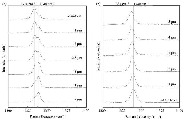
Figure 5. Raman spectra from a depth profiling on the center of: (a) as grown diamond crystal; (b) upside down diamond crystal. Nominal depth is indicated for each spectrum.
band around 1335 cm−1 was observed. This seems to indicate that less adhered crystals, which were easily removed and didn’t present the 1340 cm−1 band, are less stressed.
From the presented results and, according to Everall’s model, the splitting observed in the spectra of the asgrown crystals would be the result of dispersed light coming from different depths and not of anisotropic stress. Tens of different size crystals grown over molybdenum and tantalum by both hot filament and microwave CVD methods were studied. Similar results were obtained for all the samples.
5. Conclusion
Isolated diamond crystals of about 20 μm size were deposited and studied. The diamond Raman frequency increases towards the crystal-substrate interface center, indicating a raising in stress, as expected. At the very center of the crystal base, a special behavior was observed: an additional peak at 1340 cm−1 appeared in the best adhered crystals. Through the study of relative intensities between Raman bands as measuring deeper into the crystal and by the analysis of spectra taken from the base of the removed crystals, we concluded that stress present in our diamonds is mostly isotropic. These results were obtained for both HFCVD and MPCVD methods, for several studied isolated crystals deposited over Mo and Ta substrates despite the very different growth rates achieved for both methods (5 and 30 μm·h−1 respectively) and different crystal sizes. As has been shown, refractive effects in confocal Raman spectra could mislead the interpretations. The two peaks observed in our samples were not a splitting originated by anisotropic stress, but the sum of signals coming from different crystal zones.
6. Acknowledgements
We would like to thank M. Igarzábal and A. Zavala for technical assistance.
REFERENCES
- T. Teraji, “Chemical Vapor Deposition of Homoepitaxial Diamond Films,” Physica Status Solidi (a), Vol. 203, No. 13, 2006, pp. 3324-3357. doi:10.1002/pssa.200671408
- A. Gicquel, K. Hassouni, F. Silva and J. Achard, “CVD Diamond Films: From Growth to Applications,” Current Applied Physics, Vol. 1, No. 6, 2001, pp. 479-496. doi:10.1016/S1567-1739(01)00061-X
- M. Schwander and K. Partes, “A Review of Diamond Synthesis by CVD Processes,” Diamond and Related Materials, Vol. 20, No. 9, 2011, pp. 1287-1301. doi:10.1016/j.diamond.2011.08.005
- C. T. Kuo, C. R. Lin and H. M. Lien, “Origins of the Residual Stress in CVD Diamond Films,” Thin Solid Films, Vol. 290-291, 1996, pp. 254-259. doi:10.1016/S0040-6090(96)09016-5
- Q. H. Fan, J. Grácio and E. Pereira, “Residual Stresses in Chemical Vapour Deposited Diamond Films,” Diamond and Related Materials, Vol. 9, No. 9-10, 2000, pp. 1739- 1743. doi:10.1016/S0925-9635(00)00284-3
- J. W. Ager III and M. D. Drory, “Quantitative Measurement of Residual Stress by Raman Spectroscopy in Diamond Grown on a Ti Alloy by Chemical Vapor Deposition,” Physical Review B, Vol. 48 No. 4, 1993, pp. 2601- 2607. doi:10.1103/PhysRevB.48.2601
- H. Kagi, S. Odake, S. Fukura and D. A. Zedgenizov, “Raman Spectroscopic Estimation of Depth of Diamond Origin: Technical Developments and the Application,” Russian Geology and Geophysics, Vol. 50, No. 12, 2009, pp. 1183-1187. doi:10.1016/j.rgg.2009.11.016
- M. Mermoux, B. Marcus, A. Crisci, A. Tajani, E. Gheeraert and E. Bustarret, “Micro-Raman Scattering from Undoped and Phosphorous-Doped (111) Homoepitaxial Diamond Films: Stress Imaging of Cracks,” Journal of Applied Physics, Vol. 97, No. 4, 2005, p. 043530. doi:10.1063/1.1849828
- Q. H. Fan, A. Fernandes, E. Pereira and J. Grácio, “Evaluation of Biaxial Stress in Diamond Films,” Diamond and Related Materials, Vol. 8, No. 2-5, 1999, pp. 645-650. doi:10.1016/S0925-9635(98)00379-3
- S. A. Stuart. S. Prawer and P. S. Weiser, “Growth-Sector Dependence of Fine Structure in the First-Order Raman Diamond Line from Large Isolated Chemical-VaporDeposited Diamond Crystals,” Applied Physics Letters, Vol. 62, No. 11, 1993, pp. 1227-1229.
- S. A. Stuart, S. Prawer and P. S. Weiser, “Variation of the Raman Diamond Line Shape with Crystallographic Orientation of Isolated Chemical-Vapour-Deposited Diamond Crystals,” Diamond and Related Materials, Vol. 2, No. 5-7, 1993, pp. 753-757. doi:10.1016/0925-9635(93)90217-P
- K. W. Nugent and S. Prawer, “Confocal Raman Strain Mapping of Isolated Single CVD Diamond Crystals,” Diamond and Related Materials, Vol. 7, No. 2-5, 1998, pp. 215-221. doi:10.1016/S0925-9635(97)00212-4
- N. Everall, “Modeling and Measuring the Effect of Refraction on the Depth Resolution of Confocal Raman microscopy”, Applied Spectroscopy, Vol. 54, No. 6, 2000, pp. 773-782. doi:10.1366/0003702001950382
- K. J. Baldwin and D. N. Batchelder, “Confocal Raman Microspectroscopy through a Planar Interface,” Applied Spectroscopy, Vol. 55, No. 5, 2001, pp. 517-524. doi:10.1366/0003702011952190
- J. P. Tomba, L. M. Arzondo and J. M. Pastor, “Depth Profiling by Confocal Raman Microscopy: Semi-Empirical Modeling of the Raman Response,” Applied Spectroscopy, Vol. 61, No. 2, 2007, pp. 177-185. doi:10.1366/000370207779947477
- J. P. Tomba, M. P. Miguel and C. J. Perez, “Correction of Optical Distortions in Dry Depth Profiling with Confocal Raman Microspectroscopy,” Journal of Raman Spectroscopy, Vol. 42, No. 6, 2011, pp. 1330-1334. doi:10.1002/jrs.2843
- M. Pastorczak, M. Wiatrowski, M. Kozanecki, M. Lodzinski and J. Ulanski, “Confocal Raman Microscopy in 3-Dimensional Shape and Composition Determination of Heterogeneous Systems,” Journal of Molecular Structure, Vol. 744-747, 2005, pp. 997-1003. doi:10.1016/j.molstruc.2004.12.001
- M. Reinoso, F. Álvarez, H. Huck and E. B. Halac, “Diamond Deposited by a Direct Current Hot Cathode Plasma Discharge: Characterization and Applications,” In: T. Eisenberg and E. Schreiner, Eds., Diamonds: Properties, Synthesis and Applications, Nova Science Publishers Inc., Hauppauge, 2011, pp. 113-130.
- J. Tersoff, “Modeling Solid-State Chemistry: Interatomic Potentials for Multicomponent Systems,” Physical Review B, Vol. 39, No. 8, 1989, pp. 5566-5568. doi:10.1103/PhysRevB.39.5566
- E. Burgos, E. Halac and H. Bonadeo, “A Semi-Empirical Potential for the Statics and Dynamics of Covalent Carbon Systems,” Chemical Physics Letters, Vol. 298, No. 4- 6, 1998, pp. 273-278. doi:10.1016/S0009-2614(98)01225-1
- W. F. Sherman, “The Diamond Raman Band as a HighPressure Calibrant,” Journal of Physics C: Solid State Physics, Vol. 18, No. 30, 1985, pp. L973-L978. doi:10.1088/0022-3719/18/30/002