Circuits and Systems
Vol. 4 No. 2 (2013) , Article ID: 29858 , 8 pages DOI:10.4236/cs.2013.42021
Millimeter Wave Ring Oscillator Using Carbon Nano-Tube Field Effect Transistor in 150 GHz and Beyond
School of Electrical and Computer Engineering, Tarbiat Modares University (TMU), Tehran, Iran
Email: *davfathi@modares.ac.ir
Copyright © 2013 Davood Fathi, Baback Beig Mohammadi. This is an open access article distributed under the Creative Commons Attribution License, which permits unrestricted use, distribution, and reproduction in any medium, provided the original work is properly cited.
Received January 10, 2013; revised February 10, 2013; accepted February 17, 2013
Keywords: CNTFET; CNT Interconnect; Millimeter Wave; Ring Oscillator
ABSTRACT
Carbon Nano-Tube Field Effect Transistors (CNTFETS) are the competitor of the conventional MOSFET technology due to their higher current drive capability, ballistic transport, lesser power delay product, higher thermal stability, and so on. Based on these promising properties of CNTFETs, a CNTFET-based millimeter wave ring oscillator operating around 150 GHz and beyond is introduced here in 32 nm technology node. To prevent overestimation, the CNT interconnects between transistors are also included in simulation, which are assumed to be a single layer of ballistic metallic CNTs in parallel. For the sake of simplicity in RF design, the oscillator is based on CNTFET-based inverters. The inverters with DC gain of 87.5 dB are achieved by proper design with the non-loaded delay around 0.6 ps, which is at least one order of magnitude better than the same 32 nm MOSFET-based inverters. The oscillator’s average power consumption is as low as 40 µW with the fundamental harmonic amplitude of around −6.5 dB. These values are, based on our knowledge, for the first time reported in the literature in CNTFET-based oscillator designs. Also, on the average, the performance of the designed oscillator is 5 - 6 times better than MOSFET-based designs.
1. Introduction
Carbon nanotubes (CNTs) have shown promising electrical and mechanical performance over the conventional materials used in semiconductor industry. Electrically, CNTs are divided into two major groups: metallic and semiconducting, based on their chirality [1]. The metallic CNTs are used as interconnect in the novel integration processes [2,3] and the semiconducting ones are used in the novel semiconductor devices, beyond the conventional silicon/GaAs based technologies, like Carbon NanoTube Field Effect Transistors (CNTFETs) [4].
The large mean free path and hence, the ballistic transport characteristic of CNTs [5] with high current density capability, combining with extraordinary mobility [6] and very low shot noise [7], leads to CNTFETs with acceptable and outstanding electrical characteristics like high transit and maximum frequency [8] and inherent linearity [9].
Here, we present a high performance, low power CNTFET-based ring oscillator at 150 GHz and beyond with good THD. The amplitude of fundamental frequency of oscillation achieves around −6.5 dB which is to our knowledge 4 - 5 times better than the same MOSFETbased ring oscillators. The CNTFET used in this paper is a MOSFET-like CNTFET with gate length of 32 nm. In order to prevent overestimation of the ring oscillator performance, the CNT interconnects between CNTFETS are modeled and included in simulation, which have been arranged in a single layer of ballistic metallic CNTs.
This paper is organized as follow. Section II includes explanations on the CNTFET and its model used in our simulations. In Section III we discuss the modeling of metallic CNTs as interconnects. CNT-based inverter design and advantages over MOSFET-based inverters and its corresponding simulation results are represented in Section IV. Section V includes CNTFET-based ring oscillator design and simulation results. Finally, Section VI concludes this paper.
2. CNTFET and Its Modeling
There are several CNTFET models reported in literature [10-13]. The model used here is based on the [12,13]. This model includes all the necessary parameters needed for simulating CMOS-like CNTFETs (n-type and p-type) up to the minimum gate length of 10 nm for both large signal and small signal simulations. These parameters are quantum confinement effects on both circumferential and axial directions, acoustic, elastic and optical scattering in the channel region, screening effects of CNTs in parallel under the gate, resistive source and drain, Schottky barrier effects and the parasitic gate capacitances [12,13].
As mentioned before, the CNTFET used here is CMOSlike CNTFET. This is due to superior device parameters and fabrication feasibility of MOSFET-like CNTFETs compared with the Schotkey barrier controlled FETs [14] which makes CMOS-like CNTFETS suitable for our purpose of operating at 150 GHz and beyond.
Figure 1 shows the CMOS-like CNTFET 3D Structure. The CNTs under the gate are intrinsic and are used in such a condition that they are semiconducting. According to the analysis reported in [1], CNTs with the chirality vector (n, m) are semiconducting when n − m ≠ 3k where k is an integer. For instance, a CNT with the chirality vector (19, 0) will behave as a semiconductor.
All the CNTs simulated in this CNTFET model are assumed to be semiconducting. Of course, this is an optimistic assumption, there are so many methods developed to purify the semiconducting CNTs from metallic types. In [1], there is a method to fabricate arrays of CNTFETs without the need to separate semiconducting CNTs from metallic types, called “constructive destruction”, which is beyond our scope. The existence of metallic CNT under the gate would yield in the performance degradation through the reduction of transconductance of transistor and the increase of idle power consumption.
Despite the fact that the back-gated structure for CNTFETs is preferred to top-gate one due to simplicity in device production; we have used the top-gated topology. This is because the top-gated topology will yield higher control of gate on the channel region which enhances the transistor ability to perform better than the back-gated topology at high frequencies. Also, the structure of the circuit does not let us to utilize the back-gated topology, because the substrate that performs as the back gate is shared among all the transistors in our design.
The source and drain extensions are assumed to be
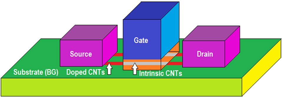
Figure 1. The three dimensional CMOS-like CNTFET structure.
made with the help of doped CNTs in parallel. This would help the device to enhance the performance of the transistor through the reduction of parasitic capacitances significantly [15]. Of course, an attention must be made that according to the lessening of mean free path of doped CNTs versus intrinsic CNTs, the length of the extended regions must be short enough in order to benefit from ballistic transport phenomena. So, there is a tradeoff between parasitic capacitance reduction and ballistic transport at the extended highly doped CNT regions.
The work function of conventional CNTs with the radius of 1 - 2 nm would be around 4.5 eV which is in a good agreement with palladium [13]. So, the palladium is used as the source and drain metal contacts. Also HfO2 with 4 nm thickness and relative permittivity of 16 has been used as the high-k gate insulator in our design.
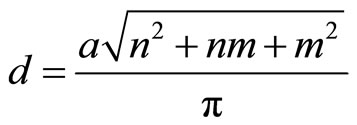
The diameter of a CNT can be calculated from
 (1)
(1)
where n and m are the indices of chirality vector (n, m) and a is the lattice constant of CNT which is around 2.46 Å. Relation (1) suggests that for a CNT with chirality vector of (19, 0) a radius of 1.5 nm must be assumed. This radius is less than the 4 nm thickness of the gate dielectric. So, there is no need to further increasing the gate insulator thickness.
The CNTs under the gate would have screening effect on each other which would degrade the CNTFET performance with increasing the number of CNTs under the gate despite the fact that increasing the number of CNTs under the gate, at first glance, must theoretically increase the transconductance of the transistor. This phenomenon will introduce an important tradeoff between the number of the CNTs under the gate and maximum CNTFET achievable performance. As a result, a distance of 4 nm is assumed between each CNT tube pairs. Further increasing of this distance will lead to undesirable increasing of the gate width which adds up more parasitic capacitances to the circuit.
We have used Stanford University CNFET HSPICE model v. 2.2.1 in simulating CNTFETs.
3. CNT Interconnect Modeling
Due to the high frequency simulation, it is necessary to include the interconnect modeling in the design. Because of the good matching between palladium source/drain contacts’ work-function and the metallic CNTs’ and according to high durability of CNTs, we choose to use CNTs as interconnect material between our logic gates described in the next section.
According to [2], due to longer mean free path of single walled carbon nanotubes versus multi walled ones, it is desirable to use SWCNTs as the interconnect material. For decreasing the resistance of the SWCNT, we may use single layer paralleled CNTs. Figure 2 shows the model for parallel CNT interconnects used in our design.
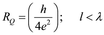
The resistance of a SWCNT is divided into two parts: Quantum resistance (RQ) and Scattering resistance (RS) [2]. The Quantum and scattering resistances can be calculated using [16]
 , (2)
, (2)
 (3)
(3)
where, λ is the mean free path, l is the length of CNT, h is the Plank’s constant, and e is the electron charge.
When the length of CNT is shorter than the mean free path, the resistance is reduced to  which is the value of quantum resistance and remains constant at this value. This condition is maintained in our design. For longer lengths, the electron scattering increases the resistance with a linear increasing behavior.
Though the value of quantum resistance is high in ballistic CNTs; the capacitance of the CNT is significantly small, making the delay of the ballistic CNT small enough for our purpose.
The capacitance also is divided into 2 parts: The electro static capacitance (CE) and quantum capacitance (CQ). The electro static capacitance between a CNT with diameter of d and the ground plane at the distance of h from the center of CNT can be calculated using (4). For a typical value of h/d, this capacitance can be approximated, with the typical value of 50 aF/µm, as [3]
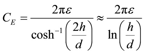 . (4)
. (4)
The quantum capacitance is in series with the electrostatic capacitance and can be calculated using [3]
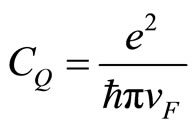 . (5)
. (5)
The value of this capacitance is around 100 aF/µmwith e as the electron charge, ħ as the Plank’s constant and vF as the Fermi velocity [3]. Also, a coupling capacitance exists between each pair of CNT interconnects, which is named CC in Figure 2. The coupling capacitance between two CNTs with diameters of d at the space of D can be calculated using [3]
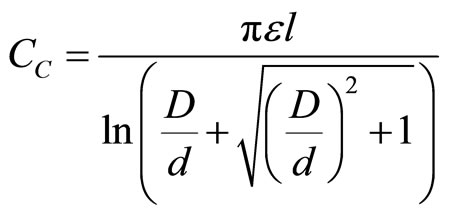 . (6)
. (6)
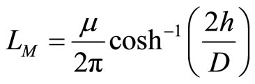
According to the previous discussion, we have assumed 4 nm space between each pair of CNT interconnects, in order to prevent the screening effect and also to decrease the coupling capacitances significantly. The total inductance of a CNT interconnect is also divided into two parts: The kinetic inductance (LK) and the magnetic inductance (LM). The kinetic inductance of a CNT can be obtained using [3]
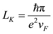 . (7)
. (7)
The value of this inductance has been assumed to be 16 nH/µm in our design. In addition to the kinetic inductance, there is a magnetic inductance in the structure of a CNT interconnect model. This inductance is small in comparison with the kinetic inductance and can be approximated to have a value of about 1 nH [3]. The exact value of the magnetic inductance can be obtained using [16]
 (8)
(8)
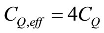
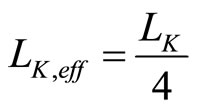
where µ is the carrier mobility and the other parameters in (8) are identical to those defined before. It should be noted here that, due to CNT’s band structure and electron’s two different spins, there are 4 conductive channels for each CNT. As a result, the effective quantum capacitance of a single CNT is four times the quantum capacitance introduced in (5). On the other hand, the effective kinetic inductance would be one quarter of the kinetic inductance in (7). So, we used CQ, eff and LK, eff in our simulations
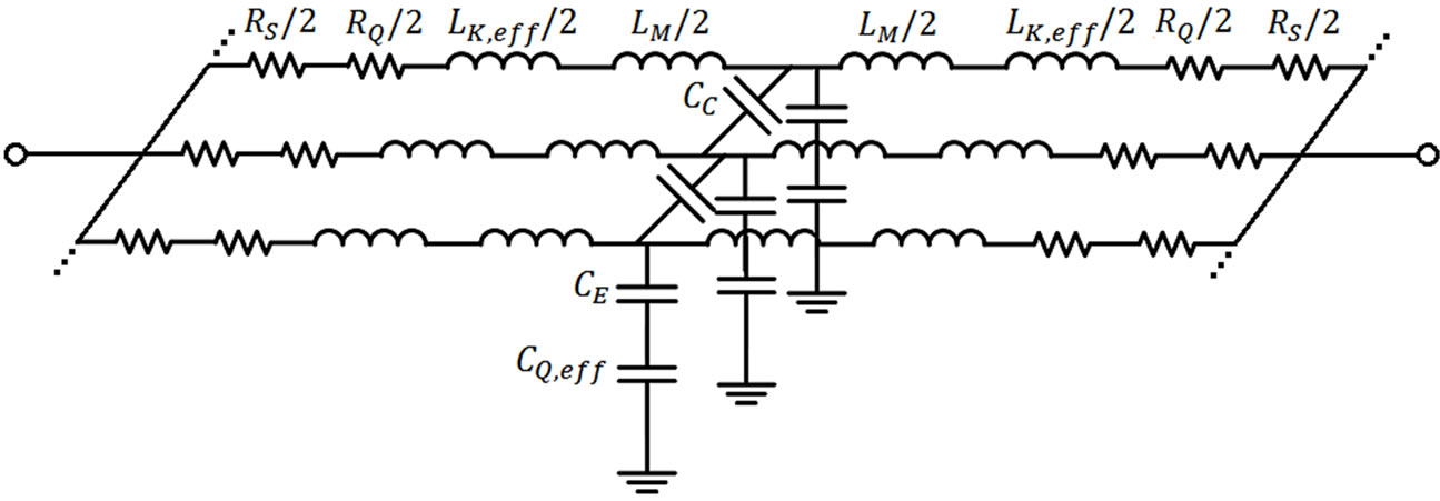
Figure 2. Parallel CNTFET interconnect model.
 , (9)
, (9)
 . (10)
4. CNTFET-Based Inverter Design
The core of the high frequency ring oscillator is based on inverters. The higher speed inverter will lead to higher frequency ring oscillator.
The high to low and low to high delays in inverters play an important role in frequency determination of an inverter based ring oscillator. Here, the total delay is a function of several parameters like the time constant of each inverter, supply voltage and the delay introduced by interconnects and connections to other gates in a real implementation.
The delay of a CNTFET based inverter is a function of CNTFET diameter under the gate. It is shown in [13] that the FO1 delay of CNTFET based inverter would be at its minimum constant value when the diameter of the CNT is around 1.4 and beyond. So, we have chosen the diameter of CNTs to be about 1.5 nm which is obtainable by a (19, 0) CNT. It must be mentioned here that for CNTs with less than 1.3 nm diameter, the higher source/ drain resistance with smaller current drive capability and hence, lower speed would be resulted [13].
There is a difference between MOSFET-based and CNTFET-based inverter design. In CMOS, there is a bulk connection for each NMOS and PMOS transistor that must be connected to proper voltages to reversely bias the p-n junctions. But here, due to physically different operational concept of CNTFETS, we have no such a connection. The back gate of the nCNTFET and pCNTFET are both the substrate and are connected to ground node in our design.
With supply voltage equal to 0.9 volts in order to prevent dielectric punch through and with proper design, the high to low and low to high delays of our CNTFETbased inverters are measured to be around 0.3 ps. The DC gain of the CNTFET-based inverter is about 87.5 dB with 5 CNTs under the gate; a value that is rarely achievable with the CMOS technology.
Figure 3 represents the voltage transfer function of a 32 nm CNTFET-based inverter and MOSFET-based inverter with different supply voltages. The significant improvement of the DC gain of the CNTFET-based inverter over MOSFET-based one is evident.
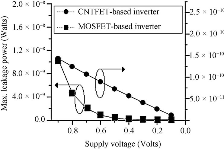
The power delay product and maximum leakage power of the CNT-based and MOSFET-based inverters are plotted versus different supply voltages and temperatures in Figures 4 and 5 respectively.
As seen from Figure 4, CNTFET-based inverter has better performance by means of maximum leakage power
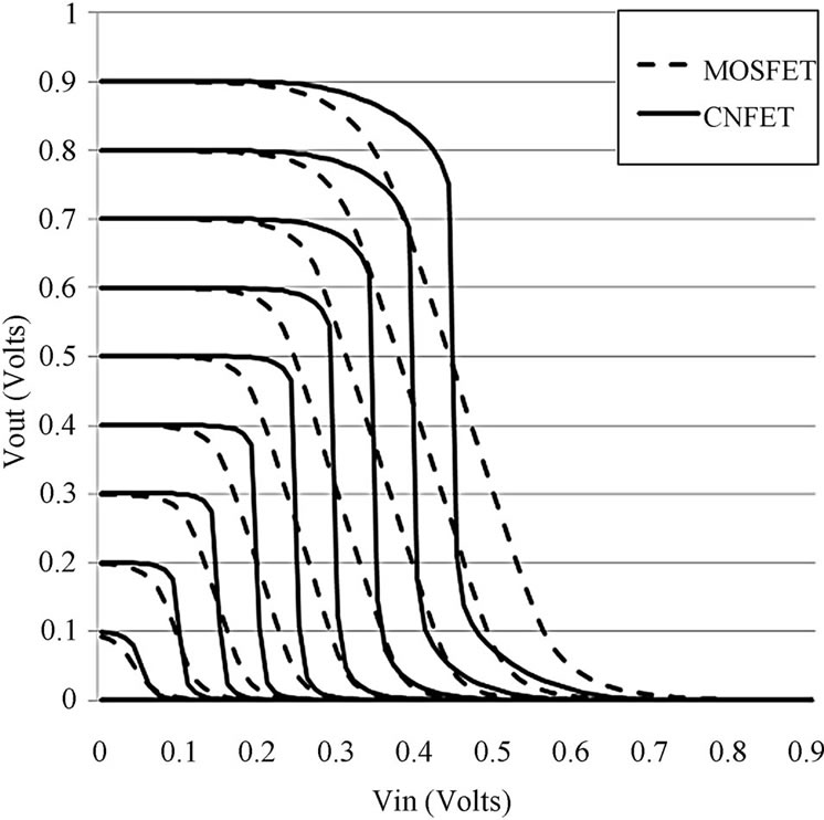
Figure 3. 32 nm CNTFET-based and CMOS based inverters’ voltage trasfer function for different supply voltages [17].
 (a)
(a)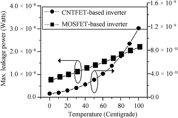 (b)
(b)
Figure 4. The maximum leakage power of CNTFET-based and MOSFET-based inverters versus (a) supply voltage and (b) temperature changes [17].
in both different supply voltages and different temperatures. On average, the overall CNTFET-based inverter’s leakage power is 40 times lesser than the MOSFETbased inverter’s.
Figure 5 illustrates the power delay product of CNTFET-based and MOSFET-based inverters with different supply voltages and in different temperatures. Again, the CNTFET-based inverter wins against MOSFET-based inverter.
Despite the fact that leakage power of CNTFET-based inverter increases exponentially with temperature, the overall leakage power on CNTFET-based inverter is about 25 times lesser than MOSFET-based inverter. Also, due to the strong stability of CNTs’ electrical characteristics against thermal variations [17], the power delay product of CNTFET-based inverter does not change sensibly in Figure 5(b).
It must be mentioned here that an overall improvement factor of at least 5 - 6 is achievable utilizing CNTFETs instead of MOSFETs by means of delay, power consumption and thermal stability [13,17].
The process variation is also important in designing and integrating reproducible electronic products. According to [17] the effective process variations in CNTFETs are different from those important in MOSFETs. The MOSFETs are 60 (26) times more sensitive to length (width) variation in gate dimensions than the CNTFETs. This is due to the fact that the current of CNTFETs is not directly related to the width and length of the channel under the gate and mostly is controlled through the number of CNTs under the gate and their chirality. Of course, this means that the purity control of CNTs under the gate is much important than dimension control in CNTFETs. It can be found that a 10% change in CNT diameter would yield a 17% change in CNTFETs current in 32 nm technology node with 0.9 V supply voltage.
5. CNTFET-Based Ring Oscillator Design
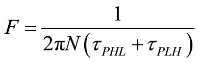
For the sake of simplicity in RF design, we have chosen the simplest inverter based ring oscillator. The ring oscillator designed here is based on the inverter-based structure including three inverters in series making a closed loop. The minimum number of three inverters is chosen to achieve the highest frequency of oscillation. The frequency of the oscillation may be predicted by
 (11)
(11)
where N is the number of inverter stages in ring,  is the high to low delay and
  is the low to high delay of each inverters having all the parasitic loads at input and output nodes.
The interconnect structure between the three inverters
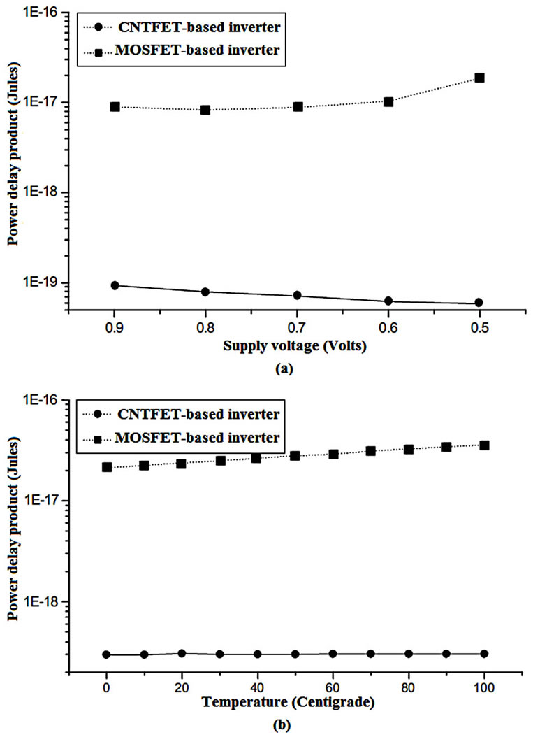
Figure 5. The power delay product of CNTFET-based and MOSFET-based inverters versus (a) supply voltage and (b) temperature changes [17].
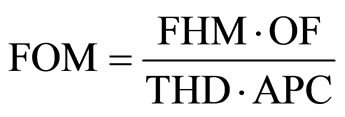
play an important role in defining the total delay of each state and hence, the maximum achievable oscillating frequency. The interconnect modeling has been discussed previously in Section III. Our suggestion is to connect the inverters as packed as possible by stretching the palladium used in the gate while closing the loop using the CNT interconnect structure, to benefit from the fixed and noiseless conductance of metallic CNTs discussed before.
As mentioned before, there are tradeoffs between different parameters like the number of metallic CNTs in a paralleled single layer set and the parasitic capacitors, the number of CNTs under the gate and CNTFET performance and delay through screening effects and gate width which will introduce more capacitors and so on. So, we have simulated different conditions to achieve the best performance of the ring oscillator by means of higher frequency and higher fundamental harmonic amplitude with lower total harmonic distortion. All the simulations are done in HSPICE simulator environment.
Table 1 represents the simulation results for different number of metallic CNTs in the single layer interconnect structure in the closing loop of ring oscillator, as shown
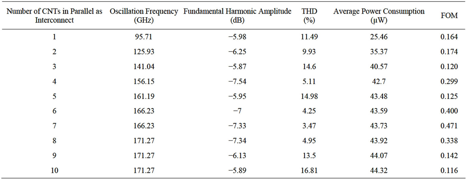
Table 1. Oscillation frequency, fundamental harmonic amplitude, total harmonic distortion, average power consumption and FOM for different number of CNTs in parallel as interconnect (gate length = 32 nanometers and number of CNTs under the gate = 5).
in Figure 6. Increasing the number of CNTs will increase the oscillation frequency, due to the increase of driving capability of inv. #3 and the reduction of interconnect resistance. But eventually, after achieving the required driving capability, increasing the number of CNTs will introduce more parasitic capacitances to the circuit and consequently, the oscillator performance will be degraded. As Figure 7 shows, based on Table 1, the optimal condition for 32 nm technology node is achieved when 7 metallic CNTs are in parallel as interconnect. The similar result will be achieved with 5 semiconducting CNTs under the gate.
The figure of merit (FOM) in Table 1 is calculated using
 (12)
(12)
where FHM is the fundamental harmonic amplitude, OF is the oscillation frequency, THD is the total harmonic distortion, and APC is the average power consumption.
As Table 2 shows, the oscillation frequency decreases as the number of CNTs under the gate increases, due to the increase of 3 factors: the parasitic capacitances, the length of interconnect, and the screening effects which are not desired in our design.
There are very few CNTFET-based ring oscillators reported in the literature. The simulation results obtained here are far beyond the results reported previously by the others in the literature. In [18], a three stage ring oscillator has been implemented, which does not benefit from the ballistic transport. Due to very large sizes of inverters, the oscillation frequency is about 220 MHz. Also, more novel oscillators reported in [19,20], have achieved the oscillation frequencies of around 80 MHz and 500 MHz respectively.
Figure 6. Connecting three inverters in chain in order to benefit from the ballistic transport phenomena in interconnect.
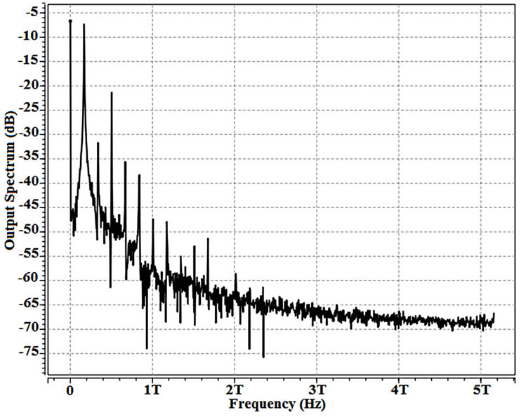
Figure 7. The output spectrum for 32 nm gate length CNTFET-based oscillator, with 5 CNTs under the gate and 7 metallic CNTs in parallel as interconnect.
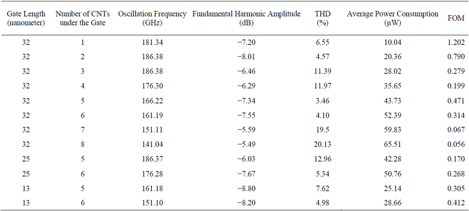
Table 2. Oscillation frequency, fundamental harmonic amplitude, total harmonic distortion, average power consumption and FOM for different number of CNTs under the gate and different gate lengths (for 7 CNTs in parallel as interconnect).
6. Conclusion
In this paper, we have designed and simulated a high performance millimeter wave ring oscillator, based on CNTFET-based inverters. The inverter and ring oscillator designed here have shown promising features versus MOSFET-based ones. The low-power consumption around 40 µ watts, the oscillation frequency of 150 GHz and beyond, the fundamental harmonic amplitude of about −6.5 dB with a good THD, above one order of magnitude improvement in the leakage power and also in the power delay product, and good thermal stability have been obtained. Also, different tradeoffs between several design parameters have been discussed in details. It should be noted that, the scope of this paper is to introduce the novel CNTFET technology and its significant benefits over the conventional MOSFET technology, in order to encourage electrical engineers to have a glance at this new promising technology.
REFERENCES
- P. Avouris, “Carbon Nanotube Electronics,” Elsevier Chemical Physics, Vol. 281, 2002, pp. 429-445.
- D. Fathi and B. Forouzandeh, “A Novel Approach for Stability Analysis in Carbon Nanotube Interconnects,” IEEE Electron Device Letters, Vol. 30, No. 5, 2009, pp. 475-477. doi:10.1109/LED.2009.2017388
- P. J. Bruke, “AC Performance of Nanoelectronics: Towards a Ballistic THz Nanotube Transistor,” Elsevier Solid-State Electronics, Vol. 48, 2004, pp. 1981-1986.
- L. Nougaret, et al., “80 GHz Field-Effect Transistors Produced Using High Purity Semiconducting Single-Walled Carbon Nanotubes,” Applied Physics Letters, Vol. 94, No. 24, 2009, Article ID: 243505. doi:10.1063/1.3155212
- A. Javey, et al., “Self-Aligned Ballistic Molecular Transistors and Electrically Parallel Nanotube Arrays,” Nano Letters, Vol. 4, No. 7, 2004, pp. 1319-1322. doi:10.1021/nl049222b
- T. Durkop, “Extraordinary Mobility in Semiconducting Carbon Nanotubes,” Nano Letters, Vol. 4, No, 1, 2003, pp. 35-39.
- P. E. Roche, et al., “Very Low Shot Noise in Carbon Nanotubes,” The European Physics Journal B, Vol. 28, No. 2, 2002, pp. 217-22. doi:10.1140/epjb/e2002-00223-9
- L. C. Castro, et al., “Extrapolated fmax for Carbon Nanotube Field-Effect Transistors,” IOP Nanotechnology, Vol. 17, No. 1, 2005, pp. 300-304. doi:10.1088/0957-4484/17/1/051
- J. E. Baumgardner, et al., “Inherent Linearity in Carbon Nanotube Filed-Effect Transistors,” Applied Physics Letters, Vol. 91, 2007.
- S. Fregonese, et al., “Computationally Efficient PhysicsBased Compact CNTFET Model for Circuit Design,” IEEE Transactions on Electron Devices, Vol. 55, No. 6, 2008, pp. 1317-1327. doi:10.1109/TED.2008.922494
- X. Yang, et al., “Modeling and Performance Investigation of the Double-Gate Carbon-Gate Nanotube Transistor,” IEEE Electron Devices Letters, Vol. 32, No. 3, 2011, pp. 231-233. doi:10.1109/LED.2010.2095826
- J. Deng, et al., “A Compact SPICE Model for CarbonNanotube Field-Effect Transistors Including Nonidealities and Its Application-Part I: Model of the Intrinsic Channel Region,” IEEE Transactions on Electron Devices, Vol. 54, No. 12, 2007, pp. 3186-3194. doi:10.1109/TED.2007.909030
- J. Deng, et al., “A Compact SPICE Model for CarbonNanotube Field-Effect Transistors Including Nonidealities and Its Application-Part II: Full Device Model and Circuit Performance Benchmarking,” IEEE Transactions on Electron Devices, Vol. 54, No. 12, 2007, pp. 3195-3205. doi:10.1109/TED.2007.909043
- J. Chen, et al., “Self-Aligned Carbon Nanotube Transistors with Charge Transfer Doping,” Applied Physics Letters, Vol. 86, 2005.
- J. Guo, et al., “Assessment of High-Frequency Performance Potential of Carbon Nanotube Transistors,” IEEE Transactions on Nanotechnology, Vol. 4, No. 6, 2005, pp. 715-721. doi:10.1109/TNANO.2005.858601
- A. Raychowdhury, et al., “A Circuit Model for Carbon Nanotube Interconnects: Comparative Study with Cu Interconnects for Scaled Technologies,” IEEE/ACM International Conference on Computer Aided Design, January 2005, pp. 237-240.
- G. Cho, et al., “Assessment of CNTFET Based Circuit Performance and Robustness to PVT Variations,” IEEE International Midwest Symposium on Circuits and Systems, Cancun, 2-5 August 2009, pp. 1106-1109.
- A. Javey, et al., “Carbon Nanotube Transistors Arrays for Multistage Complementary Logic and Ring Oscillator,” Nano Letters, Vol. 2, No. 9, 2002, pp. 929-932.
- Z. Chen, et al., “High Performance Carbon Nanotube Ring Oscillator,” Device Research Conference, February 2007, pp. 171-172.
- A. A. Pesetski, et al., “A 500 MHz Carbon Nanotube Transistor Oscillator,” Applied Physics Letters, Vol. 93, No. 24, 2008, Article ID: 243301. doi:10.1063/1.2988824
NOTES
*Corresponding author.