Circuits and Systems
Vol. 3 No. 1 (2012) , Article ID: 16606 , 6 pages DOI:10.4236/cs.2012.31004
Characterization of a Novel Low-Power SRAM Bit-Cell Structure at Deep Sub-Micron CMOS Technology for Multimedia Applications
1Department of E & CE, BT-Kumaon Engineering College, Dwarahat, India
2Department of Information Technology, VLSI Group, ABV-IIITM Gwalior, Gwalior, India
3Department of EECE, ITM University, Gurgaon, India
Email: neerajkshukla@itmindia.edu
Received September 3, 2011; revised October 3, 2011; revised October 11, 2011
Keywords: SRAM; Low-Power; Active Power; Standby Power; Gate Leakage; Sub-Threshold Leakage
ABSTRACT
To meet the increasing demands for higher performance and low-power consumption in present and future Systemson-Chips (SoCs) require a large amount of on-die/embedded memory. In Deep-Sub-Micron (DSM) technology, it is coming as challenges, e.g., leakage power, performance, data retentation, and stability issues. In this work, we have proposed a novel low-stress SRAM cell, called as IP3 SRAM bit-cell, as an integrated cell. It has a separate write sub-cell and read sub-cell, where the write sub-cell has dual role of data write and data hold. The data read sub-cell is proposed as a pMOS gated ground scheme to further reduce the read power by lowering the gate and subthreshold leakage currents. The drowsy voltage is applied to the cell when the memory is in the standby mode. Further, it utilizes the full-supply body biasing scheme while the memory is in the standby mode, to further reduce the subthreshold leakage current to reduce the overall standby power. To the best of our knowledge, this low-stress memory cell has been proposed for the first time. The proposed IP3 SRAM Cell has a significant write and read power reduction as compared to the conventional 6 T and PP SRAM cells and overall improved read stability and write ability performances. The proposed design is being simulated at VDD = 0.8 V and 0.7 V and an analysis is presented here for 0.8 V to adhere previously reported works. The other design parameters are taken from the CMOS technology available on 45 nm with tOX = 2.4 nm, Vthn = 0.224 V, and Vthp = 0.24 V at T = 27˚C.
1. Introduction
The Static Random Access Memory (SRAM) is a critical component in the modern Digital Systems-on-Chip (SoCs). As the demand for the portable multimedia rich applications is increasing, their role and need is also increasing day-by-day. As a result, SRAMs strongly impact the overall power, performance, stability and area requirements. In order to manage these constrained tradeoffs, they must be specially designed for target applications, e.g., portable multimedia products, implantable bio-medical devices, wireless sensor networks, etc. The highly power constrained systems demand more power for its active mode (read/write) operations. Also, the leakage power is coming as a big challenge in the DSM technologies, while the memory is in the standby mode, i.e., it is just retaining the data. Advancement of semiconductor technology has driven the rapid growth of very large scale integrated (VLSI) systems for increasingly broad applications almost in all sphere of life, e.g., high-end computing, consumer electronics, medical electronics, and portable multimedia products, etc. Among embedded memories, sixtransistor (6T)-based SRAM continues to play an important role in nearly all VLSI systems due to its superior speed and full compatibility with logic process technology. But as the technology scaling continues, SRAM design is facing severe challenge in maintaining sufficient cell stability margin under relentless area scaling with leakage power issues, both in dynamic and standby modes. Meanwhile, rapid expansion in mobile application, including new emerging application in sensor and medical devices, requires far more aggressive voltage scaling to meet very stringent power constraint [1]. According to the International Technology Roadmap (ITRS), 90% of the chip-area will be occupied by the memory core by 2014 [2]. This shows an increasing demand for more chips area for embedded memory with a commitment for lowpower, standby data retentation, stability, and less cell area. The power consumption in embedded SRAM memory is observed as active power (when device performing write/read switching action) and standby power (when device is in the ideal state). In the standby mode, there are several sources for the leakage current, e.g., the subthreshold current due to low threshold voltage, etc., while in the dynamic mode, the gate leakage current due to very thin gate oxides, etc., [3]. The area and power consumption by the SoC devices, occupied by static random access memory, increase largely with the technology scaling. Thus they are the critical components in both highperformance processors and handheld applications [4]. As the CMOS process technology continues to scale to the nanometer regime, process variation and leakage current of transistors become more severe, which are further aggravated by the fluctuation of the operating conditions such as the variation of the supply voltage and/or the temperature leads to a higher chance of device malfunctioning [5]. A high-performance VLSI chip also demands ever increasing on-die SRAM to meet the performance needs. This pushes the SRAM scaling towards a more concern domain in today’s VLSI design applications. The SRAM cell stability is further degraded by supply voltage scaling. The SRAM leakage power has also become a more significant component of total chip power as a large portion of the total chip transistors directly comes from on-die SRAM. Since the activity factor of a large on-die SRAM is relatively low. So, it is recommended by the researchers in the field to be more effective to put it in a power reduction mechanism dynamically, which modulates the power supply along the memory addressable unit or bank and the need for active/standby mode of operation. In this work, a novel IP3 SRAM cell structure is proposed to reduce the active and standby power, both. The proposed design has and integrated two sub-cell structure, one for write and other for read operation in the active mode. The drowsy technique [6] is utilized when the memory is in the standby mode to reduce standby power consumption. The subthreshold leakage is reduced by applying FBB scheme [7] while the cell is ideal. The read power is significantly reduced by the use of the pMOS gated structure at the read sub-cell along with the write power reduction. The data stability and data write ability, both are improved with a very less area penalty as the transistors used in the design are of minimum size.
The paper is organized as follows, the conventional 6T cell is presented in Section 2 and a brief review on the previous work is presented in Section 3. The Section 4 discusses the proposed IP3 SRAM cell structure followed by the simulation and conclusions in Section 5 and 6, respectively.
2. The Conventional 6T SRAM Bit-Cell—A Functional Approach
The Conventional SRAM (CV-SRAM) cell has Six MOS transistors (“4” nMOS and “2” nMOS), Figure 1. Unlike DRAM it doesn’t need to be refreshed as the bit is latched in. It can operate at lower supply voltages and has large noise immunity. However, the six transistors of an SRAM cell take more space than a DRAM cell made of one transistor and one capacitor thereby increasing the complexity of the cell [8].
2.1. The SRAM Bit Cell
The memory bit-cell has two CMOS inverters connected back to back (M1, M3, and M2, M4). Two more pass transistors (M5 and M6) are the access transistors controlled by the Word Line (WL), Figure 1. The cell preserves its one of two possible states “0” or “1”, as long as power is available to the bit-cell. Here, Static power dissipation is very small. Thus the cell draws current from the power supply only during switching. But ideal mode of the memory is becoming the main concern in the deep-submicron technology due to its concerns in the leakage power and data retentation at lower operating voltages.
2.2. The Operation of SRAM Bit-Cell
Although the two nMOS and pMOS transistors of SRAM memory bit-cell form a bi-stable latch, there are mainly the following three states of SRAM memory cell, the Write, Read, and Hold states.
2.2.1. Standby Operation (Hold)
When WL = “0”, M5 and M6 disconnect the cell from Bit-Lines (BL and BLB). The two cross-coupled inverters formed by M1-M4 will continue to reinforce each other as long as they are disconnected from the outside world. The current drawn in this state from the power supply is termed as standby current.
2.2.2. Data Read Operation
Read cycle starts with pre-charging BL and BLB to “1”,
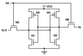
Figure 1. 6T-CMOS SRAM cell [8].
i.e., VDD. Within the memory cell M1 and M4 are ON. Asserting the word line, turns ON the M5 and M6 and the values of Q and Q’ are transferred to Bit-Lines (BL and BLB). No current flows through M6, thus M4 and M6 pull BL upto VDD, i.e., BL = “1” and BLB discharges through M1 and M5. This voltage difference is sensed and amplified to logic levels by sense amplifiers.
2.2.3. Data Write Operation
The value to be written is applied to the Bit lines. Thus to write data “0”, we assert BL = 0, BLB = “1” and to write data “1”, the BL = “1”, BLB = “0”, asserted when WL = “1”.
3. The Related Work—A Brief Review
In [8], a P3 SRAM bit-cell structure at 45nm technology has been proposed for semiconductor memories with high activity factor based applications. It makes use of the series (in-line) connected pMOS transistor to create the stacking effects for power reduction. While in standby, the stacking transistors are kept off and on during the write/read operation. The pMOS pass transistors are used to lower the gate leakage currents [9] while full-supply body-biasing scheme is used to reduce the sub-threshold leakage currents. This structure achieved a significant reduction in the dynamic and standby power in compareson with the conventional 6T SRAM cell structure, at the cost of very small area penalty and issues with SNM.
In [9], a gate leakage current reduction technique based on the pMOS pass-transistor SRAM bit-cell structure as PP-SRAM Cell has been proposed at 45 nm technology and 0.8 V supply voltage. It has lower gate leakage compared to that of the conventional SRAM cell. In order to decrease the gate leakage currents of the SRAM cell, two nMOS pass transistors, are replaced by pMOS pass transistors. In it due to the use of the pMOS pass transistors, there is an increase in the dynamic power of the cell, which is consumed during read and write operation. By keeping a view on, the use of pMOS pass transistor, may lead to performance degradation due to different mobility coefficients for the nMOS and pMOS transistors. To overcome this problem, the width of pMOS pass transistor is selected as 1.8 times of that of the nMOS that may cause an area penalty.
4. IP3 SRAM Structure—The Proposed Low-Power SRAM Bit-Cell Structure
In the novel Improved P3 (IP3) SRAM Cell, an integrated approach of two separate sub-cells (write and read) structure is proposed with a pMOS gated ground and drowsy scheme to reduce the active and standby power without losing the cells’ performance, Figure 2. The full-supply body biasing is used to further reduce the
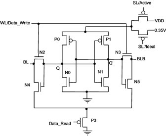
Figure 2. Proposed IP3 SRAM bit-cell.
sub-threshold leakage when the cell is in the standby mode. The data write and memory storage is being done at upper sub-cell while lower sub-cell is used for dataread operation, only. In the standby mode, the drowsy voltage (VDD = 0.35 V) is being applied to the memory to retain the data in the upper memory sub-cell at very reduced power loss. The drowsy voltage can be applied through on board power supply or through an external power supply. In the active mode of operation, the cell is supplied with VDD. In data write mode, the data read sub-cell is completely isolated from the data write subcell through BL’s and vice-versa, which further improves the cell’s stability.
4.1. Bit-Cell Analysis
A novel IP3-SRAM Cell structure with drowsy scheme and pMOS stacking with ground, e.g., pMOS gated ground, in the lower half cell half has been proposed. The basic objective for this design is to reduce the stress at 6T conventional SRAM cell in order to reduce the power consumption (active, leakage, and standby) without losing its performance. The area penalty in the new design is small as all the transistors used here are minimum sized transistors except transistor P3 which is about 1.8 times of the nMOS to meet the charge careers mobility [9] in nMOS and pMOS transistors. The proposed SRAM cell structure is comprises of two memory sub-cells, the write sub-cell (Pull Down Transistors: N0, N1; Access Transistors: N2, N3; Pull up Transistors: P0, P1) and the read-sub cell (Read Access Transistors: N4, N5; and a Gated pMOS transistor: P3). The write subcell performs the dual role, one as write data into memory and other holding the data in the memory. While writing data into the cell, the supply voltage VDD is applied before making WL/Data_Write = HIGH, and data is being passed at the BL and BLB to write in the write sub-cell. Now, WL/Data_Write put on LOW by making the BLs HIGH to latch the data in the cell. Also, while the cell is not in use, i.e., the cell in the standby, drowsy voltage 0.35 V is applied at the cell to retain the data in the cell. At this time, the stored information being available at the read sub-cell’s gate for further read access operation, without disturbing the data in the write subcell. It is a unique feature of this cell to further improve its read performance. Now, to read the data from the read sub-cell, drowsy voltage is being switched to VDD level and Data_Read signal is applied at P3 as LOW to put P3 ON and make lower sub-cell ready for read operation. Since, at this time only the read sub-cell is working, the read power reduced significantly without disturbing the stored data at the memory cell. Which further improves the cells read stability. As the write and read operations are performed in separate sub-cells, it improves the cells’ write and read performance. In the standby mode, the memory cell is kept at the low-voltage drowsy mode to ensure the data retentation in the cell. The full supply body biasing voltege, further supports in the reduced subthreshold leakage power while the cell is ideal.
4.2. Bit-Cell Operation
The active mode (data write/read) and standby mode (data hold) operation of the cell is as follows,
4.2.1. Active Mode Operation
4.2.1.1. Write Mode
Make SL/Active = 0 to apply power supply VDD at the cell. SL’/Ideal = 1, Data_Write = 1 to activate N2 and N3, and Data_Read = 1 to de-activate pMOS P3 to cut-off the lower sub-cell from the ground. Apply data to be stored in the cell at the BL and BLB to write into the upper subcell. After data write, to hold data, apply Data_Write = 0. This will cut-off the nMOS transistors N2 and N3 and cut the BL’s from the upper sub-cell. This data will also be available at the gates of the nMOS transistors N4 and N5. Apply BL and BLB as HIGH. Now, the data is latched in the upper memory sub-cell. Keep Data_Read = 1, to keep the lower sub-cell cut-off from the ground through pMOS P3.
4.2.1.2. Read Mode
Make SL/Active = 1 and SL’/Ideal = 0 to apply drowsy supply voltage of VDD = 0.35V at the upper sub-cell. Data_Write = 0 to de-activate the nMOS N2 and N3. This will disconnect the upper sub-cell from BL’s and hold data in the cell. Apply Data_Read = 0 to activate pMOS P3 and connect the lower sub-cell to the ground for its normal read operation. This will bring the lower sub-cell in the data read mode. Put the upper sub-cell at low-power drowsy mode to retain data in the cell. This stored data at Q and Q’ is also available at the gates of N4 and N5 at the lower sub-cell, so the stored data is not disturbed at the upper sub-cell, this further improves the cells’ read performance, i.e., cells’ stability improves. Now, to read the data, make BL and BLB HGH and access the stored data through the sense amplifier.
4.2.2. Standby Mode
Make SL/Active = 1, SL’/Ideal = 0 to apply drowsy voltage (VDD = 0.35V) at the cell. This will reduce the standby power of the cell. Apply Data_Write = 0 to keep the access transistors cut-off from the memory cell. Apply Data_Read = 1 to put the read sub-cell separate from the ground to reduce the standby leakage from the read sub-cell. Put the upper sub-cell at low-power drowsy mode to retain data in the cell. The lower sub-cell also cut-off from the ground through pMOS gated transistor. This will reduce the sub-threshold leakage current and will reduce the standby power leakage of the cell.
5. Simulation
The simulation work is being performed for active power write/read for data “0/1” at supply voltage of 0.8 V and at Room Temperature (RT) of 27˚C. The design parameters are, Vthn = 0.224, Vthp = 0.22V, tox = 2.4 nm and the standard nMOS and pMOS transistors to support chip fabrication process.
5.1. Performance Simulation and Analysis
5.1.1. Write Operation
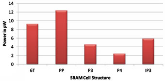
The proposed IP3 cell demands 17.65% and 41.53% less power as compared to 6T and PP cells while performing the data write operation but costs 94% and 93% more power as compared to the P4 and P3 cell, Figure 3.
5.1.2. Read Operation
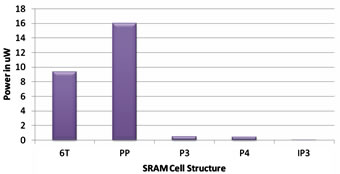
The IP3 cell is seen to be the best low-power cell among the 6T, PP, P3, P4, and P3 cells during read operation. It demands 99%, 99%, 90%, and 91% less read power as compared to the 6T, PP, P4, and P3 cell, respectively,
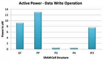
Figure 3. Active power (write) at VDD = 0.8 V.
Figure 4. Because of this feature of the proposed cell, the cell is best suited for the applications where read operation has a greater activity factor, e.g., battery powered mobile multimedia applications.
5.1.3. Standby Leakage Power
The standby leakage power, when the memory is in the idle mode, it is observed that the IP3 cell is consuming 36% and 52% less power as compared to the 6T and PP cells while it takes 59% and 23% more power to P4 and P3 cells, Figure 5.
5.1.4. Stability
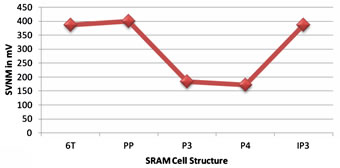
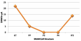
The read stability metrics, the SVNM and SINM is simulated here. The SVNM of IP3 is found no change with 6T cell while it is 55%, 52% improved with P4, P3 cells and 3% poor to PP cell. The SINM is 36% poor with 6T cell and 63%, 995, and 99% improved to PP, P4, and P3 cells, Figures 6(a) and (b). The P4 and P3 cell have poor read stability while IP3 has improved read stability.
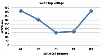
The WTV and WTI are the metrics for the write ability. The WTV for IP3 is same as that of 6T cell. The WTV for the IP3 is observed to be improved by 25%, 60%, and 62% by PP, P4, and P3 cells, Figure 7(a) The WTI is same as that of 6T and poor by 64% with PP cell while improved by almost 99% by P4, and P3 cell, Figure 7(b). The P4, and P3 cells found to be the poor read ability while the IP3 cell has marginally improved write ability.
 (a)Static Volage Noise Margin
 (b)Static Current Noise Margin
 Figure 6. Read stability: Static Voltage Noise Margin (SVNM) at VDD = 0.8 V.
 (a)
(a)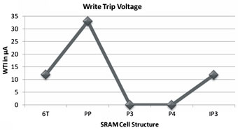 (b)
(b)
Figure 7. Write ability: Write Trip Voltage (WTV) at VDD = 0.8 V.
5.1.5. Cell Area
The cell areas for the 6T, PP, P4, and P3 cells has less area by 47%, 26%, 2%, and 2% by the IP3 cell, Figure 8. The overall performance of the cell is improved as an area tradeoff.
6. Conclusion
In the proposed IP3 SRAM cell, at one time (write/read), only half of the cell is working, this reduces the power significantly during data write and data read operations. During standby mode, an appreciable power reduction is observed. The IP3 cell has 17.65% and 41.53% improved power as compared to 6T and PP cells while performing the data write operation 94% and 93% more power as compared to the P4 and P3 cell. The IP3 cell is seen to be the best low-power cell among the 6T, PP, P3, P4, and P3 cells during read operation. It demands 99%, 99%, 90%, and 91% less read power as compared to the 6T, PP, P4, and P3 cell, respectively. The standby leakage power, of the IP3 cell is 36% and 52% less as compared to the 6T and PP cells while it 59% and 23% more than the P4 and P3 cells. The SVNM of IP3 has no change with 6T cell while it is 55%, 52% improved with P4, P3 cells and 3% poor to PP cell. The SINM is 36% poor with 6T cell and 63%, 995, and 99% improved to PP, P4, and P3 cells, i.e., it has overall improved read stability. The P4 and P3 cell have poor read stability while IP3 has improved read stability. The WTV for IP3 is same as that of 6T cell. The WTV for the IP3 is observed to be improved by 25%, 60%, and 62% by PP, P4, and P3 cells. The WTI is same as that of 6T and poor by 64% with PP cell while improved by almost 99% by P4, and P3 cell. The P4, and P3 cells found to be the poor read ability while the IP3 cell has marginally improved write ability. The cell areas for the 6T, PP, P4, and P3 cells has less area by 47%, 26%, 2%, and 2% by the IP3 cell. The overall performance of the cell is improved as an area tradeoff. Therefore, the proposed IP3 structure is good for the applications where the data is retrieve (read) operation is very high as compared to the data write, e.g., battery powered
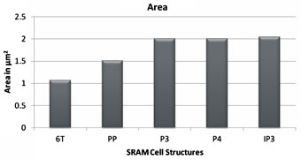
Figure 8. SRAM bit-cell area.
and portable multimedia applications. The reduction is in standby leakage power, further supports for its lowpower applications where the memory has low activity factor, i.e., to hold data when the memory is not in use at area and performance tradeoff.
7. Acknowledgements
The authors are grateful to their respective organizations for their help and support.
REFERENCES
- K. Zhang (Ed.), “Embedded Memories for Nano-Scale VLSIs,” Integrated Circuits and Systems Series, Springer, 2009.
- International Technology Roadmap for Semiconductors, 2003. http://www.publicitrs.net
- K. M. Kao, W. C. Lee, W. Liu, X. Jin, P. Su, S. K. H. Fung, J. X. An, B. Yu and C. Hu, “BSIM4 Gate Leakage Model Including Source-Drain Partition,” Proceedings of International Electron Devices Meeting, San Francisco, 10-13 December 2000, pp. 815-818. doi:10.1109/IEDM.2000.904442
- L.-J. Zhang, C. Wu, Y.-Q. Ma, J.-B. Zheng and L.-F. Mao, “Leakage Power Reduction Techniques of 55 nm SRAM Cells,” IETE Technical Review, Vol. 28, No. 2, 2011, pp. 135-145. doi:10.4103/0256-4602.78105
- C.-H. Lo and S.-Y. Huang, “P-P-N Based 10T SRAM Cell for Low-Leakage and Resilient Subthreshold Operation,” IEEE Journal of Solid-State Circuits, Vol. 46, No. 3, 2011, pp. 695-704. doi:10.1109/JSSC.2010.2102571
- K. Flautner, N. S. Kim, S. Martin, D. Blaauw and T. Mudge, “Drowsy Caches: Simple Techniques for Reducing Leakage Power,” Proceedings of 29th Annual International Symposium on Computer Architecture, Anchorage, 25-29 May 2002, pp. 148-157. doi:10.1109/ISCA.2002.1003572
- C. H. Kim, J.-J. Kim, S. Mukhopadhyay and K. Roy, “A Forward Body-Biased Low-Leakage SRAM Cache: Device, Circuit and Architecture Considerations,” IEEE Transaction on Very Large Scale Integration (VLSI) Systems, Vol. 13, No. 3, 2005, pp. 349-357.
- N. Kr. Shukla, R. K. Singh and M. Pattanaik, “A Novel Approach to Reduce the Gate and Sub-threshold Leakage in a Conventional SRAM Bit-Cell Structure at Deep-Sub Micron CMOS Technology,” International Journal of Computer Applications (IJCA), Vol. 23, No. 7, 2011, pp. 23-28.
- G. Razavipour, A. Afzali-Kusha and M. Pedram, “Design and Analysis of Two Low-Power SRAM Cell Structures,” IEEE Transaction on Very Large Scale Integration (VLSI) Systems, Vol. 17, No. 10, 2009, pp. 1551- 1555.