Journal of Modern Physics
Vol.07 No.15(2016), Article ID:71863,20 pages
10.4236/jmp.2016.715177
Fowler-Nordheim Tunneling, Photovoltaic Applications and New Band Structure Models of Electroconductive a-CNx:H Films Formed by Supermagnetron Plasma CVD
Haruhisa Kinoshita
Department of Electrical and Electronic Engineering, Graduate School of Engineering, Shizuoka University, Hamamatsu, Japan

Copyright © 2016 by author and Scientific Research Publishing Inc.
This work is licensed under the Creative Commons Attribution International License (CC BY 4.0).
http://creativecommons.org/licenses/by/4.0/


Received: October 6, 2016; Accepted: November 6, 2016; Published: November 9, 2016
ABSTRACT
Hydrogenated amorphous carbon nitride (a-CNx:H) films were formed on Al films deposited on Si or glass (SiO2) substrates, using pulsed radio frequency (PRF) supermagnetron plasma (SMP) chemical vapor deposition (CVD) with N2/i-C4H10 mixed gases. a-CNx:H films were grown under the upper and lower electrode RF powers (13.56 MHz) of continuous and pulsed conditions, respectively, which showed low band gap of about 0.7 eV. a-CNx:H films deposited on the Al/Si or Al/SiO2 substrates showed same low threshold emission electric field (ETH) of 12 V/μm. Multiple layer of Al or ITO (anode)/50nm-SiO2/a-CNx:H/Al (cathode)/Si structures showed Fowler-Nordheim (FN) electron tunneling effect in both forward and reverse current directions. 12.5 nm a-CNx:H film on p-Si substrate showed a photoelectric conversion. Energy band structure and electron conduction models were proposed for the active states of both the field emission and FN tunneling devices and photovoltaic cells.
Keywords:
Supermagnetron Plasma, Chemical Vapor Deposition, Amorphous Carbon Nitride, Energy Band, Electron Conduction, Field Emission, FN Tunneling, Photovoltaic Cell

1. Introduction
Hydrogenated amorphous carbon (a-C:H) films attract interest because their properties are suited to opto-electronic and vacuum microelectronic devices, including light emission diodes, photovoltaic cells and field electron emission devices [1] - [10] . In these films, both the optical and electrical properties can be modified by nitrogen doping; i.e., they are usually regarded as hydrogenated amorphous carbon nitride (a-CNx:H) films [11] - [20] . a-CNx:H films sometimes show high electroconductivity. Management of the substrate temperature and the intrinsic compressive stress of the films are important factors in the electronic device fabrication. In the continuous discharge of SMP for CVD, the surface temperature of the substrate is easily increased to more than 200˚C by applying RF power [19] , which causes the films to peel off from the wafers due to the high intrinsic compressive stress in these films [20] .
To suppress substrate heating resulting from the bombardment of high-energy ions, periodic plasma deposition has been found to be effective [21] . Several studies have shown PRF plasma CVD to be effective for the deposition of low-residual-stress a-CNx:H films [21] [22] [23] . Low-residual-stress films might be effective for use in electronic devices, such as vacuum field emitters and photovoltaic cells. Continuous RF SMP has been used to deposit electroconductive a-CNx:H films with a lower field- emission threshold of 9 - 12 V/μm in spite of its high deposition-wafer temperature [24] [25] [26] . Reduction of the wafer temperature using PRF SMP enables to use low melting substrates such as Al for the fabrication of a-CNx:H field emitters [27] , because of the decreased degradation of the interface state between the substrate and the grown electroconductive a-CNx:H film.
a-CNx:H films have been applied to selective transport electrodes of photoelectrons [9] [10] . Conventional silicon- or compound-semiconductor-based photovoltaic cells (PVCs) always utilize p-n junctions for the separation of photo-generated carriers, including Au/carbon material/Si PVCs [28] . In the PVCs, carbon materials have been used to generate electron-hole pairs and make photoconduction of carriers under light irradiation. However, a-CNx:H film which was fabricated by using SMP CVD has been functioned as a selective transport electrode of electrons. Hence, the film showed the charge separation of photo-generated carriers [9] [10] . The fact is that the a-CNx:H films (25 nm thickness) have shown no photoconductions under light irradiation. This difference is caused by the film deposition method. By another report, a-C:H and a-CNx:H fabricated by using conventional CVD method showed more than ten orders of magnitude difference in room-temperature conductivity depending on the deposition method used [29] . The proportion of sp2 hybridized carbon atoms and the size of their clusters determine the optical band gap and produce a significant influence on the electrical transport and Fermi level as well.
In this study, we deposited a-CNx:H films using PRF plasma modulated under a 2.5-kHz frequency. The film properties were investigated under constant upper- electrode rf power (UPRF) of 100 W and pulsed lower-electrode rf power (LORF) of 0 - 800 W, i.e. 100/0 - 800 W. These a-CNx:H films were applied to the three kinds of a-CNx:H/Al field emission, Al or ITO/SiO2/a-CNx:H/Al FN electron tunneling and a-CNx:H/p-Si photovoltaic devices. By the measurements of their I-V characteristics, the electroconductive characteristics of a-CNx:H films were evaluated. For the analysis of electron conduction in these devices, I proposed a band model of a-CNx:H film formed at 100/800W, and was able to successfully explain the electron conduction behaviors in these devices.
2. Experimental Procedures
In this experiment, a SMP CVD apparatus (Samco SMPD-10, Figure 1) was used to deposit a-CNx:H films. One of the RF power sources (lower electrode) was modulated by controlling the RF amplitude using a pulse generator, while the other was constant; both power sources had the same RF frequency. The two RF powers (constant and pulsed) were applied to two electrodes inserted into a grounded metal chamber. The upper electrode was covered with a graphite plate to prevent sputtering on the metal electrode surface. The phase difference between the two RF voltages was approximately 180˚ under a control-of-phase shifter to obtain both the maximum plasma density [30] [31] [32] and deposition rate. In addition, a rotating magnetic field (approximately 80 G) was applied parallel to the two electrode surfaces. The lower electrode (substrate holder) was heated to 100˚C during film deposition.
For film deposition, i-C4H10 (50 sccm) and N2 (120 sccm) gases were used, and the gas pressure was controlled to be 4 Pa. Profilometry (ULVAC DECTAK-3) was used to measure film thickness. Using optical absorption data measured with a UV/Vis/NIR spectrometer (Shimadzu UV-3100PC), the optical band gap was estimated from the Tauc plot based on the relation (αE)1/2 = A(E − EG), where A is a constant, α is the absorption coefficient, E is the photon energy, and EG is the optical band gap [33] . The refractive index of the a-CNx:H film deposited on the Si wafer was measured by ellipsometry (Mizojiri Optical DHA-OLXS; wavelength 632.8 nm). The bonding configurations of a-CNx:H were measured using a Fourier transform infrared (FTIR) spectrometer (JIR WINSPEC-50). The thickness of the a-CNx:H film for FTIR analysis was controlled to be about 500 nm for all samples. Film hardness was evaluated using a dynamic ultra- micro-hardness tester (Shimadzu DUH-W201). The surface morphology of the sample was measured using atomic force microscopy (AFM) (Seiko Instruments SPI3800).
3. Results
We used a PRF SMP CVD apparatus under RF power modulated by a 2.5-kHz pulse
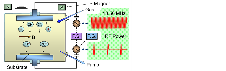
Figure 1. Schematic of the PRF SMP CVD apparatus.
frequency and a duty ratio of 12.5% (defined as the ratio of pulse on-time to total cycle time). The a-CNx:H films were deposited at a gas pressure of 4 Pa. Figure 2 shows the LORF (0 - 800 W) dependence of the on-time deposition rate measured at a UPRF of 100 W. The on-time deposition rate changed a little between 200 and 400 W, being about 27 and 35 nm/min, respectively. During the off-time of LORF, the wafer temperature naturally sank below that of the wafer exposed to continuous discharge plasma [9] [23] .
We measured the optical band gap of a-CNx:H films formed at UPRF/LORF of 100/0 - 800 W, as shown in Figure 3. The optical band gap showed a large decrease from 2.5 to 0.7 eV. This result indicated that the gap was largely dependent on LORF. The refractive index was measured as a function of LORF. At a LORF of 0 - 800 W, the refractive index was almost constant (2.0 - 2.1).

Figure 2. LORF (0 - 800 W) dependence of the on-time deposition rate measured at UPRF of 100 W.

Figure 3. Optical band gap of a-CNx:H films as a function of LORF (0 - 800 W). UPRF was 100 W.
Figure 4 shows the hardness measurements of a-CNx:H films formed at UPRF/LORF of 100/0 - 800 W. There was a large increase in hardness from 15 to 30 GPa in concert with an increase in LORF from 400 to 600 W. The hardness of about 30 GPa was sufficiently higher than that of vitreous silica (SiO2), which was 22 GPa, and a little higher than that of the continuous-discharge plasma CVD films (below 28 GPa) [23] . This high hardness was attributed to periodic ion bombardment over the films and a stable, low substrate temperature.
Figure 5 contains FTIR absorption spectra measured for the a-CNx:H films deposited at UPRF/LORF of 100/0 - 800 W. The thickness of the a-CNx:H film used in the FTIR analysis was controlled to be around 500 nm for all samples, and thickness was almost uniform. The intensities of the absorption bands at 2930 cm−1 (CH3, CH2, and CH bonds) decreased, and those at 1100 - 1700 cm−1 (C=C, C=N, and C=N-H bonds) increased with an increase in LORF [34] . The intensities of the absorption bands at 2190 cm−1 (C≡N bond) and 3300 cm−1 (NH bonds) showed little change with LORF.

Figure 4. Hardness of a-CNx:H films as a function of LORF (0 - 800 W). UPRF was 100 W.

Figure 5. FTIR absorption spectra of a-CNx:H films as a function of LORF (0 - 800 W). UPRF was 100 W. Used gases were i-C4H10 (50 sccm) and N2 (120 sccm).
These a-CNx films of about 20-nm thickness were deposited at 100/800W on the two types of substrates: 100-nm thick Al film deposited on an Si wafer (Al/Si) and 100-nm thick Al film deposited on a glass wafer (Al/glass). Al films were deposited using an Al magnetron sputter with a ring permanent magnet, which we had reported previously [27] . Film characteristics were measured using apparatus with a 50-μm space between the Mo anode (2-mm-diameter) and the sample at a background pressure of about 2 × 10⁻⁵ Pa (Figure 6). Field electron-emission characteristics of a-CNx:H films deposited on Al/Si and Al/glass wafers, are shown in Figure 7(a) and Figure 7(b), respectively. In these and the following figures, a-CNx:H is abbreviated as DLC. A field emission sample was put on the cathode in a vacuum. In this case, an Al film was connected electrically to the cathode using Al-wire. The emission threshold electric field (ETH) was 12 V/μm in each sample, as shown in Figure 7(a) and Figure 7(b). In this experiment, ETH was defined as the applied electric field at the field emission current of 0.01 μA. The FN plot of each a-CNx:H film, shown in the insets of the figures, was nearly linear in both cases.
An SiO2 film of about 50-nm thickness was deposited on the surface of the a-CNx:H/Al/Si sample shown in Figure 7(a). The sample structure is shown in the inset of Figure 8. The SiO2 film was deposited using a SiO2 magnetron sputter with ring

Figure 6. Schematic of field emission measurement apparatus with 50-μm space between anode and sample.

 (a) (b)
Figure 7. (a) Emission current-voltage characteristics of a-CNx:H film deposited at 100/800 W on (a) Al/Si (left), and (b) Al/glass (right) substrates. Insets show layer structures and FN plots.
permanent magnet. Al film was connected electrically to the cathode using Al-wire. Field electron-emission characteristics of SiO2/a-CNx:H/Al/Si are presented in Figure 8. ETH was 14 V/μm. The FN plot of this a-CNx:H film, shown in the inset of the figure, was nearly linear. Electrons were emitted from the a-CNx:H film through the insulating SiO2 film to vacuum. Electron-field emission has usually been discussed using bare amorphous carbon films [35] ; however, this experiment shows that exposuring an a-CNx:H surface to a vacuum is not essential in electron-field emission.
Electrical contact characteristics between Al (100-nm thick) and a-CNx:H (200-nm thick) films was measured using the Al/a-CNx:H/Al device. Figure 9 shows the I-V characteristics of the Al/a-CNx:H/Al structure measured using a semiconductor parameter analyzer (Hewlett Packard 4155A), and the device structure is shown in the inset of the figure. The I-V characteristic reveals that electrical contact between Al and a-CNx:H films is ohmic. The I-V curve indicates that the electrical resistance of this device is 10 Ω. In the other experiment, the contact resistance between this Al/a-CNx:H structure was found to be 5 Ω. In the third experiment, I-V characteristic measurement along the film surface direction found that the resistivity of the film was about 1 × 10⁴ Ω cm.
Electrical insulating and breakdown characteristics of the SiO2 (50-nm thick) film were measured using an Al/SiO2/Al device. Figure 10 shows the I-V characteristic of the Al/SiO2/Al structure, and the device structure is shown in the inset of the figure. The I-V characteristic shows insulating breakdown behavior at about 3.8 V, without demonstrating FN tunneling.
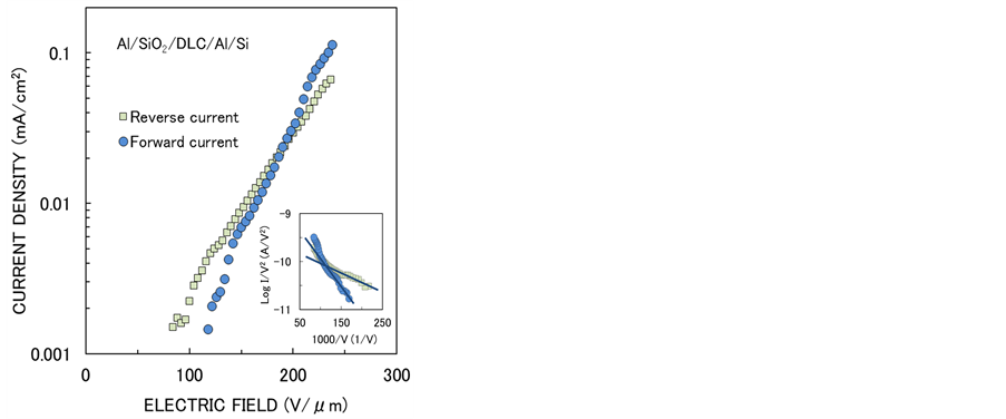
The electron emission characteristic of the a-CNx:H film deposited on an Al/Si substrate was measured using the Al/SiO2/a-CNx:H/Al device. The Al electrode deposited on the SiO2 surface was 4 × 4 mm2 in size. The thickness of SiO2 and a-CNx:H films were 50 and 200 nm, respectively. The I-V characteristic of the Al/SiO2/a-CNx:H/Al structure is shown in Figure 11(a), and the device structure is shown in the inset of the
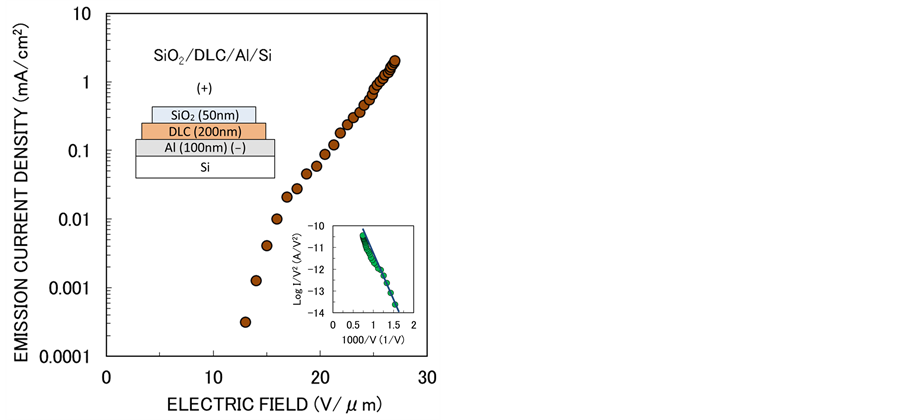
Figure 8. Emission current-voltage characteristics of SiO2/a-CNx:H/Al/Si structure. a-CNx:H film was deposited at 100/800W. Insets show layer structure and FN plot.

Figure 9. I-V characteristic of Al/a-CNx:H/Al structure. Inset shows the layer structure.

Figure 10. I-V characteristic of Al/SiO2/Al structure. Inset shows the layer structure.
figure. The I-V characteristic showed electrical rectifying behavior in both the forward and reverse current directions with a somewhat point-symmetrical shape. Figure 11(b) shows the semi-log plot of the I-V curve shown in Figure 11(a). The FN plot of forward and reverse current directions shown in the Figure 11(b) inset was nearly linear in both current directions. In this experiment, it was difficult to define the standard threshold emission current and ETH.
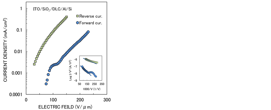
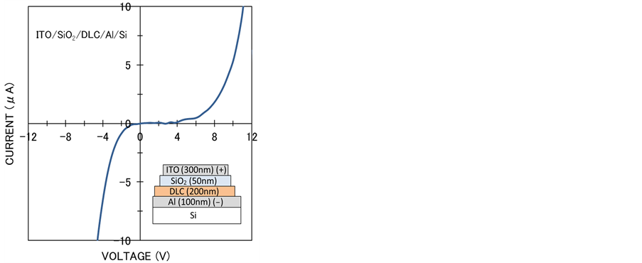
The electron emission characteristic of the a-CNx:H film deposited on the Al/Si substrate was also measured using an indium tin oxide (ITO)/SiO2/a-CNx:H/Al device. The SiO2 and ITO films were deposited using the magnetron sputter with the ring permanent magnet used for the deposition of Al films. The ITO electrode deposited on the SiO2 surface was 4 × 4 mm2 in size. SiO2 and a-CNx:H films were 50 and 200 nm thick, respectively. The I-V characteristic of the ITO/SiO2/a-CNx:H/Al structure is shown in Figure 12(a), and the device structure is shown in the inset of the figure. Here, the I-V characteristic showed electrical rectifying behavior of the forward and reverse current directions with an asymmetrical shape, unlike that of the Al/SiO2/a-CNx:H/Al. Figure 12(b) shows the semi-log plot of the I-V curve shown in Figure 12(a). The FN plot of forward and reverse current directions shown in the inset of Figure 12(b) was nearly linear in both directions. In this experiment, it was difficult to define the standard threshold emission current and ETH.

 (a) (b)
Figure 11. (a) I-V characteristic (left); (b) semi-log plot of I-V curve (right) of Al/SiO2/a-CNx:H/Al structure. Inset shows (a) layer structure, and (b) FN plot.
 (a) (b)
Figure 12. (a) I-V characteristic (left); (b) semi-log plot of I-V curve (right) of ITO/SiO2/a-CNx:H/Al structure. Inset shows (a) layer structure, and (b) FN plot.
In the case of the field electron-emissions shown in Figure 7 and Figure 8, many small craters were created on the surface of samples. Figure 13 shows an example of these craters, which were formed by the vacuum arc discharge at the emission sites, and photographed by laser microscope. The craters always formed instantaneously, before reaching the electric field of ETH (the field emission current of 0.01 μA). On the other hand, no craters were observed in the Al/SiO2/a-CNx:H/Al or ITO/SiO2/a-CNx:H/Al devices (Figure 11 and Figure 12); i.e. no vacuum arc discharges occurred in these structures.
The surface morphology of the a-CNx:H/Al/Si, a-CNx:H/Al/glass, and Al/SiO2/a-CNx:H/ Al/Si used in this experiment was analyzed by AFM; the surfaces are shown in Figures 14(a)-(c), respectively. It was specified that the surfaces of these films were almost flat, and the average peak heights of surface roughness for Figures 14(a)-(c) were about 0.9, 6.3 and 6.0 nm, respectively, over an area of 5 × 5 or 10 × 10 μm2. In Figure 14(c), serious measurement-error noise was observed in the lower half of the image, while there was little error noise observed in the upper half. It was therefore deduced that the typical average peak height of the Al/SiO2/a-CNx:H/Al/Si structure was about 3 nm. From the low average peak heights of the surfaces shown in Figures 14(a)-(c), we could conclude that the observed peaks never caused the concentration of the electric field.
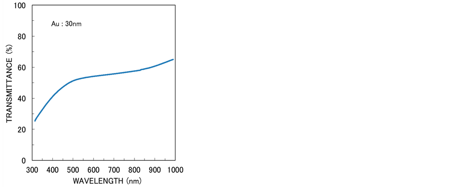
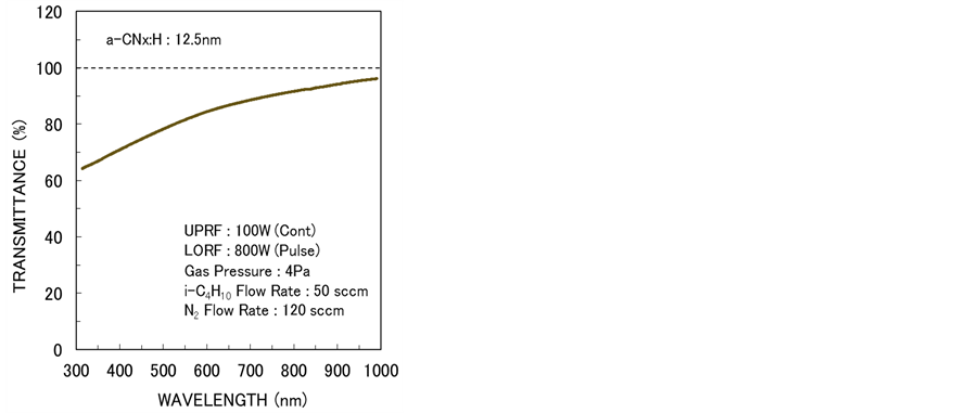
a-CNx:H films about 5 - 300 nm thick were deposited at 100/800W on p-Si substrates (0.01 Ω cm) to form electron transport films (a-CNx:H) for use in PVCs. Figure 15(a) and Figure 15(b) illustrate the film and its structure. Gold ohmic electrodes 30-nm thick, and semitransparent in visible light were deposited for the PVCs (Figure 16(a)) by a magnetron sputter deposition system on the semitransparent a-CNx:H surfaces. The transmittance of those surfaces is shown in Figure 16(b) for 12.5-nm thick a-CNx:H film. The I-V characteristics of a-CNx:H/p-Si PVCs were measured at 25˚C under dark and light conditions. Figure 17(a) and Figure 17(b) show the results for

Figure 13. Photograph of craters formed by the vacuum arc discharge at emission sites.
 (a)
(a)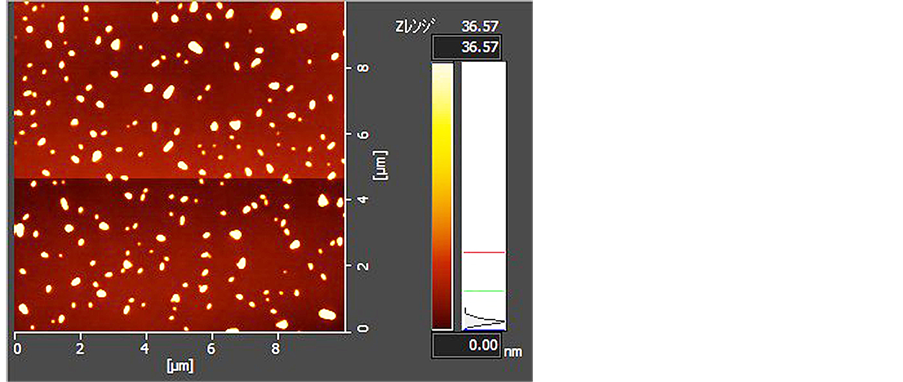 (b)
(b)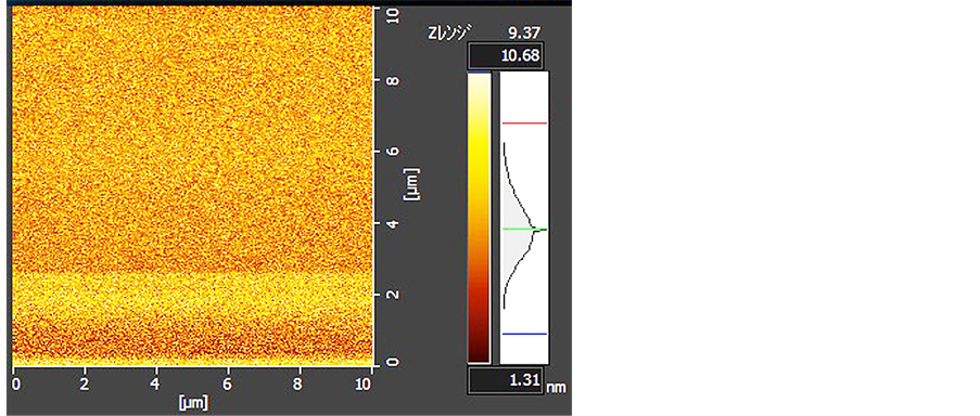 (c)
(c)
Figure 14. Surface morphology of (a) a-CNx:H/Al/Si (upper); (b) a-CNx:H/Al/glass (middle); (c) Al/SiO2/a-CNx:H/Al/Si (lower) measured using AFM. Observation area was 5 × 5 or 10 × 10 μm2.

 (a) (b)
Figure 15. (a) Photograph (left), and (b) structure (right) of fabricated Au/a-CNx:H/p-Si PVC.
 (a) (b)
Figure 16. Transmittances of (a) 30-nm thick Au electrode (left); (b) 12.5-nm thick a-CNx:H (right).

 (a) (b)
Figure 17. I-V characteristics of a-CNx:H/p-Si PVCs measured in dark and light. a-CNx:H thicknesses of (a) 5 (left), and (b) 12.5 (right) nm.
a-CNx:H thicknesses of 5 and 12.5 nm, respectively (Yamashita Denso YSS-80A with AM1.5G, 100 mW/cm2, calibrated by a reference Si photodiode BS-520) [36] [37] . They showed a rectifying curve in the dark, indicating the formation of a heterojunction between the a-CNx:H film and p-Si substrate [9] [10] ; an a-SiCx mixed layer about 2-nm thick would be formed at the heterojunction interface [38] .
In the light, photons emitted from the xenon lamp were barely absorbed by the n-type semitransparent a-CNx:H film, while many photons were absorbed onto the surface layer of the p-Si substrate. The photoconductivity effect was not observed for the thin a-CNx:H film. These absorbed photons generated many electron-hole pairs at the surface layer of the p-Si substrate. The electrons that were excited in conduction bands of p-Si flowed into the a-CNx:H film. The holes excited in valence bands of p-Si drifted to the backside of the p-Si substrate. As our PVC showed a rectifying I-V curve, this a-CNx:H/p-Si heterojunction was thought to resemble to Schottky junction because of the very high electron density of the a-CNx:H films (>1 × 1020 cm−3) [10] . The conversion efficiency of a-CNx:H/p-Si PVCs with a-CNx:H films ~5 - 300 nm thick is shown in Figure 18. A peak conversion efficiency of 0.72% was achieved with an a-CNx:H of 12.5 nm. As a-CNx:H thickness increased from 12.5 to 300 nm, conversion efficiency decreased due to the reduction in light transparency of the a-CNx:H films.
To investigate the generation location of photoelectrons, the external quantum efficiency (EQE) of 25-nm thick a-CNx:H PVC film was measured, as shown in Figure 19. Spectra were measured with an EQE measurement system (Bunkoukeiki CEP-25ML). EQE decreased from 24.3% to 0.07% with an increase of wavelength from 480 to 1100 nm. As the 25-nm thick a-CNx:H film showed no photoconduction, it was clear that electron-hole pairs generated at the thin surface depletion-layer of the p-Si contributed to photoelectron-current generation. As photons with high and low energies are strongly and weakly absorbed, respectively, by the 10-nm thick depletion layer of the

Figure 18. Conversion efficiency of a-CNx:H/p-Si PVCs with a-CNx:H films about 5 - 300 nm-thick.
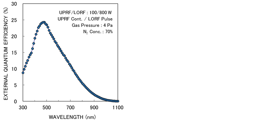
Figure 19. EQE spectra of PVC with 25-nm thick a-CNx:H film.
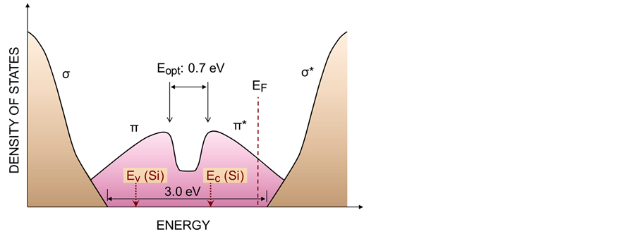
Figure 20. Schematic representation of density of states (DOS) in 100/800W a-CNx:H film.
p-Si [10] (due to the high and low absorption coefficients of Si), EQEs at 480 nm and 1100 nm wavelength became large and small, respectively, as shown in Figure 19.
4. Discussion
Figure 20 is a schematic representation of the density of states (DOS) in the a-CNx:H. The σ bonds of sp3 sites give rise to the σ valence and σ* conduction band states, separated by a wide band gap on the order of 3.0 eV. The π states of sp2 form weaker bonds, which introduce the π valence and π* conduction states within the σ-σ* gap. These states form the band edges and control the optical band gap. The optical band gap (0.7 eV) of the a-CNx:H depends primary on the sp2 fraction [17] [39] .
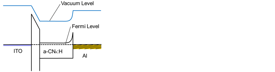
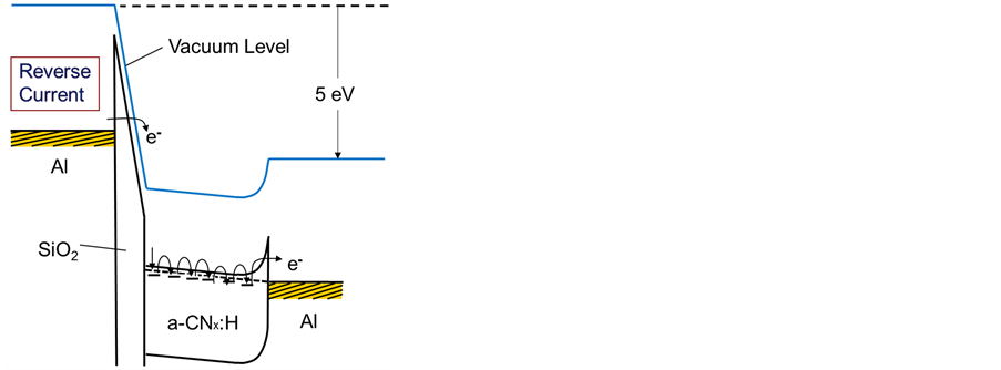
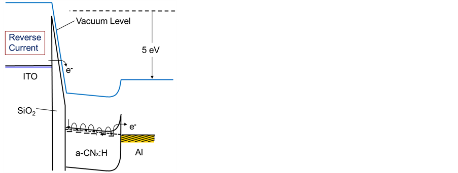
To explain the I-V characteristics shown in Figure 7, Figure 11, Figure 12 and Figure 17, energy band diagrams were proposed and analyzed, as shown in Figures 21(a)-(c). Figure 21(a) shows the proposed flat-band diagram of Al/SiO2/a-CNx:H/Al and the ITO/SiO2/a-CNx:H/Al structure (Figure 11 and Figure 12). The work functions of Al and ITO are 4.1 and 4.7 eV, respectively [40] [41] . The electron affinity of SiO2 is about 1 eV [42] [43] . The valence band edge (a-CNx:H) potential of 5.6 eV was measured using photoemission spectroscopy (Riken Keiki AC-3). Figure 21(a) shows that the electron affinity of this a-CNx:H film is about 2.6 eV. Figure 21(b) and Figure 21(c) show the thermal equilibrium band diagram of Al/SiO2/a-CNx:H/Al and ITO/SiO2/ a-CNx:H/Al structures, respectively.
Figure 22 and Figure 23 show the energy band diagrams in the (a) forward, and (b) reverse current statuses of the I-V curves (Al/SiO2/a-CNx:H/Al and ITO/SiO2/ a-CNx:H/Al) shown in Figure 11 and Figure 12, respectively. Due to the high electron density of a-CNx:H films (>1 × 1020 cm−3), a very thin Schottky barrier is formed at the interface between the a-CNx:H and Al. Between the sp2 clusters located just below the conduction band edge of the σ* states (sp3 sites), which form the Fermi level (EF) in the σ-σ* bands, electrons hopped to nearer CC sp2 clusters by thermal activation beyond the conduction band edge (EC) of σ* states, and conduct slowly by an applied electric field with repeated hopping. In other words, some of smaller sized sp2 clusters with or without N atoms located just below the conduction band edge of the σ* states serve as donors in the σ* conduction band, and create a hopping conduction. Hopping between larger sized sp2 clusters [37] [44] is not adequate in our electron conduction model. Some of the larger sp2 clusters with or without N atoms will be able to absorb photons and form optical band gaps in the sp2 cluster space, i.e., the strongly localized π-π* bands [45] .
 (a)
(a)
 (b) (c)
Figure 21. Proposed energy band diagrams of Al/SiO2/a-CNx:H/Al and ITO/SiO2/a-CNx:H/Al structures. (a) flat-band (upper), thermal equilibrium band diagram of (b) Al/SiO2/a-CNx:H/Al (lower left); (c) ITO/SiO2/a-CNx:H/Al (lower right).

 (a) (b)
Figure 22. Energy band diagrams in (a) forward (left), and (b) reverse (right) current statuses of the I-V curves (Al/SiO2/a-CNx:H/Al).

 (a) (b)
Figure 23. Energy band diagrams in (a) forward (left), and (b) reverse (right) current statuses of the I-V curves (ITO/SiO2/a-CNx:H/Al).
At the interface of a-CNx:H and Al, electrons can be conducted by the tunneling effect. At the interface between SiO2 and a-CNx:H or Al or ITO, electrons can be conducted bidirectionally by FN tunneling. In Figure 22(a) and Figure 22(b), the barrier width is almost the same at the bias voltage of ±5 V, and almost the same current can be conducted. In Figure 23(a) and Figure 23(b), the barrier width is quite different, and the applied electric field in SiO2 is also largely different. As a result, forward and reverse currents becomes low and high, respectively, at a bias voltage of ±5 V because the FN tunneling current depends positively and strongly on the electric field applied in SiO2 space.
Figure 24 is the diagram of the energy band in the electron field emission situation of the a-CNx:H/Al devices in Figure 7(a) and Figure 7(b). The vacuum level on the surface of the a-CNx:H is deformed and lowered by the image potential effect. I do not show an energy band diagram for the case of the SiO2/a-CNx:H/Al sample in Figure 8, because it is almost identical to the case of Al/SiO2/a-CNx:H/Al shown in Figure 22(a).
Figure 25 shows the energy band diagram in the photovoltaic situation of the Au/a-CNx:H/p-Si PVC shown in Figure 17(a) and Figure 17(b). The work function of Au is 4.8 eV [46] . The electron-hole pairs generated at the thin surface depletion-layer of p-Si make possible both electron hopping conductions toward the superficial a-CNx:H layer and hole conductions in the valence band toward the deeper Si wafer. Image potential effects were not considered, and are omitted in the other energy band diagrams shown in Figures 21-23 and Figure 25.
In these experiments, all of the a-CNx:H films (except for the a-CNx:H/p-Si PVC) were deposited on Al films. Al films deposited on Si or glass substrates were connected electrically to the cathode with Al-wire. Si substrates were used to eliminate the influence of the slight surface roughness observed in glass substrates. However, the surface roughness of the glass substrate has never influenced the field emission effect, (i.e., there was a negligible field concentration effect at the surface projections). This experiment shows that Si wafers are not necessary to produce FN tunneling and field emission devices. Al film is a low-cost material compared with Si wafers, and Al/(Si or glass) wafer with no a-CNx:H films coating showed no field emissions. Therefore, Al film is important as a base material for the deposition of a-CNx:H film for the application of
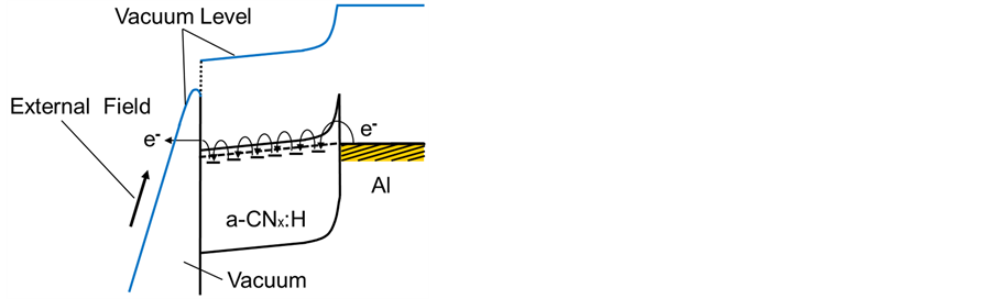
Figure 24. Energy band diagram in electron field emission situation of the a-CNx:H/Al device.
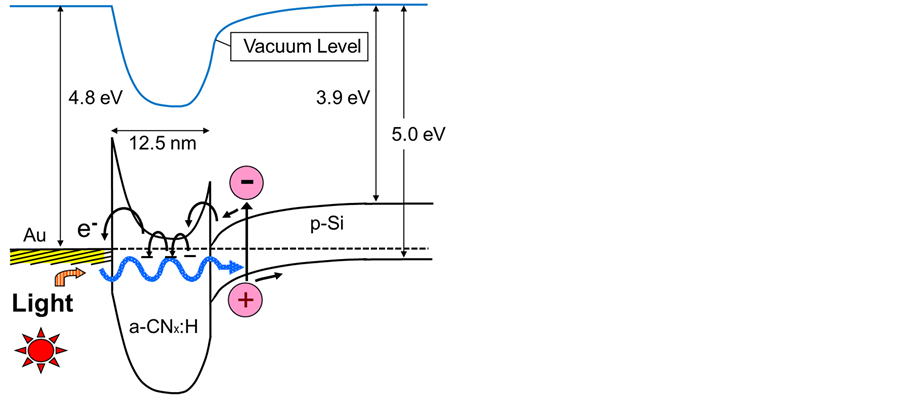
Figure 25. Energy band diagram in photovoltaic situation of a-CNx:H/p-Si PVC.
FN tunneling and field electron-emission devices. This indicates that a-CNx:H film is the key material for easy FN tunneling and field electron-emission.
In this study, I proposed energy band models that are adequate to explain FN electron tunneling, electron field emission, and photovoltaic phenomena. I proposed an electron conduction model formed in an a-CNx:H film using 100/800W PRF SMP CVD, and was able to successfully explain all the FN electron tunneling, electron field emission and photovoltaic phenomena semiquantitatively using the proposed energy band models.
This a-CNx:H film formed by 100/800W PRF SMP CVD would be suitable for application to the electron-conductive electrodes of FN tunneling memory devices, nanoscale vacuum electronics and optical sensors for light, X-ray, and so on.
5. Conclusion
a-CNx:H films were deposited using PRF SMP CVD. Using RF power (lower electrode) modulated by 2.5 kHz pulse frequency, wafers were cooled and high grade a-CNx:H films were formed. At a duty ratio of 12.5% and RF powers of 100/800W, the optical band gap of a-CNx:H film was 0.7 eV. The a-CNx:H films (100/800W) deposited on Al films showed excellent electron emission effects (FN tunneling and field emission), and a-CNx:H/p-Si PVCs were successfully fabricated. All of these electron emission and photovoltaic phenomena were successfully explained semiquantitatively using my proposed electron conduction and energy band model of a-CNx:H. It was found that electrons would hop to nearer (smaller sized) sp2 clusters beyond EC of σ* states, and EF in the σ-σ* bands would be formed just below EC. The electron affinity of this a-CNx:H film would be 2.6 eV. All of our experiments of FN electron tunneling, electron field emission and photovoltaic phenomena could be successfully explained semiquantitatively using my electron conduction model in a-CNx:H.
Acknowledgements
I would like to thank Yoku Murayama, Ken Matsumoto, Hiroki Takeuchi and Takeyuki Kato of Shizuoka University for their support in sample preparation and measurement, and Hideyuki Suzuki and Masanori Kinpara of Hamamatsu Photonics for their support of this experiment.
Cite this paper
Kinoshita, H. (2016) Fowler-Nordheim Tunneling, Photovoltaic Applications and New Band Structure Models of Electroconductive a-CNx:H Films Formed by Supermagnetron Plasma CVD. Journal of Modern Physics, 7, 2008- 2027. http://dx.doi.org/10.4236/jmp.2016.715177
References
- 1. Jung, J.H., Ju, B.K., Kim, H., Oh, M.H., Chung, S.J. and Jang, J. (1998) Journal of Vacuum Science & Technology B, 16, 705-709.
http://dx.doi.org/10.1116/1.589886 - 2. Lin, C.M., Chang, S.J., Yokoyama, M., Chuang, F.Y., Tsai, C.H., Wang, W.C. and Lin, I.N. (1999) Japanese Journal of Applied Physics, 38, 890-893.
http://dx.doi.org/10.1143/JJAP.38.890 - 3. Xu, N.S., Wu, Z.S., Deng, S.Z. and Chen, J. (2001) Journal of Vacuum Science & Technology B, 19, 1370-1372.
http://dx.doi.org/10.1116/1.1387451 - 4. Knapp, W. and Schleussner, D. (2002) Vacuum, 69, 333-338.
http://dx.doi.org/10.1016/S0042-207X(02)00354-8 - 5. Lettington, A.H. (1993) Philosophical Transactions of the Royal Society A, 342, 287-296.
http://dx.doi.org/10.1098/rsta.1993.0022 - 6. Küttel, O.M., Groening, O., Emmenegger, C. and Schlapbach, L. (1998) Applied Physics Letters, 73, 2113-2115.
http://dx.doi.org/10.1063/1.122395 - 7. Semet, V., Binh, V.T., Vincent, P., Guillot, D., Teo, K.B.K., Chhowalla, M., Amaratunga, G.A.J., Milne, W.I., Legagneux, P. and Pribat, D. (2002) Applied Physics Letters, 81, 343-345.
http://dx.doi.org/10.1063/1.1489084 - 8. Kinoshita, H., Ikuta, R. and Murakami, S. (2004) Journal of Vacuum Science & Technology A, 22, 1857-1861.
http://dx.doi.org/10.1116/1.1756878 - 9. Kinoshita, H. and Suzuki, H. (2011) Journal of Modern Physics, 2, 398-403.
http://dx.doi.org/10.4236/jmp.2011.25049 - 10. Kinoshita, H., Ninomiya, Y. and Kato, T. (2013) Japanese Journal of Applied Physics, 52, Article ID: 116201.
http://dx.doi.org/10.7567/JJAP.52.116201 - 11. Amaratunga, G.A. J. and Silva, S.R.P. (1996) Applied Physics Letters, 68, 2529-2531.
http://dx.doi.org/10.1063/1.116173 - 12. Cui, J.B., Robertson, J. and Milne, W.I. (2001) Journal of Applied Physics, 89, 3490-3493.
http://dx.doi.org/10.1063/1.1350626 - 13. Uemura, Y., Murai, S., Koide, Y. and Murakami, M. (2002) Diamond and Related Materials, 11, 1429-1435.
http://dx.doi.org/10.1016/S0925-9635(02)00042-0 - 14. Ilie, A., Ferrari, A.C., Yagi, T., Rodil, S.E., Robertson, J., Barborini, E. and Milani, P. (2001) Journal of Applied Physics, 90, 2024-2032.
http://dx.doi.org/10.1063/1.1381001 - 15. Panwar, O.S., Kumar, S., Rajput, S.S., Sharma, R. and Bhattacharyya, R. (2003) Vacuum, 72, 183-192.
http://dx.doi.org/10.1016/S0042-207X(03)00142-8 - 16. Kinoshita, H. and Otaka, N. (2002) Journal of Vacuum Science & Technology A, 20, 1481-1485.
http://dx.doi.org/10.1116/1.1488946 - 17. Stenzel, O., Vogel, M., Pönitz, S., Petrich, R., Wallendorf, T., Borczyskownski, C.V., Rozploch, F., Krasilnik, Z. and Kalugin, N. (1993) Physica Status Solidi (A), 140, 179-188.
http://dx.doi.org/10.1002/pssa.2211400115 - 18. Wood, P., Wydeven, T. and Tsuji, O. (1995) Thin Solid Films, 258, 151-158.
http://dx.doi.org/10.1016/0040-6090(94)06366-4 - 19. Kinoshita, H. and Murakami, T. (2002) Journal of Vacuum Science & Technology A, 20, 403-407.
http://dx.doi.org/10.1116/1.1446446 - 20. Kinoshita, H., Ikuta, R. and Yamaguchi, T. (2008) Thin Solid Films, 516, 4441-4445.
http://dx.doi.org/10.1016/j.tsf.2007.10.017 - 21. Yamada, H., Tsuji, O. and Wood, P. (1995) Thin Solid Films, 270, 220-225.
http://dx.doi.org/10.1016/0040-6090(95)06892-9 - 22. Kumar, S., Dixit, P.N., Sarangi, D. and Bhattacharyya, R. (1999) Journal of Applied Physics, 85, 3866-3876.
http://dx.doi.org/10.1063/1.369758 - 23. Kinoshita, H. and Yamaguchi, A. (2010) Japanese Journal of Applied Physics, 49, Article ID: 08JF07.
- 24. Kinoshita, H., Yamashita, M. and Yamaguchi, T. (2006) Japanese Journal of Applied Physics, 45, 8401-8405.
http://dx.doi.org/10.1143/JJAP.45.8401 - 25. Kinoshita, H., Kubota, M. and Ohno, G. (2010) Thin Solid Films, 518, 3502-3505.
http://dx.doi.org/10.1016/j.tsf.2009.11.051 - 26. Kinoshita, H. and Yagi, S. (2014) Journal of Physics: Conference Series, 518, Article ID: 012004.
http://dx.doi.org/10.1088/1742-6596/518/1/012004 - 27. Kinoshita, H., Suzuki, S., Taguchi, R. and Takeuchi, H. (2015) Journal of Modern Physics, 6, 1602-1608.
http://dx.doi.org/10.4236/jmp.2015.611162 - 28. Ma, Z.Q. and Liu, B.X. (2001) Solar Energy Materials and Solar Cells, 69, 339-344.
http://dx.doi.org/10.1016/S0927-0248(00)00400-1 - 29. Jones, D.I. and Stewart, A.D. (1982) Philosophical Magazine Part B, 46, 423-434.
http://dx.doi.org/10.1080/01418638208224021 - 30. Kinoshita, H. and Nomoto, K. (1992) Journal of Vacuum Science & Technology A, 10, 1092-1095.
http://dx.doi.org/10.1116/1.578207 - 31. Kinoshita, H., Fukushima, F., Kando, M., Nakagawa, Y. and Tsukada, T. (2000) Journal of Applied Physics, 88, 2263-2267.
http://dx.doi.org/10.1063/1.1288700 - 32. Kinoshita, H. and Otaka, N. (2004) Vacuum, 74, 99-104.
http://dx.doi.org/10.1016/j.vacuum.2003.12.071 - 33. Tauc, J. (1974) Amorphous, Liquid Semiconductors. Plenum Press, New York, 159-220.
http://dx.doi.org/10.1007/978-1-4615-8705-7 - 34. Mutsukura, N. (2001) Diamond and Related Materials, 10, 1152-1155.
http://dx.doi.org/10.1016/S0925-9635(00)00595-1 - 35. Robertson, J. (1999) Journal of Vacuum Science & Technology B, 17, 659-665.
http://dx.doi.org/10.1116/1.590613 - 36. Kinoshita, T., Dy, J.T., Uchida, S., Kubo, T. and Segawa, H. (2013) Nature Photonics, 7, 535-539.
http://dx.doi.org/10.1038/nphoton.2013.136 - 37. Kinoshita, T., Nonomura, K., Jeon, N.J., Giordano, F., Abate, A., Uchida, S., Kubo, T., Seok, S.I., Nazeeruddin, M.K., Hagfeldt, A., Grätzel, M. and Segawa, H. (2015) Nature Communications, 6, Article Number: 8834.
http://dx.doi.org/10.1038/ncomms9834 - 38. Schäfer, J., Ristein, J., Miyazaki, S. and Ley, L. (1997) Journal of Vacuum Science & Technology A, 15, 408-414.
http://dx.doi.org/10.1116/1.580499 - 39. Carey, J.D., Forrest, R.D., Poa, C.H. and Silva, S.R.P. (2003) Journal of Vacuum Science & Technology B, 21, 1633-1639.
http://dx.doi.org/10.1116/1.1593642 - 40. Chen, C., Liao, C., Wei, L., Zhong, H., He, R., Liu, Q., Liu, X., Lai, Y., Song, C., Jin, T. and Zhang, Y. (2016) Scientific Reports, 6, Article Number: 22203.
- 41. Nüesch, F., Rotzinger, F., Si-Ahmed, L. and Zuppiroli, L. (1998) Chemical Physics Letters, 288, 861-867.
http://dx.doi.org/10.1016/S0009-2614(98)00350-9 - 42. Ballarotto, V.W., Breban, M., Siegrist, K., Phaneuf, R.J. and Williams, E.D. (2002) Journal of Vacuum Science & Technology B, 20, 2514-2518.
http://dx.doi.org/10.1116/1.1525007 - 43. Cook Jr., T.E., Fulton, C.C., Mecouch, W.J., Tracy, K.M., Davis, R.F., Hurt, E.H., Lucovsky, G. and Nemanich, R.J. (2003) Journal of Applied Physics, 93, 3995-4004.
http://dx.doi.org/10.1063/1.1559424 - 44. Katsuno, T., Godet, C., Loir, A.S. and Garrélie, F. (2006) Journal of Non-Crystalline Solids, 352, 1421-1424.
http://dx.doi.org/10.1016/j.jnoncrysol.2005.09.038 - 45. Sakurai, K., Kinoshita, H., Ohno, G., Nakanishi, Y. and Kubota, M. (2008) Japanese Journal of Applied Physics, 47, 7216-7219.
http://dx.doi.org/10.1143/JJAP.47.7216 - 46. Anderson, P.A. (1959) Physical Review, 115, 553-554.
http://dx.doi.org/10.1103/PhysRev.115.553