Wireless Engineering and Technology
Vol.3 No.3(2012), Article ID:21465,4 pages DOI:10.4236/wet.2012.33019
FPGA Design and Implementation of a Convolutional Encoder and a Viterbi Decoder Based on 802.11a for OFDM
![]()
Department of Communication Engineering, Hefei University of Technology, Hefei, China.
Email: sunyan2058@sina.com, zzding@mail.ustc.edu.cn
Received March 5th, 2012; revised April 1st, 2012; accepted April 9th, 2012
Keywords: FPGA; Convolutional Encoder; Viterbi Decoder; IEEE 802.11a; OFDM
ABSTRACT
In this paper, a modified FPGA scheme for the convolutional encoder and Viterbi decoder based on the IEEE 802.11a standards of WLAN is presented in OFDM baseband processing systems. The proposed design supports a generic, robust and configurable Viterbi decoder with constraint length of 7, code rate of 1/2 and decoding depth of 36 symbols. The Viterbi decoder uses full-parallel structure to improve computational speed for the add-compare-select (ACS) modules, adopts optimal data storage mechanism to avoid overflow and employs three distributed RAM blocks to complete cyclic trace-back. It includes the core parts, for example, the state path measure computation, the preservation and transfer of the survivor path and trace-back decoding, etc. Compared to the general Viterbi decoder, this design can effectively decrease the 10% of chip logic elements, reduce 5% of power consumption, and increase the encoder and decoder working performance in the hardware implementation. Lastly, relevant simulation results using Verilog HDL language are verified based on a Xinlinx Virtex-II FPGA by ISE 7.1i. It is shown that the Viterbi decoder is capable of decoding (2, 1, 7) convolutional codes accurately with a throughput of 80 Mbps.
1. Introduction
The wireless local area network (WLAN) is considered as one of the most effective wideband access ways between electronic devices. The IEEE 802.11a standard [1] for WLAN is based on Orthogonal Frequency Division Multiplexing (OFDM), supporting multiple transmission modes, providing data rate up to 54 Mbps in the 5 GHz band. In order to overcome frequency selective weaknesses from distortion channels in the above-mentioned OFDM-WLAN systems, strong Forward Error Correction (FEC) technologies which have been widely utilized in digital communication applications especially such as the Viterbi Algorithm (VA) are employed. The VA was first introduced as an available scheme for decoding convolutional codes in 1967 [2]. Later, the convolutional codes and VA laid a significant influence in combating with the channel distortion effects such as multipath fading and intersymbol interference. Shaking changes have been made on FPGA technologies over the recent years. Complex real-time signal processing tasks can yet be fulfilled owing to high clock speeds and huge gate densities provided by FPGA. Many efficient structures of Viterbi decoder are researched to decrease the survivor path memory since it can dominate the chip area. Some designs can reduce the memory size significantly [3]. But they cannot be commercialized because of wiring area. Most commercial products [4] still use the classical two-pointer trace-back scheme [5] and demand memory of size 4*K*N bits (K is the constraint length, N is the number of states). An alternative scheme using dual-port memory is proposed recently [6]. The memory requirement is halved while the number of trace-back multiplexers (N to 1) increase one to three.
Convolutional codes are a kind of non-block codes whose performances are superior to block codes in the same coding efficiency situation [7]. Their coding scheme makes information elements have correlations by means of exclusive-or operation, resulting in the increase of transmission redundancy. Based on these correlations, the VA can be used for decoding and error correction in the receiving end. The complexity of software and hardware implementation for VA are growing exponentially with the increase of the m (m is the number of shift registers); Therefore, careful design has to be made to realize such a practical decoder. With the FPGA technology development the VA operation problem has been solved to a great extent. This makes the Viterbi the most extensive, robust and capable decoding algorithm when the value of m is less than or equal to 10. Without a doubt, the primary purpose of any decoder design might be to decrease the FPGA area, reduces the power consumption and improve the decoding performance. The Virtex-II family is a platform FPGA developed for high performance from low-density to high-density designs which are optimized for high speed with low power consumption. The device XC2V2000 of this family can excellently meet the performance and stability requirements of the encoder and decoder according to the experiments. The designs are described using Verilog HDL for the hardware implementation on the above FPGA and it can be configurable.
The remainders of this paper are organized as follows. In Section 2, The analysis and FPGA design of (2, 1, 7) convolutional encoder are presented. Section 3 shows the algorithm and the Viterbi decoder architecture. In Section 4, the implementation results analyses are provided based on a Xinlinx virtex2 FPGA by ISE 7.1i. The paper is concluded in Section 5.
2. Convolutional Encoder Analysis and Design
Convolutional Encoder Analysis and Architecture
Convolution codes are better codes of error controlling performance. Convolutional encoder outputs are not only associated with the encode elements at present, but also affected by several ones before. (n, k, m) is used for describing convolutional codes, where k are the input encode elements, n are the output encode elements and m are the shift register numbers of convolution encoder. Usually, the value of n and k is smaller and k is less than n, but the number of shift registers takes larger value.
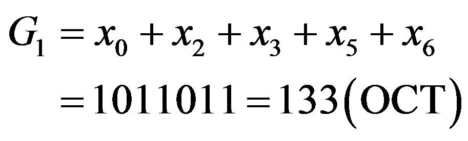
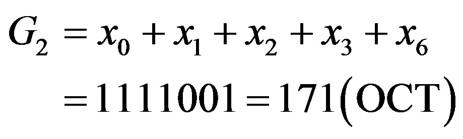
In WLAN standards the convolutional codes are defined by given generator polynomials with constraint length of 7 and code rate of 1/2, resulting in 64 trellis states. The given generator polynomials codes are G1 = 133(OCT) and G2 = 171(OCT), equally
 (1)
(1)
 (2)
(2)
Figure 1 indicates the block diagram of (2, 1, 7) convolutional encoder. The (2, 1, 7) convolutional encoder consists of six shift registers and two exclusive-or gates. When starting coding, all these registers are reset for initialization. Every shift register is equivalent to a flip flop. These six flip flops are connected in series to complete shifting and updating operation under the action of the clock pulse. The exclusive-or gates are used for modular-2 adders to obtain the coding data. With every clock pulse the encoder outputs two bits according to the generator polynomials whenever one binary bit is inputted. The output is not only relevant with the current input binary bit, but also influenced by the inputs six clock pulses before.
3. The Viterbi Decoder
3.1. Viterbi Algorithm
Viterbi is known as a maximum likelihood decoding algorithm of convolutional codes for estimating and searching the most likely survivor path in the trellis according to the receiving sequences, meanwhile the error during transmission can be corrected. This algorithm is based on calculating the hamming distance for each branch and the path that is most likely through the trellis will maximize that metric [8]. For binary encoders, the corresponding trellis is composed of L + 1 sections with  nodes each, where L is the length of the message to be decoded in bits and K is the constraint length of the code. While the entire trellis must be considered for optimal sequence detection, practical realizations will work only on a section of the complete trellis with Ltb
  stages, where is called trace-back length [9].
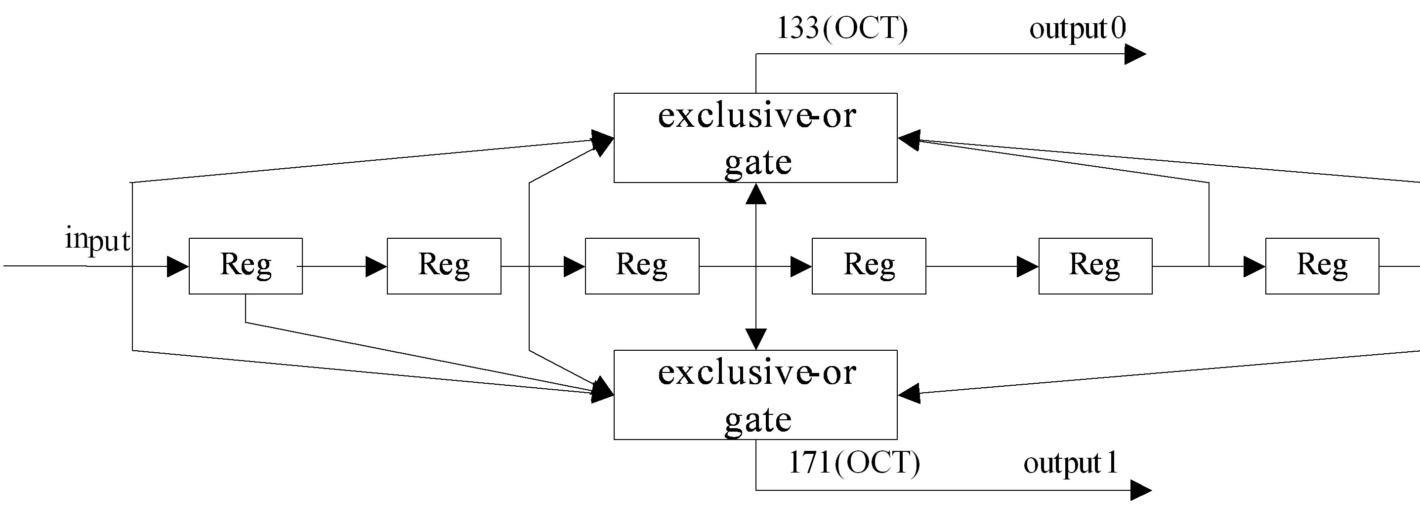
Figure 1. (2, 1, 7) convolutional encoder for OFDM-WLAN.
3.2. The Architecture of the Viterbi Decoder
In this paper, hamming distance computation module, ACS module, survivor path storage and management module, trace-back module, timing controller module and minimum value choice module are included for the Viterbi decoder.
However, there are two remarkable problems before the design. One is the choice of decoding depth; the other is the survivor path storage. In general, the VA starts to trace-back until the survivor path is to zero, and then finds a best path. But this would not only increase decoding delay, and will cause the problem of much bigger storage capacity. Despite the growing decoding depth can improve the decoding accuracy, according to former experiences the system performance has no significant influence when decoding depth is five times as much to 10 times of the registration numbers [9]. Based on the 802.11a decoding depth is set to thirty six. Convolutional decoder has sixty four states, it needs to store the sixty four survivor paths and keep the corresponding path lengths. Therefore, the capacity of each RAM block should be set to sixty four storage units, the size of each storage unit equals to decoding depth.
The whole hardware architecture is shown in Figure 2. The proposed Viterbi decoder works as follows:
Step 1, two parallel binary bits are inputted into the Viterbi decoder with every clock pulse, and then the hamming distance computation module begins to work when the input enabling signal is valid. It calculates sixty four groups of hamming distance. Each group consists of two because each current state can be reached by two possible paths.
Step 2, the ACS modules begin to work. Cumulative hamming distance one clock before is added to hamming distance of the new branch path correspondingly. After adding operation each current state gets two new cumulative hamming distances, and then the ACS module compares the size of the two cumulative distances and selects the smaller one as a survivor. The path of the survivor represents survived path. The smaller cumulative hamming distance becomes the benchmark for the next computation. Survivor paths of all the sixty four states are stored in RAM blocks.
Step 3, sixty four survivor paths are stored in the RAM blocks and each of them equals to decoding depth when the decoding depth is reached, then sixty four cumulative hamming distances are inputted into the minimum value choice module. This module outputs the minimum value to trace-back module, then the trace-back module reads survivor values from the paths storage RAM blocks according to survivor path values. The outputs of the backtracking module are the Viterbi decoding results.
3.2.1. The Hamming Distance Computation Module
This module compares the received codes with the expected codes of the current state and calculates the hamming distance between them. The hamming distance computation schematic diagram is shown in Figure 3.
Table 1 gives the algorithm expressions for the hamming distance calculation of two received codes under the four possible values of the excepted codes, where data_in1 and data_in2 stand for the two-bit inputs in the trellis.
3.2.2. ACS Module
This module is the core part of the Viterbi decoder to
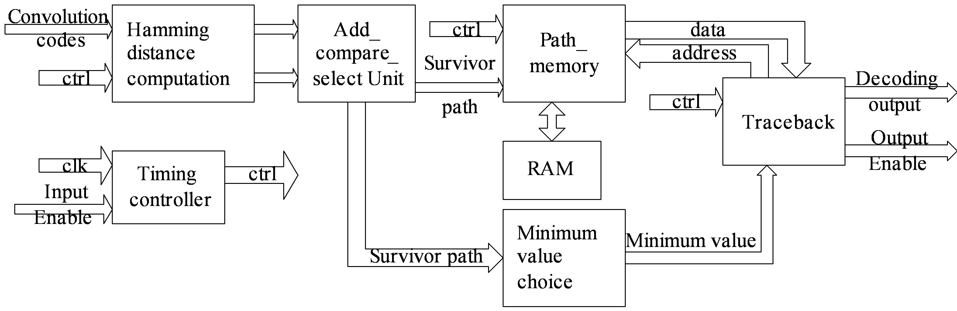
Figure 2. The hardware architecture of Viterbi decoder.
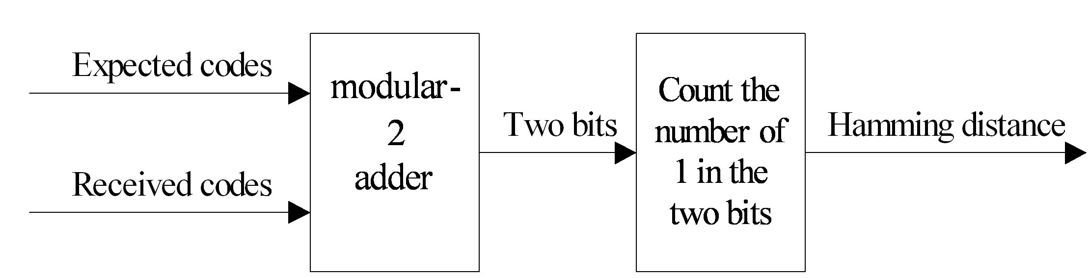
Figure 3. Hamming distance computation schematic diagram.

Table 1. Hamming distance calculation.
complete addition, comparison and selecting function. There are sixty four states in the decoder; each state uses an ACS module. So the decoder needs sixty four ACS modules. Parallel processing is used for this module. This design cannot only improve the computational speed, but also reduce the system delay. The most important is relatively simple hardware implementation. In addition, a counter with thirty six counting cycles is designed to start the ACS module and measure time. With more and more input bits, cumulative hamming distance is also on the rise. This brings trouble to memory storage. In order to prevent overflow, cumulative hamming distance is moved two bits wide rightwards. Before decoding, in order to guarantee the all-zero state is the first choice, the cumulative hamming distance of all-zero state is initialized to zero, while the rest take higher values. Eight is set in other states. The hardware architecture of the ACS module is shown in Figure 4" target="_self"> Figure 4.
3.2.3. Survivor Path Storage and Management Module
This module is used for storing and managing survivor path values of the ACS modules. Three RAM blocks work by turns. The following is a detailed description.
Step 1, the first RAM block is written to survivor paths for sixty six clock periods which equals to decoding depth, and then it begins to trace-back and decode.
Step 2, the second RAM block begins to be written to survivor paths like the first one. After another decoding depth the second one begins to trace-back and the third one begins to be written to survivor paths.
Step 3, when the third RAM block is full, it begins to trace-back. At this time the first RAM block is free, therefore, the survivor paths can be written to it again.
In this study, decoding and trace-back is performed at the same time. Three RAM blocks are used for this module because the write operation and read operation are not the same start and end. When the decoding depth is reached in the first RAM block, sixty four cumulative hamming distances of all the states are inputted to the minimum value choice module; this module needs thirty three clock periods to finish the work. In this period the second one is being written. The first RAM block just starts decoding when the second one is full. If the first one that should be written is not free when the write operation of the second one is over, the third RAM block should be provided for the new write operation. Therefore, two RAM blocks cannot be used by turns. The working process of RAM blocks is showed in Figure 5.
3.2.4. Minimum Value Choice Module
This module compares the size of sixty four cumulative
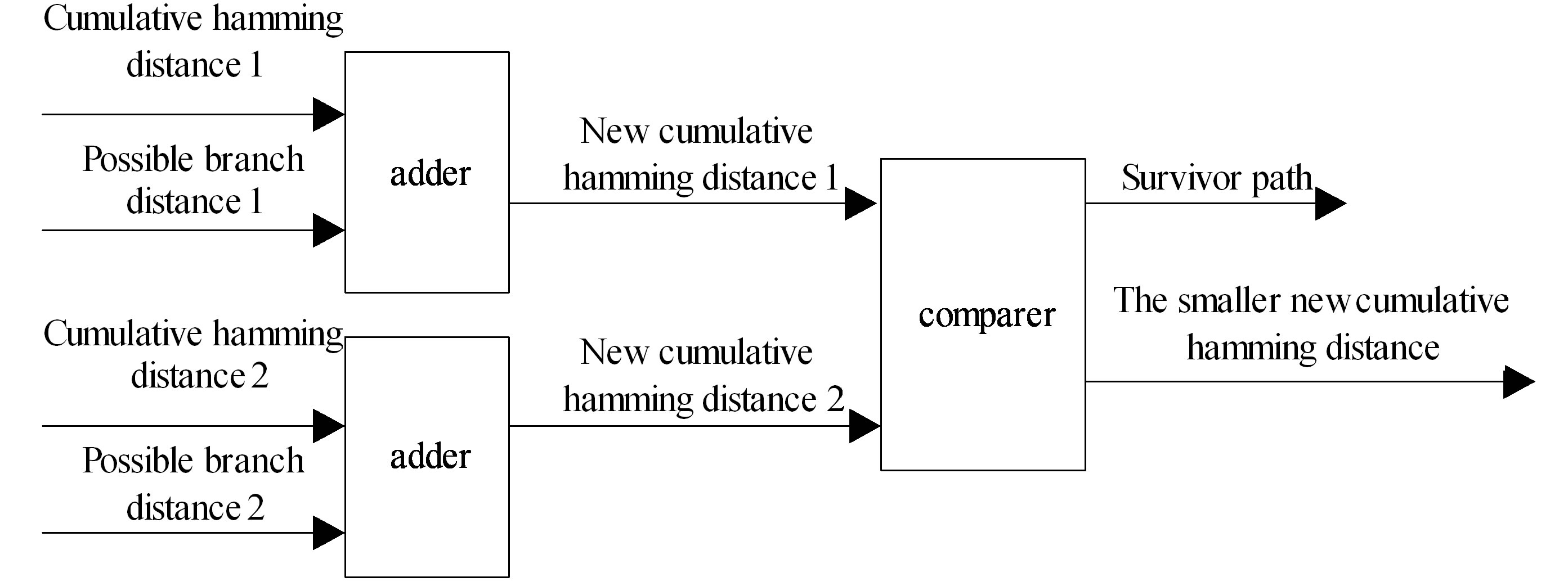
Figure 4. The hardware architecture of the ACS module.

Figure 5. The working process of RAM blocks.
hamming distances when the decoding depth is reached. Its aim is to obtain the minimum value and the initial state of trace-back. The working time of the minimum value choice module cannot be greater than the decoding depth; otherwise the decoding errors will occur. This module consists of two same comparison units; the first comparison unit compares the size of the former thirty two cumulative hamming distances, the second one compares the size of the remaining thirty two cumulative hamming distances. Finally the result of the first comparison unit is compared with the second one, and then the minimum value is achieved. The whole process needs thirty three clock cycles, which is less than the decode depth.
However, the delay with thirty three clock cycles is made due to using two parallel comparators. More comparators can be designed for reducing delay, while the more resources and area will be occupied. The design should be carefully weighed between the delay and resource consumption.
3.2.5. Trace-Back Module
There are two algorithms of survivor paths storage and management for decoding. One is register-exchange algorithm; the other is trace-back. The principles and hardware implementation of the register-exchange algorithm [10,11] are more easily. Compared with trace-back, this algorithm has one obvious advantage that is the smaller output delay. But it brings two mortal flaws, one is lots of power consumption when the memory contents of each state are always read and written for updating survivor paths with every clock pulse, the other is too complex internal connection relationships to restrict the FPGA design. So it is rarely used in practical applications. Trace-back is a classic algorithm and widely used, and uses memories to store survivor paths of each state. The former trace-back point is determined by the best initial state and the corresponding survivor paths every clock. The trace-back is completed after thirty six clock periods. The hardware structure of the algorithm is simple to manage and control for FPGA.
As shown in Figure 6, from the K moment to K + 1 moment, there are two optional paths to reach the state 000000 and they originate from the state 000000 and 000001. There is a difference between the lowest orders of the two states; the lowest order stands for the input bit of the Viterbi encoder five clock pulses before, the rest bits represent others from different moments. The top digit of the state 000000 is the survivor value at the K + 1 moment. It indicates the input bit in the K + 1 moment, in other words, also the decoded value. All these survivor values constitute the only survivor path. A counter with thirty six count cycles is designed for recording the trace-back time to determine the trace-back end. Survivor

Figure 6. Trace-back schematic diagram.
paths are extracted for updating the next trace-back point according to the current one. The Viterbi decoder begins to output when the counter counts to the decoding depth. In addition, the decoding sequences of trace-back are opposite to the practical ones, so adjustments should be made during outputting.
4. Implementation Results Analysis
4.1. Simulation Scenarios
The Xilinx ISE is a comprehensive and powerful FPGA design environment. The ISE 7.1i simulation tools are used for the logic synthesis aims to map the design to the FPGA target technology. Xilinx Virtex-II, XC2V2000, with speed grade –4 and Verilog HDL code has been selected to realize this scheme. The test-bench file is written to provide the clock frequency, related timing settings, control signals and code sequences for both the encoder and the decoder. One hundred and eight random binary bits which equal to total memory capacity are given to the (2, 1, 7) convolutional encoder. In order to validate the error correction performance of the Viterbi decoder, one error is placed deliberately every ten bits in the simulation results of convolutional encoder, then the convolutional codes after appending errors are considered as the Viterbi encoder inputs for verification. The bit error rate is much higher than the actual system to reflect the design superiority.
4.2. Results Analysis
The simulation results of (2, 1, 7) convolutional encoder for OFDM-WLAN are shown in Figure 7. During decoding, first, ACS modules works for thirty six clock periods, second, minimum value choice module works for thirty three clock periods to obtain the initial state of trace-back, third, the trace-back module begins to work for thirty six clock periods. Finally, decoding results begin to be outputted next clock pulse after sequence adjustments. From the above, we can draw the conclusion that the Viterbi decoder outputs are delayed for one hundred and six clock periods. Figure 8 makes clear that the decoder can correct all the errors and meet timing requirements.
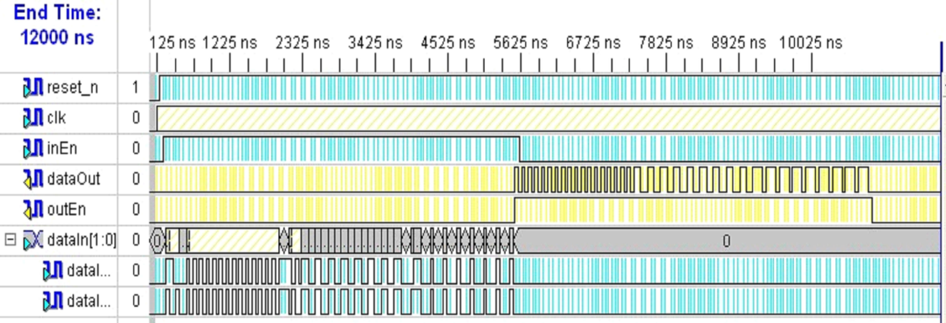
Figure 7. Simulation waveforms of convolutional decoder for OFDM-WLAN, 10-bit erros are corrected.

Figure 8. Simulation waveforms of convolutional decoder for OFDM-WLAN, 10-bit errors are corrected.
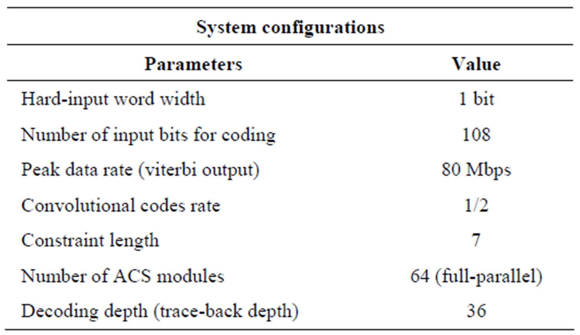
Table 2. System configurations.
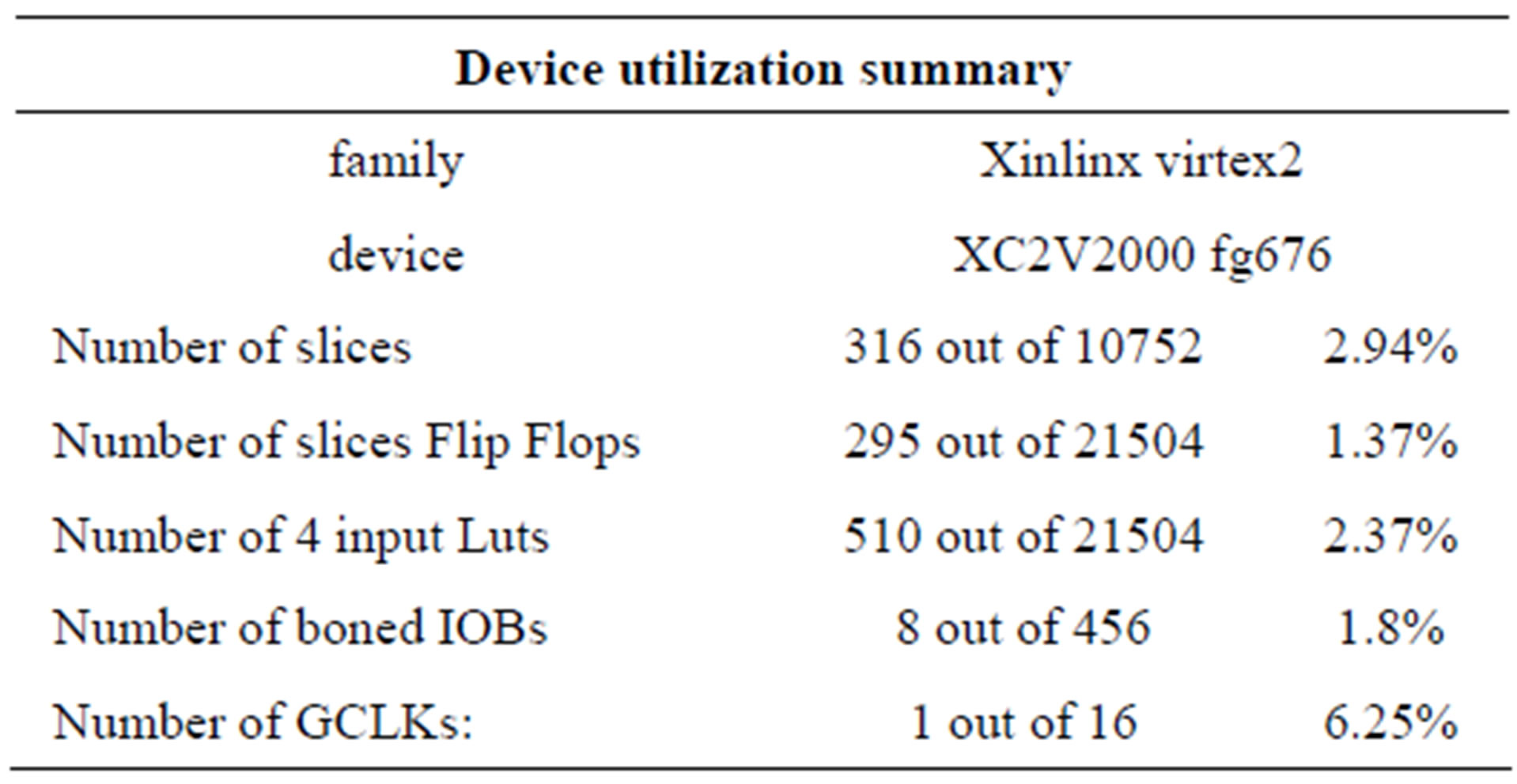
Table 3. Device utilization summary.
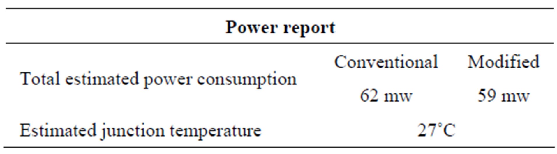
Table 4. The power consumption reports.
Otherwise, Tables 2 and 3 show the system configurations and device utilization, the power consumption reports are given in Table 4.
In addition, there are some disorders in the decoding process if the input bits are not integer times of decoding depth. But decoding depth can be modified to solve this problem; therefore, the decoding depth should be set according to the actual situation.
5. Conclusion
In this paper, a (2, 1, 7) convolutional encoder is proposed for FPGA design and implementation, and then an adaptive, low-power, parallel Viterbi decoder with a constraint length of 7 and a code rate of 1/2 is presented. The designs are functionally verified in Xinlinx ISE 7.1 environments. The synthesis results show that the FPGA implementation can run with frequency up to 80 MHz. Compared to the solutions with generic decoder, the proposed scheme uses significantly less logic resources on the FPGA. The design takes about 2.94% of the total chip logic elements. The maximum operating frequency is 80 MHz that is found adequate to our applications.
REFERENCES
- IEEE Std. 802.11, “Wireless LAN Medium Access Control (MAC) and Physical Layer (PHY) Specifications: High Speed Physical Layer in the 5 GHz band,” 1999.
- A. J. Viterbi, “Error Bounds for Convolutional Coding and an Asymptotically Optimum Decoding Algorithm,” IEEE Transactions on Information Theory, Vol. IT-13, No. 2, 1967, pp. 260-269. doi:10.1109/TIT.1967.1054010
- P. J. black and T. H. Meng, “Hybrid Survivor Path Architectures for Viterbi Decoders,” IEEE ICASSP92, Vol. 1, 1993, pp. 433-436.
- L. Christopher, et al., “A Fully Integrated Digital Demodulation and forward Error Correction IC for Digital Satellite Television,” IEEE Custom Integrated Circuits Conference, Santa Clara, 1-4 May 1995, pp. 281-284.
- G. Feygin, “Architectural Tradeoffs for Survivor Sequence Memory Management in Viterbi Decoder,” IEEE Transactions on Communications, Vol. 41, 1993 pp. 426- 428.
- D. A. Luthi, A. Mogre, N. Ben-Efraim and A. Gupta, “A Single-Chip Concatenated FEC Decoder,” IEEE Custom Integrated Circuits Conference, IEEE Custom Integrated Circuits Conference, Santa Clara, 1-4 May 1995.
- R. E. Blahut, “Theory and Practice of Error Control Codes,” Addison-Wesley, New York, 1983.
- A. J. Viterbi, “Convolutional Codes and Their Performance Incommunication Systems,” IEEE Transactions on Communications, Vol. COM-19, No. 5, 1971, pp. 751- 772. doi:10.1109/TCOM.1971.1090700
- S. Haene, A. Burg, D. Perels, P. Luethi, N. Felber and W. Fichtner, “FPGA Implementation of Viterbi Decoders for MIMO-BICM,” IEEE Radio and Wireless Conference, Atlanta, 19-22 September 2004, pp. 734-738.
- D. A. El-Dib and M. I. Elmasry, “Modified RegisterExchange Viterbi Decoder for Low-Power Wireless Communications,” IEEE Transactions on Circuits and Systems I, Vol. 51, 2004, pp. 371-378. doi:10.1109/TCSI.2003.822396
- G. Feygin and P. Gulak, “Architectural Tradeoffs for Survivor Sequence Memory Management in Viterbi Decoders,” IEEE Transactions on Communications, Vol. 41, 1993, pp. 425-429. doi:10.1109/26.221067