World Journal of Condensed Matter Physics
Vol.2 No.3(2012), Article ID:22131,6 pages DOI:10.4236/wjcmp.2012.23022
Ab Initio Calculations for the Effect of Pressure on the Structural Properties of Si Nanoclusters
![]()
1Physics Department, College of Science, University of Babylon, Babylon, Iraq; 2Basic Science Department, College of Veterinary Medicine, University of Babylon, Babylon, Iraq.
Email: *abdullettif@yahoo.com
Received April 14th, 2012; revised May 20th, 2012; accepted May 30th, 2012
Keywords: Nanocrystals; Pressure; Structural; Si
ABSTRACT
Lattice constant, bulk modulus, Young modulus, valence band width, conduction band width, energy gap, vibrational energy, and plasmon energy have been calculated under compression and tensile stresses in the range (0 ± 10 GPa) for 8, 54, 128 atom clusters of silicon by means of density functional theory method with restricted Hartree-Fock theory within the framework of large unit cell approach. It is found that the results deduced from eight atom cluster are in good agreement with the corresponding experimental values. On the other hand, bulk modulus, young modulus, valence band width, energy gap, and Plasmon energy increase (decrease) under compression (tensile), while volume decreases (increases) with compression (tensile). The vibrational energy has a minimum value at the ground state point. The conduction band width has no systematic behavior with pressure.
1. Introduction
Electronics is one of many interesting fields that IV materials can be implied in [1-6] so they have been subjected to extensive investigations [7-14]. Silicon, a very important semiconductor, is the principal component of most semiconductor devices; it is widely used in the semiconductors industry because it remains a semiconductor at higher temperatures than the semiconductor germanium, and because its native oxide forms a better semiconductor/dielectric interface than any other materials. The applications of silicon are in the electronic current conduction control (transistors), IC, detectors, solar cells and so forth. Nanocrystalline silicon (nc-Si) has small grains of crystalline silicon within the amorphous phase (a-Si). One of the most important advantages of nanocrystalline silicon is that it has increased stability over (a-Si) [15-20].
Understanding the properties of Si nanocrystals is an interesting field. Up to our knowledge, the effect of pressure on the properties of Si nanocrystals has not been comprehensively investigated. So the aim of the present work is to achieve this task.
Density functional theory (DFT) method in addition to Hartree-Fock (HF) theory within the Large unit cell (LUC) method [14] are used for calculating the total energy, lattice constant, bulk modulus (B), Young modulus (Y), valence band width (VBW), conduction band width (CBW), energy gap (Eg), vibrational energy (Fvib), and plasmon energy (Epl).
2. Method
The self-consistent Hartree-Fock method is used in the present work to obtain the electronic structure of silicon nanocrystals. Correlation corrections can be neglected in some closed-shell calculations (which is the case of the present work) using Koopmans theorem [21] owing to the cancellation of correlation corrections with relaxation. STO-3G basis states are used as the simplest basis to reach higher number of atoms [20,22-24].
Large unit cell (LUC) method coupled with ab initio Hartree-Fock self-consistent electronic structure calculations are used in the present work. LUC method was formulated and used previously to investigate the electronic of several kinds of bulk materials including diamond [20,23-25]. Semiempirical LUC calculations were performed previously for silicon nanocrystals [22] with smaller number of atoms. This method uses (k = 0) approximation, that is one point in the wave vector space. The LUC method is one kind of supercell methods with the above k = 0 restriction. In this method, and instead of adding more k points, the single central cell is expanded to contain more atoms, which are called core atoms in the present work. We found this method very suitable for describing the core of a nanocrystal since it still has the outer dangling bonds that are saturated by surface atoms. The method does not expand to contain the whole space; instead it contains only the real number of atoms in a nanocrystals core that has nearly the exact diamond structure [14]. Gaussian 03 program has been used for the present calculations [26].
3. Calculations
After the structure optimization, we calculate the lattice constant (ao), the cohesive energy (Ec) and total energy (Eo) in the ground state (zero temperature and 1 atmosphere). The cohesive energy is calculated from (Equation (17) in Ref. [27]). Results were fitted to Equation (1), the equation of state of Murnaghan, to estimate the change of energy with pressure E(V), [28] and to determine the change of vibrational energy Fvib Equation (2) [29],
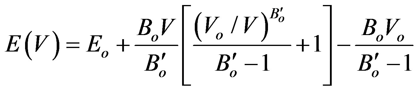 (1)
(1)
 (2)
(2)
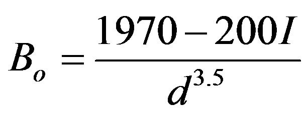
where PT is the isothermal pressure, Vo and Bo are the volume and the bulk modulus of the unit cell at the standard conditions and V is the volume at any pressure. The bulk modulus is calculated by Cohen empirical formula [30]:
 (3)
(3)
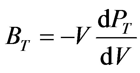
I is the ionicity factor which equals 0, 1 and 2 for IV, III-V and II-V groups respectively [30], d is the interatomic distance [31]. Then the isothermal bulk modulus at any pressure (BT) has been calculated as [32]:
 (4)
(4)
where (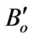 ) is the derivative of bulk modulus at zero pressure. The volume is calculated from:
 (5)
(5)
The results of pressure vs. volume  relation are shown in Figure 1. On the other hand, the Young modulus is calculated from [33],
 (6)
(6)
where ε is the strain. We have from Mijbil et al. [34] that the energy of plasmon (Epl) is:
 (7)
(7)

Figure 1. The variation of volume with pressure.
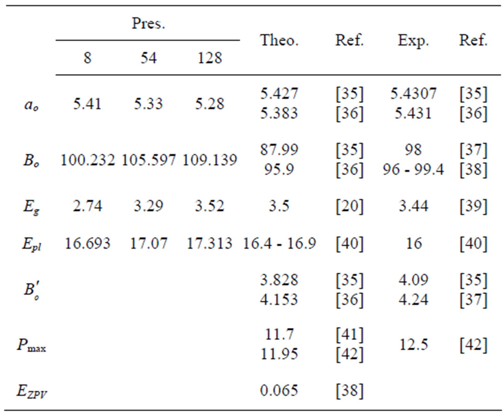
Table 1. The structural properties of Si at (0 K and 1 atm), the dimensions are Å, GPa, eV for length, pressure, and energy respectively.
where .
.
4. Results and Discussion
Our calculated structural properties at (0 K & 1 atm) compared with other results are shown in Table 1.
It is known that DFT underestimates the band gap [43] due to the discontinuity of the potential of exchangecorrelation [44] which explains the difference between our results and the experimental data.
The compression stress increases the density and decreases volume due to the shrinkage of orbitals [45] as shown in Figure 1, and the distance between atoms [46], which entails an increment in the bond strength [47] and bulk modulus [48] (Figure 2) because the bulk modulus depends upon the density directly, and the young modulus which depends upon the bulk modulus [49], and vice verse for the tensile stress.
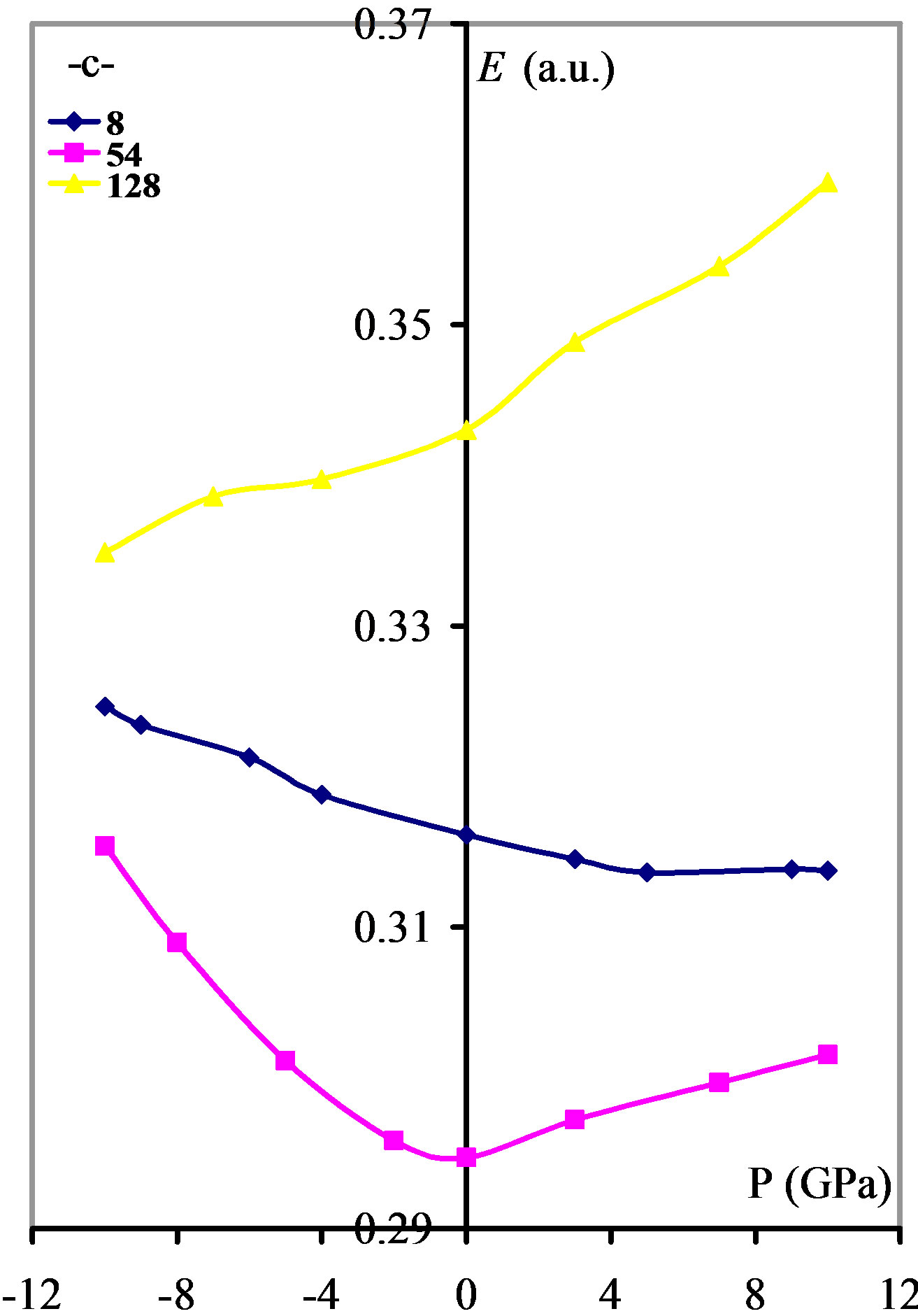
Figure 3 shows an increment in the plasmon energy with compression and a reduction of it with tensile stress. Kornyushin has showed that the plasma affects the charge distribution and so the sound wave [50]. On the other hand, the phonon frequency affects the effective charge [51], which depends upon the charge distribution and determines the plasma frequency [52]. Compression stress, according to Sanjurjo, increases the effective charge for IV-IV materials and vice verse [51]. Meanwhile, the effective charge reduction, according to Burstein, decreases the plasmon frequency [52], and then one can find that our results are in good agreement with experiment [51] for the behavior of plasmon energy. The vibrational energy increases with both stresses.
In order to get a further comprehension, the vibrational energy is considered. Its behavior is the same for all clusters and takes a minimum value at the standard conditions (0 K, 1 atm). It is known that atoms vibration is determined by phonons [53], and the velocity of sound depends on the atoms arrangement [54], while crystal is considered as a group of harmonic oscillators [55], according to Born-von Kármán theory. From all above and according to Polit who mentioned that the change of the lattice constant changes the charge distribution which affects the atoms’ force field and these potentials modify the vibration energy [56]. On the other hand at zero temperature and according to Equation (2), the vibrational energy depends upon the behavior of the total energy which increases with stresses due to repulsion and attraction forces [57].
Energy gaps and valence band widths increase with compression, as shown in Figures 4(a) and (b) and they decrease with tensile stress, whereas the conduction band has no systematic behavior with pressure as shown in Figure 4(c). It should be pointed out that increasing compressing means increasing overlapping and Coulomb interaction.
5. Conclusion
From the results of the present work, it shown that the density functional theory method with the restricted Hartree-Fock theory within the framework of large unit constitutes a powerful approach for investigating the structural properties of semiconductor nanoclusters. It is found that the bulk modulus, Young modulus, valence band width, energy gap, and plasmon energy increase with compression, whereas the conduction band width has no systematic behavior with pressure. The conduction band

Figure 2. The variation of bulk modulus with pressure.

Figure 3. The variation of plasmon energy with pressure.
 (a)
(a) (b)
(b) (c)
(c)
Figure 4. The effect of pressure on the: (a) Energy gap; (b) Valence band width; and (c) Conduction band width.
behavior needs more investigation, and it could be attributed to the different coulomb interactions and the delocalization of the p orbitals.
REFERENCES
- M. Gabrysch, “Electronic Properties of Diamond,” Uppsala University, 2008. http://urn.kb.se/resolve?urn=urn:nbn:se:uu:diva-8675
- M. Virgilio, G. Pizzi and G. Grosso, “Optical Gain in Short Period Si/Ge Superlattices on [001]-SiGe Substrates,” Journal of Applied Physics, Vol. 110, No. 8, 2011, Article ID: 083105. doi:10.1063/1.3651196
- M. Upadhyay, S. Murugavel, M. Anbarasu and T. R. Ravindran, “Structural Study on Amorphous and Crystalline State of Phase Change Material,” Journal of Applied Physics, Vol. 110, No. 8, 2011, Article ID: 083711. doi:10.1063/1.3653265
- F. Cataldo, “Carbon Allotropy and Carbon Black,” Kautschuk Gummi Kunststoffe, Vol. 54, No. 1-2, 2001, pp. 22-28.
- C. W. Myles, J. Dong and O. F. Sankey, “Structural and Electronic Properties of Tin Clathrate Materials,” Physical Review B, Vol. 64, 2001, Article ID: 165202. doi:10.1103/PhysRevB.64.165202
- M. Gaith and I. Alhayek, “Correlation between Overall Elastic Stiffness, Bulk Modulus and Interatomic Distance in Anisotropic Materials: Semiconductors,” Reviews on Advanced Materials Science, Vol. 21, No. 2, 2009, pp. 183-191.
- R. E. Stallcup II, L. M. Villarreal, S. C. Lim, I. Akwani, A. F. Aviles and J. M. Perez, “Atomic Structure of the Diamond (100) Surface Studied Using Scanning Tunneling Microscopy,” Journal of Vacuum Science and Technology B, Vol. 14, No. 2, 1996, pp. 929-932. doi:10.1116/1.589177
- B. K. Serdega, E. V. Nikitenko and Prikhodenko, “Effect of Surface Condition on Strain in Semiconductor Crystal Sample,” Semiconductor Physics, Quantum Electronics and Optoelectronics, Vol. 4, No. 1, 2001, pp. 9-11.
- J. Pollmann, P. Krüger, M. Rohlfing, M. Sabisch and D. Vogel, “Ab Initio Calculations of Structural and Electronic Properties of Prototype Surfaces of Group IV, III-V and II-VI Semiconductors,” Applied Surface Science, Vol. 104-105, 1996, pp. 1-16. doi:10.1016/S0169-4332(96)00114-6
- A. Otero-de-la-Roza and V. Luaña, “Topological Characterization of the Electron Density Laplacian in Crystals. The Case of the Group IV Elements,” Journal of Chemical Theory and Computation, Vol. 6, No. 12, 2010, pp. 3761-3979. doi:10.1021/ct100269e
- L. A. Woldering, L. Abelmann and M. C. Elwenspoek, “Predicted Photonic Band Gaps in Diamond-Lattice Crystals Built from Silicon Truncated Tetrahedrons,” Journal of Applied Physics, Vol. 110, No. 4, 2011, Article ID: 043107. doi:10.1063/1.3624604
- Q. Zhou, X. Hu, K. Al-Hemyari, K. McCarthy, L. Domash and J. A. Hudgings, “High Spatial Resolution Characterization of Silicon Solar Cells Using Thermoreflectance Imaging,” Journal of Applied Physics, Vol. 110, No. 5, 2011, Article ID: 053108. doi:10.1063/1.3629979
- J. Kim and D. Ahn, “Effect of Indirect Interband Absorption in Ge/SiGe Quantum Wells,” Journal of Applied Physics, Vol. 110, No. 8, 2011, Article ID: 083119. doi:10.1063/1.3656688
- N. A. Nama, M. A. Abdulsattar and A. M. Abdul-Lettif, “Surface and Core Electronic Structure of Oxidized Silicon Nanocrystals,” Journal of Nanomaterials, Vol. 2010, 2010, Article ID: 952172. doi:10.1155/2010/952172
- S. M. Sze and K. K. Ng, “Physics of Semiconductor Devices,” 3rd edition, John Wiley & Sons, New York, 2007.
- S. J. Clark and G. J. Ackland, “Vibrational and Elastic Effects of Point Defects in Silicon,” Physical Review B, Vol. 48, No. 15, 1993, pp. 10899-10908. doi:10.1103/PhysRevB.48.10899
- M. Luppi and S. Ossicini, “Ab initio Study on Oxidized Silicon Clusters and Silicon Nanocrystals Embedded in SiO: Beyond the Quantum Confinement Effect,” Physical Review B, Vol. 71, No. 3, 2005, Article ID: 035340.
- T. Van Buuren, L. N. Dinh, L. L. Chase, W. J. Siekhaus and L. J. Terminello, “Changes in the Electronic Properties of Si Nanocrystals as a Function of Particle Size,” Physical Review Letters, Vol. 80, No. 17, 1998, pp. 3803- 3806. doi:10.1103/PhysRevLett.80.3803
- P. Carrier, “Curvature Effects on Optical Response of Si Nanocrystals in SiO2 Having Interface Silicon Suboxides,” Physical Review B, Vol. 80, No. 7, 2009, Article ID: 075319. doi:10.1103/PhysRevB.80.075319
- M. A. Abdulsattar and K. H. Al-Bayati, “Corrections and Parametrization of Semiempirical Large Unit Cell Method for Covalent Semiconductors,” Physical Review B, Vol. 75, No. 24, 2007, Article ID: 245201. doi:10.1103/PhysRevB.75.245201
- W. Hehre, L. Radom, P. Schileyer and J. Pople, “Ab Initio Molecular Orbital Theory,” Wiley, New York, 1986.
- M. A. Abdulsattar, “Size Effects of Semiempirical Large Unit Cell Method in Comparison with Nanoclusters Properties of Diamond-Structured Covalent Semiconductors,” Physica E, Vol. 41, No. 9, 2009, pp. 1679-1688. doi:10.1016/j.physe.2009.06.003
- A. Harker and F. Larkins, “A Large Unit Cell Semiempirical Molecular Orbital Approach to the Properties of Solids. I. General Theory,” Journal of Physics C, Vol. 12, 1979, pp. 2487-2495.
- A. Harker and F. Larkins, “A Large Unit Cell Semiempirical Molecular Orbital Approach to the Properties of Solids. II. Covalent Materials: Diamond and Silicon,” Journal of Physics C, Vol. 12, 1979, pp. 2497-2508.
- R. Evarestov, M. Petrashen and E. Lodovskaya, “The Translational Symmetry in the Molecular Models of Solids,” Physica Status Solidi (b), Vol. 68, No. 1, 1975, pp. 453-461. doi:10.1002/pssb.2220680145
- M. J. Frisch, G. W. Trucks, H. B. Schlegel, et al., “Gaussian 03,” Revision B.01, Gaussian, Inc., Pittsburgh, 2003.
- I. O. Radi, M. A. Abdulsattar and A. M. Abdul-Lettif, “Semiempirical LUC-INDO Calculations on the Effect of Pressure on the Electronic Structure of Diamond,” Physica Status Solidi (b), Vol. 244, No. 4, 2007, pp. 1304- 1317. doi:10.1002/pssb.200541329
- C. A. Perottoni, A. S. Pereira and J. A. H. da Jornada, “Periodic Hartree-Fock Linear Combination of Crystalline Orbitals Calculation of the Structure, Equation of State and Elastic Properties of Titanium Diboride,” Journal of Physics: Condensed Matter, Vol. 12, No. 32, 2000, pp. 7205-7222. doi:10.1088/0953-8984/12/32/305
- J. Xie, S. P. Chen, J. S. Tse, S. de Gironcoli and S. Baroni, “High-Pressure Thermal Expansion, Bulk Modulus, and Phonon Structure of Diamond,” Physical Review B, Vol. 60, No. 13, 1999, pp. 9444-9449. doi:10.1103/PhysRevB.60.9444
- J. Zheng, C. H. A. Haun, A. T. S. Wee, R. Wang and Y. Zheng, “Ground State Properties of Cubic C-BN Solid Solutions,” Journal of Physics: Condensed Matter, Vol. 11, No. 3, 1999, pp. 927-935. doi:10.1088/0953-8984/11/3/030
- S. Q. Wang and H. Q. Ye, “Plane-Wave Pseudopotential Study on Mechanical and Electronic Properties for IV and III-V Crystalline Phases with Zinc-Blende Structure,” Physical Review B, Vol. 66, 2002, Article ID: 235111. doi:10.1103/PhysRevB.66.235111
- T. Faisst, “Temperature Dependence of the Thermal Expansion Coefficient, Bulk Modulus and Magnetic Grueneisen Constant of Nickel near the Curie Point,” Journal De Physique, Vol. 49, No. 12, 1988, pp. 65-66. doi:10.1051/jphyscol:1988819
- W. Kim, M. Kim, Y. Chang, J. Shin and J. Bae, “Fatigue Crack Growth Behavior of NR and HNBR Based Vulcanizates with Potential Application to Track Pad for Heavy Weight Vehicles,” Macromolecular Research, Vol. 11, No. 2, 2003, pp. 73-79. doi:10.1007/BF03218333
- Z. Y. Mijbil, H. I. Aboud and A. M. Abdul-Lettif, “Variation of the Structural Properties of IV Element Nano Clusters Due to Tensile Stress,” World Journal of Condensed Matter Physics, Vol. 2, 2012, pp. 16-23. doi:10.4236/wjcmp.2012.21003
- P. E. Van Camp, V. E. Van Doren and J. T. Devreese, “Ground-State and Electronic Properties of Covalent Solids,” Physical Review, Vol. 38, No. 17, 1988, pp. 12675- 12678. doi:10.1103/PhysRevB.38.12675
- S. Q. Wang and H. Q. Ye, “Plane-Wave Pseudopotential Study on Mechanical and Electronic Properties for IV and III-V Crystalline Phases with Zinc-Blende Structure,” Physical Review B, Vol. 66, 2002, Article ID: 235111. doi:10.1103/PhysRevB.66.235111
- P. K. Lam, M. L. Cohen, and G. Martinez, “Analytic Relation between Bulk Moduli and Lattice Constants,” Physical Review B, Vol. 35, No. 17, 1987, pp. 9190-9194. doi:10.1103/PhysRevB.35.9190
- S. H. Lee, J. H. Kang and M. H. Kang, “Structural Properties of Semiconductors in the Generalized Gradient Approximation,” Journal of the Korean Physical Society, Vol. 31, No. 3, 1997, pp. 811-814.
- M. Welkowsky and R. Braunstein, “Interband Transitions and Exciton Effects in Semiconductors,” Physical Review B, Vol. 5, No. 3, 1972, pp. 497-509. dio:10.1103/PhysRevB.5.497
- C. Kittel, “Introduction to Solid State Physics,” 5th edition, John Wiley & Sons, New York, 1976.
- A. Mujica, A. Rubio, A. Munoz and R. J. Need, “High Pressure Phaces of Group-IV, III-V, and II-VI Compounds,” Reviews of Modern Physics, Vol. 75, 2003, pp. 863-907. doi:10.1103/RevModPhys.75.863
- J. R. Chelikowsky, "High-Pressure Phase Transition in Diamond and Zinc-Blende Semiconductors,” Physical Review B, Vol. 35, No. 3, 1987, pp. 1174-1180. doi:10.1103/PhysRevB.35.1174
- S. Casolo, E. Flage-Larsen, O. M. Løvvik, G. R. Darling and G. F. Tantardini, “Role of the Self-Interaction Error in Studying First Principles Chemisorption on Graphene,” 2010. http://arxiv.org/abs/1002.4117v2
- M. Kuisma, J. Ojanen, J. Enkovaara and T. T. Rantala, “Kohn-Sham Potential with Discontinuity for Band Gap Materials,” 2010. http://arxiv.org/abs/1003.0296v3
- J. P. Connerade, P. Kengkan, P. A. Lakshmi and R. Semaoune, “Scaling Laws for Atomic Compressibility,” Journal of Physics B: Atomic and Molecular Optical Physics, Vol. 33, 2000, pp. L847-L854.
- S. M. Sze, “Semiconductor Devices: Physics and Technology,” Dar Al-Hikma, Mosul, 1990.
- J. Z. Jiang, H. Lindelov, L. Gerward, K. Ståhl, J. M. Recio, P. Mori-Sanchez, S. Carlson, M. Mezouar, E. Dooryhee, A. Fitch and D. J. Frost, “Compressibility and Thermal Expansion of Cubic Silicon Nitride,’’ Physical Review B, Vol. 65, 2002, Article ID: 161202(R). doi:10.1103/PhysRevB.65.161202
- M. P. D’Evelyn and T. Taniguchi, “Elastic Properties of Translucent Polycrystalline Cubic Boron Nitride as Characterized by the Dynamic Resonance Method,” GE Research & Development Center, General Electric Company, 1998.
- B. T. Wang, P. Zhang, H. L. Shi, B. Sun and W. D. Li, “Mechanical and Chemical Bonding Properties of Ground State BeH2,” The European Physical Journal B, Vol. 74, No. 3, 2010, pp. 303-308. doi:10.1140/epjb/e2010-00081-x
- L. C. M. Miranda and D. ter Haar, “Plasma Effects in Sound Amplification in Piezo-Electric Semiconductors,” Revista Brasileira de Física, Vol. 2, No. 2, 1972, pp. 77- 86.
- J. A. Sanjurjo, E. López-Cruz, P. Vogl and M. Cardona, “Dependence on Volume of the Phonon Frequencies and the IR Effective Charges of Several III-V Semiconductors,” Physical Review B, Vol. 28, No. 8, 1983, pp. 4579- 4584. doi:10.1103/PhysRevB.28.4579
- E. Burstein, S. Perkowitz and M. H. Brodsk, “The Dielectric Properties of the Cubic iv-vi Compound Semiconductors,’’ Journal De Physique, Vol. 29, No. 11-12, 1968, pp. 78-83. doi:10.1051/jphyscol:1968411
- K. Parliński, “First-Principles Calculations of Vibrational and Thermodynamical Properties of Solids,” Materials Science-Poland, Vol. 23, No. 2, 2005, pp. 357-363.
- T. Iitaka and T. Ebisuzaki, “First-Principles Calculation of Elastic Properties of Solid Argon at High Pressures,” Riken Review, No. 48, 2001, pp. 12-15.
- J. Xie, S. de Gironcoli, S. Baroni and M. Scheffler, “First-Principles Calculation of the Thermal Properties of Silver,” Physical Review B, Vol. 59, No. 2, 1999, pp. 965-969. doi:10.1103/PhysRevB.59.965
- J. Polit, E. M. Sheregii, J. Cebulski, B. V. Robouch, A. Marcelli, M. Cestelli Guidi, M. Piccinini, A. Kisiel, P. Zajdel, E. Burattini and A. Mycielski, “Phonon and Vibrational Spectra of Hydrogenated CdTe,” Journal of Applied Physics, Vol. 100, 2006, Article ID: 013521. doi:10.1063/1.2211368
- J. N. Murrel, S. F. A. Kettle and J. M. Tedder, “The Chemical Bond,” 2nd Edition, University of Basrah, Basrah, 1982.
NOTES
*Corresponding author.