Soft Nanoscience Letters
Vol.3 No.1(2013), Article ID:26573,8 pages DOI:10.4236/snl.2013.31004
Nitrification of Reactively Magnetron Sputter Deposited Ti-Cu Nano-Composite Thin Films
![]()
Department of Physics, Faculty of Science, Valieasr University of Rafsanjan, Rafsanjan, Iran.
Email: a.rahmati@vru.ac.ir, alirahmati1980@gmail.com
Received September 27th, 2012; revised November 28th, 2012; accepted December 17th, 2012
Keywords: Nano-Composite; Reactive Magnetron Sputtering; Ti Inserted Cu3N; Interstitial N Excess
ABSTRACT
A metalloid Ti13Cu87 target was sputtered by reactive DC magnetron sputtering at various substrate temperatures in an Ar-N2 mixture ambient. The sputtered species were condensed on Si (111), glass slide and Potsssium bromide (KBr) substrates. The as-deposited films were characterized by X-ray diffraction (XRD), Fourier transform infrared (FTIR) spectroscopy, Scanning electron microscope (SEM), energy dispersive X-ray spectroscopy (EDX), optical spectrophotometry and four point probe technique. The as-deposited films present composite structure of nano-crystallite cubic anti-ReO3 structure of Ti inserted Cu3N (Ti:Cu3N) and nano-crystallite face centre cubic (fcc) structure of Cu. The titanium atoms and sequential nitrogen excess form a solid solution within the Cu3N crystal structure and accommodate in crystal lattice and vacant interstitial site, respectively. Depending on substrate temperature, unreacted N atoms interdiffuse between crystallites and their (and grain) boundaries. The films have agglomerated structure with atomic Ti:Cu ratio less than that of the original targets. A theoretical model has been developed, based on sputtering yield, to predict the atomic Ti:Cu ratio for the as-deposited films. Film thickness, refractive index and extinction coefficient are extracted from the measured transmittance spectra. The films’ resistivity is strongly depending on its microstructural features and substrate temperature.
1. Introduction
Various researches demonstrated the possibility of obtaining a large variety of non-equilibrium microstructure and phase compositions in thin films produced by DC magnetron sputtering. Particularly, several studies were focused on the production of metal alloys made of partly miscible or immiscible elements, deposited in chemically inert (Ar) or in reactive (e.g. Ar-N2) atmosphere. The potential interest in magnetron sputter process rely on the possibility of producing thin films with new properties, markedly different from those of corresponding equilibrium bulk phases when one considers a nano-composite that can be formed, e.g. by combining nano-crystalline phases or by embedding nano-crystalline domains in an amorphous matrix. It is now demonstrated that co-deposition of elements (from different targets or from a mixed target) whose phase diagram presents a wide miscibility gap is a prerequisite for forming non-equilibrium nanocrystalline or amorphous phases. This tendency to form non-crystalline phase is further increased by sputter deposition in a reactive atmosphere [1-9].
Copper nitride has been attracted much attentions due to its low decomposition temperature and sequential applications as write-once optical recording media [10-12], as micrometric conductive lines [13], as an insulating barrier in magnetic tunnel junctions [14]. Although, copper nitride has been widely studied, but little information is available in the literature concerning Cu3N based composite thin films. In this study, a titanium copper bicomponent target was reactively sputtered at Ar-N2 ambient at various substrate temperatures. The aims of this communication are to investigate micro-structural, morphological, chemical, some electrical and optical properties of reactive DC magnetron sputter deposited and nitrided Ti-Cu films.
2. Experimental Methods
A sintered Ti-Cu target (13 at.%Ti, 76 mm in diameter and 4.5 mm thickness) was reactively sputtered at Ar-N2 gas mixture, and the sputtered species were deposited on ultrasonically pre-cleaned Si (111), glass slide and KBr substrates. The deposition conditions were listed in Table 1.
The films structure was studied by X-ray diffraction (XRD) in  scan mode with CuK
  radiation (1.5418Å). The crystallites size was estimated from the full width at half maximum (FWHM) of strongest XRD peak using Scherrer formula. The chemical bonding was characterized by Fourier transform infrared (FTIR) spectroscopy (FTIR spectrometer Bruker Tensor 27). Films morphology and their chemical composition were determined using scanning electron microscope and energy dispersive X-ray spectrometer (SEM/EDX, Philips XL 30). Also, an estimation of the atomic ratio was made in according to sputtering yield. Optical studies were performed by measuring transmittance in the wavelength region 360 - 1100 nm using spectrophotometer (Shimadzu, UV-1700 Pharma Spec) at room temperature. These measurements allowed obtaining refractive index, extincttion coefficient and meaning film thickness. The electrical resistivity of the films at room temperature was deduced from measurement using four point probe method.
3. Results and Discussion
3.1. Structural Properties and Chemical Bonding
Figure 1 shows the effect of substrate temperature on Xray diffraction (XRD) pattern of nitrided Ti-Cu thin films deposited on Si (111) substrate. The films are amorphous at lower substrate temperature (i.e. 45˚C), but at higher substrate temperature (70˚C, 110˚C, 150˚C and 180˚C), they are composed of nano-crystallite cubic anti ReO3 structure of Ti inserted Cu3N (Ti:Cu3N) and nano-crystallite fcc structure of Cu.
Copper nitride has a cubic anti-ReO3 type structure and exhibits a vacant site at the centre of the cell [15]. Ti atoms cannot exclusively be positioned at the centre of a stoichiometric Cu3N cell. The lattice constant has been estimated from the position of the (100) diffraction peak of Cu3N structure. Table 2 indicates the lattice constant of Ti inserted Cu3N (Ti:Cu3N) at various substrate temperatures. Indeed, the value of the lattice constant of Ti:Cu3N crystallites (except for samples prepared at sub strate temperature of 150˚C) is still lower than the calculated value of Cu3MN (M = Cu, Zn, Pd, Ag) [16]. Since titanium atom exhibits a higher radius than M = Cu, Zn, Pd and Ag ones, substitution of the vacant site by titanium atoms in a Cu3N cell centered by titanium may not be further considered. Here, the formation of copper vacancies in Cu3N cell substituted by Ti atoms was considered to explain the measured lattice constant. Lattice constant for sample prepared at substrate temperature of 150˚C has lower value than stoichiometric Ti-free Cu3N (i.e. 0.3815 nm [17]). In most works, the stoichiometry of Cu3N thin films has been deduced from XRD data (having a change in the lattice parameter) [17-23].
The evolution of the film lattice constant is due to the variation in nitrogen stoichiometry [24-26]. However, there is no information about the position of excess nitrogen in the Cu3N unit cell [24]. Due to sensitivity of
Table 1. The deposition conditions.
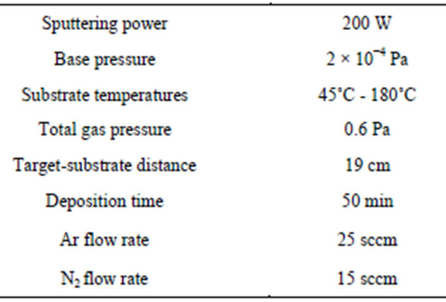
Table 2. Deposition conditions, deposition rate, lattice constant and mean crystallite size of Ti:Cu3N, atomic Ti:Cu ratio and resistivity of the nitrided Ti-Cu films at different substrate temperature.
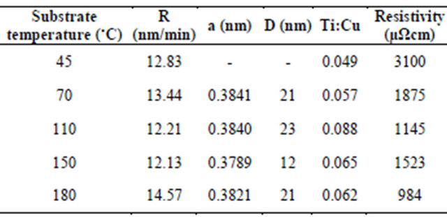
chemical composition to characterization method, lattice constant of Cu3N revealed good qualitative criterion for composition determination. The samples prepared at substrate temperature of 70˚C, 110˚C, 180˚C are N rich or over-stoichiometric, but the sample prepared at substrate temperature of 150˚C is N poor or substoichiometric. Addition of titanium to Cu3N films does not change the cubic anti ReO3 structure of Cu3N (Figure 1). Within the deposition conditions tested in this study (except the samples prepared at substrate temperature of 150˚C), the both of Ti:Cu3N and Cu phases are detected by XRD. No metallic titanium or titanium nitride diffraction lines are exhibited. Figure 2 depicts FTIR spectra of nitrided TiCu films deposited on KBr substrate at various substrate temperature, the infrared absorption of which has been deduced. Typical absorption bands occurred around 667 and 1037 cm−1 are attributed to Cu-N and Ti-N stretch vibrations, respectively [13,27,28]. The Ti-N bond formation shows, titanium addition accommodates N excess in vacant interstitial lattice site of Ti free Cu3N structure.
Using the broadening of the peaks, it is possible to determine mean crystallite size, from Scherrer formula (Warren) [29]. The mean crystallite size (D) of any phase may be determined by the equation:
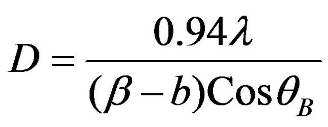
 (1)
(1)
where,  is the FWHM of the diffraction peak, λ is the wavelength of the incident CuK
  X-ray and
  is Bragg diffraction angle. b is standard instrumental broadening (0.08˚). The mean crystallite size of Ti:Cu3N is calculated by using strongest peak namely (100) peak (Table 2).
The presence of N neutrals reflected [30] from the single TiCu bi-component surface and impinging on the growing film with sufficient energy (due to large throw distance) can produce atomic scale heating in addition to substrate temperature which decompose the metastable Ti:Cu3N nano-crystallites to copper and escaped nitrogen [31]. This phenomenon becomes more significant at substrate temperature of 150˚C), because unbound N atoms out-diffuse from Ti:Cu3N crystallite into intercrystallite boundaries. The mean crystallite size of Ti:Cu3N for the samples prepared at substrate temperature of 150˚C has minimal value. It is due to N precipitation around the crystallites and suppression of their growth. As substrate temperature increases from 150˚C to 180˚C, extra N concentration at inter-crystallite boundaries produces driving force to transport N into Ti:Cu3N crystallite. As it is seen, the lattice constant and mean crystallite size of Ti:Cu3N increases up to substrate temperature of 180˚C.
3.2. Surface Morphology and Chemical Composition
Surface morphology of the nitrided Ti-Cu thin films

Figure 1. XRD pattern of nitrided Ti-Cu films at various substrate temperatures.
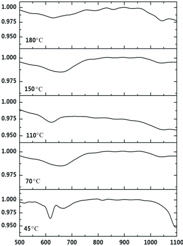
Figure 2. The FTIR spectra of nitrided Ti-Cu films deposited at various substrate temperatures.
deposited at substrate temperature are shown in Figure 3. The films have granular structure with clear grain structure and sharp grain boundaries. The extra nitrogen atoms that are not located at vacant interstitial site of Ti:Cu3N crystal structure or not trapped at crystallite boundaries diffuse into grain boundaries. This mechanism suppresses the agglomeration of grain because of N precipitation around them. Surface roughness of the films increases with increase in substrate temperature [32-35].
In order to estimate the atomic Ti:Cu ratio in films, we make the following assumptions:
• difference in throw distance of any sputtered component in target-substrate spacing;
• difference in nitriding kinetics on target surface of any component;
• difference in sticking coefficient of any sputtered component on substrate;
• re-sputtering contribution in altering the chemical composition due to the reflected N neutral and the sputtered Ti and Cu atoms collide with the growing film are excluded. The atomic Ti:Cu ratio can roughly be calculated by [25].
 (2)
(2)
where  is Ti concentration in target surface.
  is relative partial pressure of jth gas, j = N2 and Ar.
  is sputtering yield of ith atom due to jth species, I = Ti, Cu.

Figure 3. SEM images of the nitrided Ti-Cu films prepared at (a) 45˚C; (b) 70˚C; (c) 110˚C; (d) 150˚C; (e) 180˚C.
We assume  ion bombardment acts as same as two separate N+ ions with half energy. Sputtering yield is depending on energy and angular such as
 (3)
(3)
where E is the energy of incident ions and is approximately equal to 0.75 eVd [36]. θ is the ejection angle of sputtered atoms with respect to the surface normal. Energy dependent part is given by Eckstein et al. [37] as
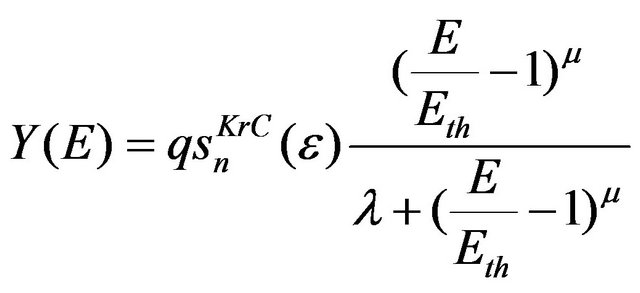 (4)
(4)
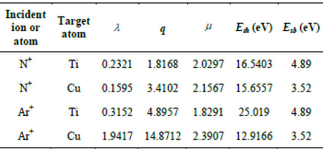
q, Eth,  and
and , which are material dependent parameters, listed in Table 3 for pairs of incident ion and target atom. Eth and
  are threshold energy for sputtering and nuclear stopping power, respectively.
Angular distribution of sputtered atom is proposed by Yamamura et al. [38] as heart shape
 (5)
(5)
where  is a fitting parameter. The fitting parameter depends on the mass and binding energy of the target material, mass and ion energy. It may be expressed as
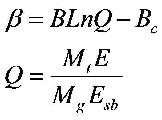 (6)
(6)
where Mt is the mass of the sputtered atom, Esb is binding energy of the sputtered material (Table 3). The values of B and Bc were respectively approximated as 0.488 and 2.44. The near normal ejection (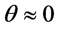 ) of Ti:Cu atomic ratio is nearly calculated 0.073 through Equation (2) for different substrate temperature. There is a good agreement between the calculated and experimental values for Ti:Cu atomic ratio (Table 2).
The atomic Ti:Cu ratio is shown in Table 2. As the substrate temperature increases, the atomic Ti:Cu ratio of the deposited films on Si (111) increases until 0.088 at 110˚C and then decreases. It seems by increasing substrate temperature to 110˚C, surface adsorption of Ti atoms increases. Afterward, re-evaporation of Ti atoms occurs (due to lower mass in comparison to Cu) from liquid phase in gas-liquid-solid growth mechanism of films that developed by Shaginyan et al. [39]. The Ti:Cu ratios are generally lower than atomic Ti:Cu ratio of original Ti13Cu78 target, namely 0.15. It was known that the near normal sputtering yield ratio of Ti to Cu is calculated 0.487 through Equation (4). Also, when Ti is sputtered in an Ar-N2 mixture atmosphere, the sputtering yield is decreased because a part of Ti on the target surface is nitrided [40]. This effect is weaker for the Cu because
Table 3. Materials dependent parameters presented by Eckstein et al. [37] for Ti and Cu target atoms bombarded by N and Ar ions.
it is more difficult to nitride Cu than Ti due to weaker Cu-N bonding. After being sputtered for some time the Ti:Cu ratio on the target surface will reach an equilibrium so that the ratio of the sputtered yield of the two materials are less than their ratio in the bulk target. Thus, it is likely that the difference between the composition in the target and film is caused by their different throw distance, nitriding kinetics, angular distribution of any sputtered component and different absorption rates on the film surface.
3.3 Optical Properties
There is an easy method for determination of optical constants, which depends on single transmittance measurement. The refractive index n and the extinction coefficient k as well as the thickness d of polycrystalline nitrided Ti-Cu thin films on thick quartz substrate were studied. They were determined from transmittance data only using PUMA approach and code described by Birgin et al. [41] used in our previous work [25,26,31]. Poelman et al. [42] have reviewed and tested PUMA approach and shown it to produce excellent estimate of optical constants of thin films.
The experimental transmittance data are compared with theoretical values, in PUMA code. The difference between the two values is minimized until a best solution is achieved for the refractive index n, the extinction coefficient k and the film thickness d. Deposition rate (R) has been calculated from the average film thickness at given deposition time (Table 2). The deposition rate is weakly depending on substrate temperature. Figures 4 and 5 show dispersion of the calculated refractive index n and extinction coefficient k as functions of wavelength. The absorption coefficient of Ti-Cu-N films is related to extinction coefficient through α = 4πk/λ (Figure 6).
The Ti:Cu3N lattice constant (Table 1) and the fundamental band-gap edge (from Figure 6) have the same trend vs. substrate temperature. These behaviors simultaneously illustrate the effects of N content and Ti addition in changing the lattice constant and absorption process.
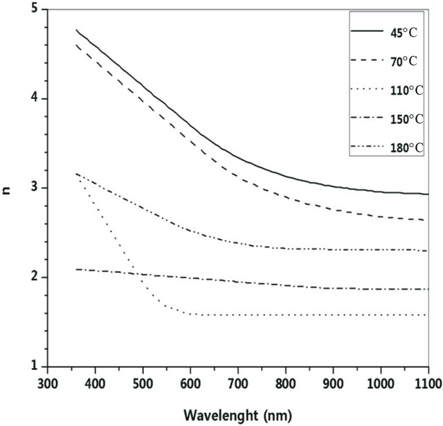
Figure 4. Dispersion of refractive index at various substrate temperatures.
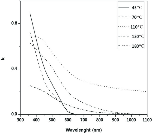
Figure 5. Dispersion of extinction coefficient at various substrate temperatures.
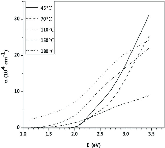
Figure 6. Variations of absorption coefficient with photon energy at various substrate temperatures.
3.4 Films Resistivity
There have been reports that the resistivity of Cu3N and Cu are 20 μΩcm - 2 103
103  cm and 1.75 - 2 μΩcm, respectively [32]. The resistivity of nitrided Ti-Cu films on glass slide at room temperature is presented in Table 2. The electrical conduction of films grown as the phase mixture (composite) of Ti:Cu3N nano-crystallite and Cu nanoparticle might follow the effective medium theory. Three simultaneous conduction mechanisms Ti:Cu3N semiconducting conduction, Cu metallic conduction and tunneling through crystallite boundary play important roles in carrier transport [31]. The nanocomposite resistivity is correlated to scattering dislocation inside crystallite (intra-crystallite boundary effect), scattering from potential barrier due to intercrystallites boundary effect and scattering through nanocrystallite boundary (size effect) [31].
4. Conclusion
Nitrided Ti-Cu thin films were grown on Si (111), glass slide and KBr substrates by reactive DC magnetron sputtering of a sintered Ti-Cu bi-component target. The asdeposited films on Si (111) substrate have composite structure of Ti:Cu3N nano-crystallite and metallic Cu nano-particle. The titanium atoms are positioned in the Cu3N crystal lattice and not segregated in other phases. The Ti addition causes to nitrogen excess; located at vacant interstitial site of Ti:Cu3N crystal structure, trapped at nano-crystallite and grain boundaries. The films have granular structure with clear grain boundaries. The atomic Ti:Cu ratio of films is less than that of the original target due to various differential sputtering yields, different throw distance and various sticking coefficient of any component. Refractive index, absorption coefficient and resistivity of the films are strongly dependent on substrate temperature and microstructural properties.
5. Acknowledgements
The corresponding author would like to acknowledge financial support of Iranian nanotechnology initiative. Also, he thanks Mohammad Safi Shalmazari from faculty of chemistry, university of Tabriz, for invaluable help. Also, he appreciates Department of Solid State and Electronics, Faculty of Physics, University of Tabriz, Tabriz, Iran.
REFERENCES
- J. Musil, “Magnetron Sputtering of Alloy and AlloyBased Films,” Thin Solid Films, Vol. 343-344, 1999, pp. 47-50. doi:10.1016/S0040-6090(98)01567-3
- Y. F. Ding and C. Alexander Jr., “Effects of Ti on N Distribution and Diffusion in FeTiN Thin Films,” IEEE Transactions on Magnetics, Vol. 42, No. 1, 2006, pp. 5- 11. doi:10.1109/TMAG.2005.860129
- J. F. Pierson, E. Tomasella and Ph. Bauer, “Reactively Sputtered Ti-B-N Nanocomposite Films: Correlation between Structure and Optical Properties,” Thin Solid Films, Vol. 408, No. 1-2, 2002, pp. 26-32. doi:10.1016/S0040-6090(02)00071-8
- P. Zeman, R. Cerstvy and P. H. Mayerhofer, “Structure and Properties of Hard and Superhard Zr-Cu-N Nanocomposite Coatings,” Materials Science and Engineering: A, Vol. 239, No. 1-2, 2000, pp. 189-197. doi:10.1016/S0921-5093(00)00917-5
- J. Musil and H. Polakova, “Hard Nanocomposite Zr-Y-N Coatings, Correlation between Hardness and Structure,” Surface and Coatings Technology, Vol. 127, No. 1, 2000, pp. 99-106. doi:10.1016/S0257-8972(00)00560-0
- N. N. Iosad, N. M. Van der Pers and S. Grachev, “Texture Formation in Sputter-Deposited (Nb0.7,Ti0.3)N Thin Films,” Journal of Applied Physics, Vol. 92, No. 9, 2002, p. 4999. doi:10.1063/1.1510589
- H. Maezawa, T. Sato and T. Noguchi, “Process Simulation of Reactive DC Magnetron Sputtering for Thin Film Deposition of Niobium-Titanium Nitride,” IEEE Transactions on Applied Superconductivity, Vol. 15, No. 2, 2005, pp. 3520-3523. doi:10.1109/TASC.2005.849027
- P. Scardi, Y. H. Dong and C. Tosi, “Co, Ni-Base Alloy Thin Films Deposited by Reactive Radio Frequency Magnetron Sputtering,” Journal of Vacuum Science & Technology A, Vol. 19, No. 5, 2001, p. 2394. doi:10.1116/1.1385907
- Z. L. Liu, X. G. Li and A. Y. Zuo, “Effect of N2-Gas Partial Pressure on the Structure and Properties of Copper Nitride Films by DC Reactive Magnetron Sputtering,” Plasma Science and Technology, Vol. 9, No. 2, 2007, p. 147. doi:10.1088/1009-0630/9/2/06
- M. Asano, K. Umeda and A. Tasaki, “Cu3N Thin Film for a New Light Recording Media,” Japanese Journal of Applied Physics, Vol. 29, 1990, pp. 1985-1986. doi:10.1143/JJAP.29.1985
- T. Maruyama and T. Morishita, “Copper Nitride and Tin Nitride Thin Films for Write-Once Optical Recording Media,” Applied Physics Letters, Vol. 69, 1996, p. 890. doi:10.1063/1.117978
- R. Cremer, M. Witthaut and D. Neuschutz, “Deposition and Characterization of Metastable Cu3N Layers for Applications in Optical Data Storage,” Microchimica Acta, Vol. 133, No. 1-4, 2000, pp. 299-302. doi:10.1007/s006040070109
- L. Maya, “Deposition of Crystalline Binary Nitride Films of Tin, Copper, and Nickel by Reactive Sputtering,” Journal of Vacuum Science & Technology A, Vol. 11, No. 3, 1993, p. 604. doi:10.1116/1.578778
- D. M. Borsa, S. Grachev, C. Presura and D. O. Boerma, “Growth and Properties of Cu3N Films and Cu3N/γ′- Fe4N Bilayers,” Applied Physics Letters, Vol. 80, No. 10, 2002, pp. 1823-1825. doi:10.1063/1.1459116
- U. Hahn and W. Weber, “Electronic Structure and Chemical-Bonding Mechanism of Cu3N, Cui3NPd, and Related Cu(I) Compounds,” Physical Review B, Vol. 53, No. 19, 1996, pp. 12684-12693. doi:10.1103/PhysRevB.53.12684
- M. G. Moreno-Armenta, W. L. Perez and N. Takeuchi, “First-Principles Calculations of the Structural and Electronic Properties of Cu3MN Compounds with M = Ni, Cu, Zn, Pd, Ag, and Cd,” Solid State Sciences, Vol. 9, No. 2, 2007, pp. 166-172. doi:10.1016/j.solidstatesciences.2006.12.002
- J. Wang, J. T. Chen, X. M. Yuan, Z. G. Wu, B. B. Miao and P. X. Yan, “Copper Nitride (Cu3N) Thin Films Deposited by RF Magnetron Sputtering,” Journal of Crystal Growth, Vol. 286, No. 2, 2006, pp. 407-412. doi:10.1016/j.jcrysgro.2005.10.107
- K. V. S. Reddy, S. S. Reddy, P. S. Reddy and S. Uthana, “Copper Nitride Films Deposited by Dc Reactive Magnetron Sputtering,” Journal of Materials Science: Materials in Electronics, Vol. 18, No. 10, 2007, pp. 1003-1008. doi:10.1007/s10854-007-9120-0
- G. H. Yue, P. X. Yan, J. Z. Liu, M. X. Wang, M. Li and X. M. Yuan, “Copper Nitride Thin Film Prepared by Reactive Radio-Frequency Magnetron Sputtering,” Journal of Applied Physics, Vol. 98, No. 10, 2005, Article ID: 103506. doi:10.1063/1.2132507
- N. Gordillo, R. Gonzalez-Arrabal, A. Alvarez-Herrero and F. Agullo-Lopez, “Free-Carrier Contribution to the Optical Response of N-Rich Cu3N Thin Films,” Journal of Physics D: Applied Physics, Vol. 42, No. 16, 2009, Article ID: 165101. doi:10.1088/0022-3727/42/16/165101
- T. Maruyama and T. Morishita, “Copper Nitride Thin Films Prepared by Radio-Frequency Reactive Sputtering,” Journal of Applied Physics, Vol. 78, No. 6, 1995, pp. 4104-4107. doi:10.1063/1.359868
- K. J. Kim, J. H. Kim and J. H. Kang, “Structural and Optical Characterization of Cu3N Films Prepared by Reactive RF Magnetron Sputtering,” Journal of Crystal Growth, Vol. 222, No. 4, 2000, pp. 767-772. doi:10.1016/S0022-0248(00)00968-4
- Y. Du, A. L. Ji, L. B. Ma, Y. Q. Wang and Z. X. Cao, “Electrical Conductivity and Photoreflectance of Nanocrystalline Copper Nitride Thin Films Deposited at Low Temperature,” Journal of Crystal Growth, Vol. 280, No. 3-4, 2005, pp. 490-494. doi:10.1016/j.jcrysgro.2005.03.077
- J. F. Pierson and D. Horwat, “Addition of Silver in Copper Nitride Films Deposited by Reactive Magnetron Sputtering,” Scripta Materiala, Vol. 58, No. 7, 2008, pp. 568- 570. doi:10.1016/j.scriptamat.2007.11.016
- A. Rahmati, H. Bidadi, K. Ahmadi and F. Hadian, “Ti Substituted Nano-Crystalline Cu3N Thin Films,” Journal of Coatings Technology and Research, Vol. 8, No. 2, 2011, pp. 289-297. doi:10.1007/s11998-010-9279-9
- A. Rahmati, “Reactive DC Magnetron Sputter Deposited Ti-Cu-N Nano-Composite Thin Films at Nitrogen Ambient,” Vaccum, Vol. 85, No. 9, 2011, pp. 853-860. doi:10.1016/j.vacuum.2010.12.010
- J. F. Pierson, D. Wiederkehr and A. Billard, “Reactive Magnetron Sputtering of Copper, Silver, and Gold,” Thin Solid Films, Vol. 478, No. 1-2, 2005, pp. 196-205. doi:10.1016/j.tsf.2004.10.043
- I. S. Kim and P. N. Kumta, “Hydrazide Sol-Gel Process: A Novel Approach, for Synthesizing Nanostructured Titanium Nitride,” Materials Science and Engineering: B, Vol. 98, No. 2, 2003, pp. 123-134. doi:10.1016/S0921-5107(02)00595-0
- B. Subramanian, K. Ashok and M. Jayachandran, “Effect of Substrate Temperature on the Structural Properties of Magnetron Sputtered Titanium Nitride Thin Films with Brush Plated Nickel Interlayer on Mild Steel,” Applied Surface Science, Vol. 255, No. 5, 2008, pp. 2133-2138. doi:10.1016/j.apsusc.2008.07.083
- Z. Wang, S. A. Cohen, D. N. Ruzic and M. Goeckner, “Nitrogen Atom Energy Distribution in a Hollow-Cathode Planar Sputtering Magnetron,” Journal of Physical Review E, Vol. 61, No. 2, 2000, pp. 1904-1911.
- A. Rahmati, H. Bidadi, K. Ahmadi and F. Hadian, “Reactive DC Magnetron Sputter Deposited Titanium-CopperNitrogen Nano-Composite Thin Films with an Argon/ Nitrogen Gas Mixture,” Plasma Science and Technology, Vol. 12, No. 6, 2010, pp. 1-7. doi:10.1088/1009-0630/12/6/09
- J. F. Pierson, “Structure and Properties of Copper Nitride Films Formed by Reactive Magnetron Sputtering,” Vacuum, Vol. 66, No. 1, 2002, pp. 59-64. doi:10.1016/S0042-207X(01)00425-0
- X. Y. Fan, Z. G. Wu and G. A. Zhang, “Ti Dopped Copper Nitride Films Deposited by Cylindrical Magnetron Sputtering,” Journal of Alloys and Compounds, Vol. 440, 2007, p. 54.
- J. L. Vossen and W. Kern, “Thin Film Process II,” Academic Press, New York, 1991, pp. 181-186.
- J. A. Thornton, “The Microstructure of Sputter-Deposited Coatings,” Journal of Vacuum Science & Technology A, Vol. 4, No. 6, 1986, pp. 3059-3065. doi:10.1116/1.573628
- S. Mahieu and D. Depla, “Reactive Sputter Deposition of TiN Layers: Modelling the Growth by Characterization of Particle Fluxes towards the Substrate,” Journal of Physics D: Applied Physics, Vol. 42, No. 5, 2009, Article ID: 053 002. doi:10.1088/0022-3727/42/5/053002
- R. Behrisch and W. Eckstein, “Sputtering by Particle Bombardment, Experiments and Computer Calculations from Threshold to MeV Energies,” Spriger, New York, 2007.
- Y. Yamamura, T. Takiguchi and M. Ishida, “Energy and Angular Distributions of Sputtered Atoms at Normal Incadence,” Radiation Effects and Defects in Solids, Vol. 118, No. 3, 1991, pp. 237-261. doi:10.1080/10420159108221362
- L. R. Shaginyan, Y. I. Kim, J. G. Han, N. V. Britun, J. Musil and I. V. Belousov, “Novel Model for Film Growth Based on Surface Temperature Developing during Magnetron Sputtering,” Surface and Coatings Technology, Vol. 202, No. 3, 2007, pp. 486-493. doi:10.1016/j.surfcoat.2007.06.016
- M. Delfino, J. A. Fair and D. Hodul, “X-Ray Photoemission Spectra of Reactively Sputtered TiN,” Journal of Applied Physics, Vol. 71, 1992, pp. 6079-6085. doi:10.1063/1.350465
- E. G. Birgin, I. Chambouleyron and J. M. Martınez, “Estimation of the Optical Constants and the Thickness of Thin Films Using Unconstrained Optimization,” Journal of Computational Physics, Vol. 151, No. 2, 1999, pp. 862-990. doi:10.1006/jcph.1999.6224
- D. Poelman and P. F. Smet, “Methods for the Determination of the Optical Constants of Thin Films from Single Transmission Measurements: A Critical Review,” Journal of Physics D: Applied Physics, Vol. 36, No. 15, 2003, p. 1850. doi:10.1088/0022-3727/36/15/316