Crystal Structure Theory and Applications
Vol. 2 No. 2 (2013) , Article ID: 33276 , 5 pages DOI:10.4236/csta.2013.22009
Dichroic Electro-Optical Behavior of Rhenium Sulfide Layered Crystal
Graduate Institute of Applied Science and Technology, National Taiwan University of Science and Technology, Taipei, Taiwan
Email: chho@mail.ntust.edu.tw
Copyright © 2013 Ching-Hwa Ho. This is an open access article distributed under the Creative Commons Attribution License, which permits unrestricted use, distribution, and reproduction in any medium, provided the original work is properly cited.
Received December 3, 2012; revised January 4, 2013; accepted January 15, 2013
Keywords: Triclinic Crystals; Optical Materials; Polarization-Sensitive Devices
ABSTRACT
Dichroic behaviors of layered ReS2 have been characterized using angular dependent polarized-absorption and resistivity measurements in the van der Waal plane. The angular dependent optical and electrical measurements are carried out with angles ranging from q = 0˚ (E || b) to q = 90˚ (E ^ b) with respect to the layer crystal’s b-axis. The angular dependence of polarized energy gaps of ReS2 shows a sinusoidal variation of energies from ~1.341 eV (E || b) to ~1.391 eV (E ^ b). The experimental evidence of polarized energy gap leaves ReS2 a potential usage for fabrication of a polarized optical switch suitable for polarized optical communication in near-infra-red (NIR) region. Angular dependence of resistivities of ReS2 in the van der Waal plane has also been evaluated. The relationship of in-plane resistivities shows a sinusoidal-like variation from q = 0˚ (E || b) to 90˚ (E ^ b) and repeated periodically to 360˚. The experimental results of optical and electrical measurements indicated that ReS2 is not only an optical-dichroic layer but also an electrical-dichroism material presented in the layer plane.
1. Introduction
Dichroism and optical-anisotropic materials played an important role for the evolution of light-wave optics in past years. For generation of polarized light, dichroic crystal or birefringent solid is the most commonly used material because the specific axial anisotropy exists in the crystal structure. Among the dichroic or birefringent solids, the mineral tourmaline such as NaFe3B3Al6Si6O27(OH)4 or the birefringent crystal such as Calcite (CaCO3) are usually the crucial substances for making linear polarizers [1]. Such kinds of polarizers are usually suitable for making visible-to-ultraviolet lasers or for fabrication of linearly polarized devices.
Dichroic semiconductor¾rhenium disulfide (ReS2) has been synthesized and proposed to possess the potential capability for fabrication of polarization sensitive photodetector applied in multi-channel optical communications [2]. The polarization sensitive behavior of ReS2 is arisen from its specific in-plane optical anisotropy in the layer [2]. The crystallography of ReS2 is usually crystallized in a distorted CdCl2 layer-type structure with triclinic symmetry (space group P ) [3-5]. ReS2 is an indirect semiconductor with an unpolarized gap of about 1.37 eV [5]. From the observation of polarization-dependent spectral quantum efficiency, the layered ReS2 presents optically biaxial behavior with the linearly polarized lights incident normal to the basal plane [i.e. E || (001) and k ^ (001)] [6]. Polarized photocurrent measurements of an ITO/ReS2 device with different azimuthal angles revealed that angular dependence of photoresponses in ReS2 follows the Malus law [1,6]. The polarization-dependent spectral quantum efficiency also verified ReS2 an effective polarization sensitive photodetector applied in visible range [6].
In this paper, the optical and electrical dichroic properties of ReS2 are shown to simultaneously present in the van der Waal plane. The dichroic behaviors of ReS2 are characterized by angular dependent polarized-absorption and electrical-resistivity measurements in the layer plane. The measurements were done in the angular range from q = 0˚ (E || b) to q = 90˚ (E ^ b) with respect to the b-axis of the layer crystal. The polarized energy gaps of ReS2 were obtained from the analysis of polarization-dependent absorption spectra. The relation of the polarized gaps of ReS2 was determined to be Eg(q) = 1.366 − 0.025·cos(2q) eV. Angular dependence of resistivities of ReS2 in the van der Waal plane showed a sinusoidal-like variation from q = 0˚ (E || b) to q = 90˚ (E ^ b). The angular dependency of in-plane resistivities of ReS2 is r(q) = 21.054 − 14.535×cos(2q) W-cm. The optical and electrical evidences showed that ReS2 is not only an optical-dichroic layer but also an electrical-dichroism crystal in the van der Waal plane.
2. Experimental Procedure
2.1. Growth and Structural Property
Single crystals of ReS2 were grown by chemical vapor transport (CVT) method [7] using ICl3 as a transport agent. The growing process of ReS2 using CVT had been described elsewhere [8]. The as-grown crystals of ReS2 were essentially layer type. X-ray diffraction measurement confirmed triclinic structure of the crystal [8]. Weak van der Waals bonding between the layers means that they display good cleavage property parallel to the layers. The strong bonding force along the Re cluster chains also implies that we can easily tear the layer along b-axis via the auxiliary of weak bonding force between the individual chains. Hall effect measurement revealed p-type semiconducting behavior of the layer. The carrier density is ~1×1016 cm−3.
2.2. Optical Measurement
Measurements of reflectance and transmittance at nearnormal incidence were made on a scanning monochromatic measurement system. An 150 W tungsten-halogen lamp filtered by a PTI 0.2 m monochromator provided the monochromatic light. Transmission intensity was closely monitored to obtain an incidence as close to 90˚ as possible. Single crystals with a thickness of about 100 mm were used in the transmission measurements. The reflected light of the sample was detected by an EG & G type HUV-2000B silicon photodiode and the signal was recorded from an EG & G model 7265 dual phase lock-in amplifier. A pair of OPTOSIGMA near-infrared-dichroic-sheet polarizers with the measurement range of 760 - 2000 nm was employed in the polarization dependent optical measurements.
2.3. Electrical Measurement
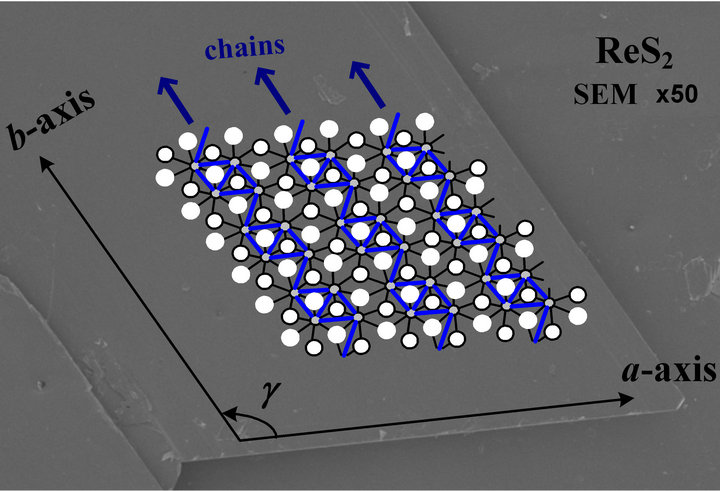
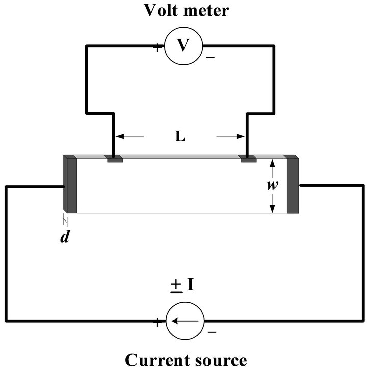
Angular dependent resistivity measurements of layered ReS2 were made on ten different samples cut in bar type. The cutting edge of each sample was varied from q = 0˚ (||b) to q = 90˚ (^b) with an angle increment of 10˚ starting from the layer crystal’s b-axis. Displayed in Figure 1(a) is a scanning-electron microscope (SEM) photograph of ReS2 in the layered plane. The crystal image is 50 × amplification and the crystal orientation of b-axis is shown. The b-axis is parallel to the metal Re cluster
 (a)
(a)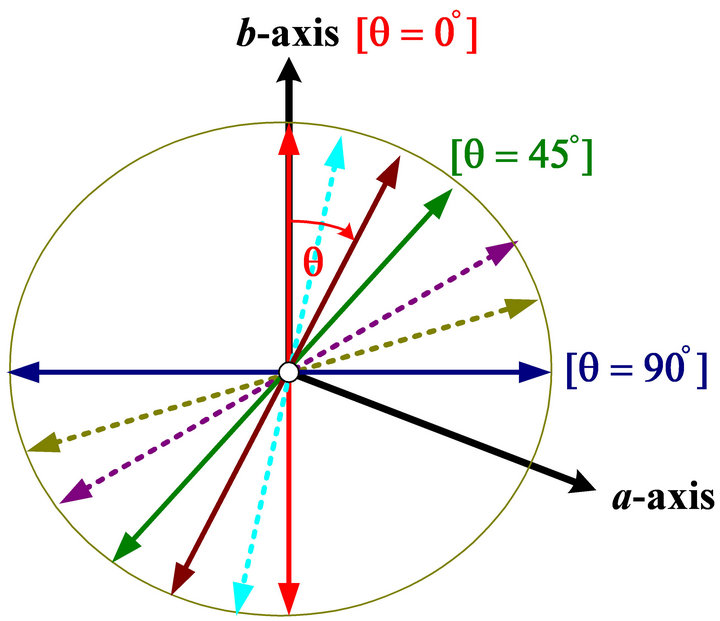 (b)
(b)
Figure 1. (a) SEM image of layered ReS2 on the van der Waal plane, where the Re4 clustering chains that corresponding to the crystal orientation of b-axis are illustrated. (b) Schematic illustrations for the angular dependent optical-absorption and electrical-resistivity measurements. The angle q is defined as the angular difference between the orientation of electric field and that of the crystal’s b-axis.
chains, which corresponds to the longest edge of the plate [6,9]. The angular dependence of electrical-resistivity and polarized-absorption measurements of ReS2 was evaluated by the rotation indication as shown in Figure 1(b). All the measurements were carried out with the angular range starting from q = 0˚ to q = 90˚. The angular increment of the polarized-absorption measurement is 5˚ while the increment is 10˚ for the electricalresistivity measurement.
3. Results and Discussion
3.1. Dichroic Optical Property
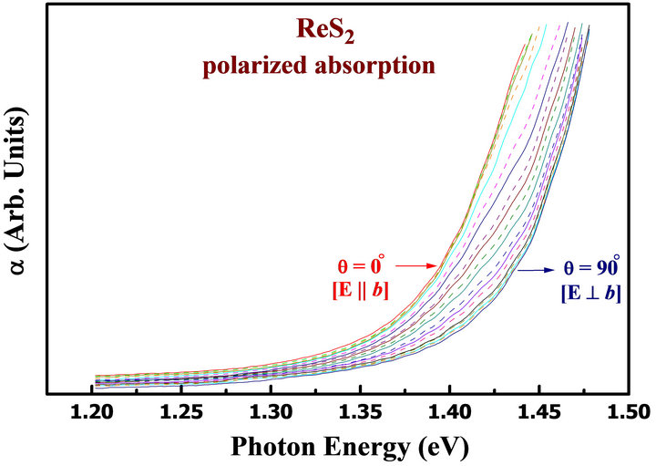
Polarized optical-absorption measurements were implemented with the polarization angles from q = 0˚ to q = 90˚. Absorption coefficient a of ReS2 can be determined from the transmittance Tr by taking into account the spectral dependence of the reflectance R using the relation 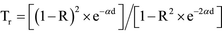 [10]. This equation assumes that there are multiple reflections within the sample, but that they add incoherently due to sample inhomogeneity or a sufficiently large spread of the incident angles. Because ad is large for the sample crystals, the second term in the denominator of the Tr relation can be neglected. Figure 2(a) displays the polarized absorption coefficients of ReS2 as a function of photon energy from q = 0˚ to q = 90˚ at 300 K. The absorption edges of ReS2 clearly indicate an energy blue-shift behavior with the increase of polarization angles from q = 0˚ to 90˚. The absorption-edge anisotropy in rhenium disulfide provides relevant evidence that the energy gap of ReS2 is polarization dependent. This property also lends a potential ability for ReS2 to fabricate a polarized optical switch suitable for polarized optical communication in the NIR region. The analysis of the experimental results in Figure 2(a) also shows that the absorption coefficient a for ReS2
 (a)
(a)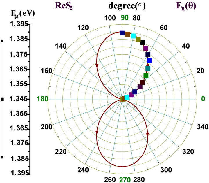 (b)
(b)
Figure 2. (a) Angular dependent polarized-absorption spectra of ReS2 from q = 0˚ to q = 90˚ with an angular increment of 5˚ at 300 K. (b) The angular dependency of polarized energy gaps of ReS2 in polar-coordination plot. The solid squares are the experimental data points and the solid lines are least-square fits to Equation (1). A double circle line that moving from q = 0˚ to 360˚ depicts the varying trace of the polarized energy gaps for layered ReS2.
is proportional to (hn-Eg)n with n = 2.0 ± 0.1. This suggests an indirect allowed transition. A more complete analysis by taking into account both absorption and emission phonons [5] could be utilized to determine the polarized band gaps and average phonon energies from the polarized absorption spectra. Shown in Figure 2(b) by the solid squares (in polar-coordination plot) are the values of polarized energy gaps of ReS2 ranging from q = 0˚ to q = 90˚ with an increment of 5˚. The average phonon energies for the indirect ReS2 from the polarized absorption spectra are determined to be about 25 ± 5 meV. The angular dependence of polarized energy gaps of ReS2 shows a sinusoidal-like variation of energies from 1.341 eV (q = 0˚) to 1.391 eV (q = 90˚). The angular dependence of the polarized gaps of ReS2 can be analyzed by fitting the experimental data to a sinusoidal functional form of
 (1)
(1)
where Eg0 is related to the unpolarized band gap, and
 is the energy amplitude of the sinusoidal variation.
The energy-variation relation of Equation (1) is similar to the generalized Malus law [11] that describing the dependence of the linearly polarized lights. The solid curve displayed in Figure 2(b) is the results by fitting the polarized energy gaps to Equation (1). From the leastsquare fits using Equation (1), the energy values of 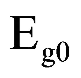 and
and  are determined to be 1.366 eV and 0.025 eVrespectively. As shown in Figure 2(b), a polar-coordination plot of a double circle line just depicts the curve trace of the polarized gaps moving from q = 0˚ to 360˚ for the layered ReS2. This result concludes that the energy variation of polarized energy gaps for a dichroic semiconductor also follows the generalized Malus rule.
3.2. Axial Dependence of Electrical Carrier Transport
The dichroic electrical property of the p-type layered ReS2 in van der Waal plane was studied using a regular four-point method [12]. The measurement configuration is shown in Figure 3(a). A dc current source supplied the current and a dc voltmeter used for detection unit. The in-plane resistivities were measured on ten different rectangular shape samples with different orientations. The direction of cutting-edge for each specimen was varied from q = 0˚ (|| b) to q = 90˚ (^ b) with an angular increment of 10˚. Displayed in Figure 3(b) by the solid circles are the experimental data points for the angular dependent in-plane resistivities of layered ReS2. The in-plane electrical anisotropy of ReS2 in Figure 3(b) clearly indicates the lowest resistivity is occurred with the electric field parallel to the b-axis while the maximum resistivity is arisen along the direction perpendicular to b-axis. The
 (a)
(a)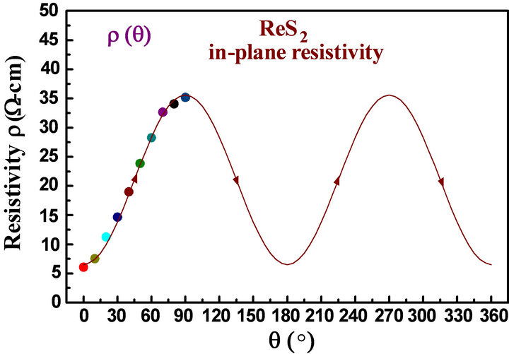 (b)
(b)
Figure 3. (a) Measurement configuration of electrical resistivity using regular four-point method. (b) Angular dependent in-plane resistivities of ReS2. The solid circles are the data points measured from q = 0˚ to q = 90˚. The solid curve is the fitting result extended from 0° to 360˚.
lowest value of resistivity along b-axis is related to the strongest bonding force existed along the crystal orientation of the Re cluster chains. The angular-dependent in-plane resistivities of ReS2 in Figure 3(b) also reveal a sinusoidal-like variation from q = 0˚ (E || b) to q = 90˚ (E ^ b). The relationship of angular dependent resistivities of ReS2 can also be analyzed by using the generalized Malus formula of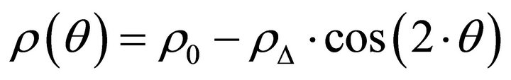 . The solid curve in Figure 3(b) is the fitting result of angular-dependent in-plane resistivities of ReS2 extended from 0˚ to 360˚. The angular dependence of in-plane resistivities of ReS2 is determined to be r(q) = 21.054 − 14.535·cos(2q) W-cm. The electric anisotropy in Figure 3(b) confirms that ReS2 is an electrical dichroism which presents a special axial selectivity of electrical conduction along the layer plane. This property is attributed to the in-plane axial anisotropy of mobilities that existed in the triclinic-layered ReS2.
4. Conclusion
In conclusion, the dichroic optical and electrical behaveiors of layered ReS2 were characterized using angular dependent polarized-absorption as well as electrical-resistivity measurements in the van der Waal plane. The polarized energy gaps of ReS2 show a sinusoidal angular dependence of Eg(q) = 1.366 − 0.025·cos(2q) eV. The in-plane resistivities of ReS2 were measured on ten different rectangular-shape samples with dissimilar orientations. The angular dependent in-plane resistivities of ReS2 also show a sinusoidal-like variation from q = 0˚ (E || b) to q = 90˚ (E ^ b). The relationship of angular dependent resistivities of ReS2 was determined to be r(q) = 21.054 − 14.535·cos (2q) W-cm. The angular dependence of resistivity is due to the in-plane axial anisotropy of mobilities in the triclinic-layered ReS2. The experimental observations verified that ReS2 is not only an optical-dichroic layer but also an electrical dichroism in the van der Waal plane.
5. Acknowledgements
The author would like to acknowledge the research funding supported by the National Science Council of Taiwan under the Project No. NSC 101-2221-E-011-052- MY3.
REFERENCES
- E. Hecht, “Optics,” 4th Editon, Addison Wesley, San Francisco, 2002, p. 333.
- C. H. Liang, K. K. Tiong, Y. S. Huang, D. Dumcenco and C. H. Ho, “In-Plane Anisotropic Electrical and Optical Properties of Gold-Doped Rhenium Disulphide,” Journal of Materials Science: Materials in Electronics, Vol. 20, No. 1, 2009, pp. S476-S479. doi:10.1007/s10854-008-9685-2
- J. C. Wildervanck and F. Jellinek, “The Dichalcogenides of Technetium and Rhenium,” Journal of the Less Common Metals, Vol. 24, No. 1, 1971, pp. 73-81. doi:10.1016/0022-5088(71)90168-8
- H. -J. Lamfers, A. Meetsma, G. A. Wiegers, and J. L. de Boer, “The Crystal Structure of Some Rhenium and Technetium Dichalcogenides,” Journal of Alloys and Compounds, Vol. 241, 1996, pp. 34-39.
- C. H. Ho, P. C. Liao, Y. S. Huang, T. R. Yang and K. K. Tiong, “Optical Absorption of ReS2 and ReSe2 Single Crystals,” Journal of Applied Physics, Vol. 81, No. 9, 1997, pp. 6380-6383. doi:10.1063/1.365357
- K. Friemelt, M.-Ch. Lux-Steiner and E. Bucher, “Optical Properties of the Layered Transition-Metal-Dichalcogenide ReS2: Anisotropy in the van der Waals Plane,” Journal of Applied Physics, Vol. 74, No. 8, 1993, pp. 5266-5268. doi:10.1063/1.354268
- C. H. Ho, “Single Crystal Growth and Characterization of Copper Aluminum Indium Disulfide Chalcopyrites,” Journal of Crystal Growth, Vol. 317, No. 1, 2011, pp. 52-59. doi:10.1016/j.jcrysgro.2011.01.008
- C. H. Ho, Y. S. Huang, P. C. Liao and K. K. Tiong, “Crystal Structure and Band-Edge Transitions of ReS2-xSex Layered Compounds,” Journal of Physics and Chemistry of Solids, Vol. 60, No. 11, 1999, pp. 1797- 1804. doi:10.1016/S0022-3697(99)00201-2
- B. A. Parkinson, J. Ren and M.-H. Whangbo, “Relationship of STM and AFM Images to Local Density of States in Valence and Conduction Bands of ReS2,” Journal of the American Chemical Society, Vol. 113, No. 21, 1991, pp. 7833-7837. doi:10.1021/ja00021a001
- J. I. Pankove, “Optical Processes in Semiconductors,” Dover, New York, 1975.
- G. A. Medvedkin, Yu. V. Rud and M. A. Tairov, “Photoelectric Anisotropy of II-IV-V2 Ternary Semiconductors,” Physica Status Solidi (a), Vol. 115, No. 1, 1989, pp. 11- 50. doi:10.1002/pssa.2211150102
- H. H. Wieder, “Laboratory Notes on Electrical and Galvanomagnetic Measurements,” Elsevier, Amsterdam, 1979.