Optics and Photonics Journal
Vol.08 No.04(2018), Article ID:84267,11 pages
10.4236/opj.2018.84011
Demonstration of an As2S3 Grating Coupler on Thin Film LiNbO3
Chen Zhang, Christi K. Madsen
Department of Electrical and Computer Engineering, Texas A&M University, College Station, TX, USA

Copyright © 2018 by authors and Scientific Research Publishing Inc.
This work is licensed under the Creative Commons Attribution International License (CC BY 4.0).
http://creativecommons.org/licenses/by/4.0/


Received: January 8, 2018; Accepted: April 27, 2018; Published: April 30, 2018
ABSTRACT
We present both design and experimental results for an As2S3 grating coupler on a thin film LiNbO3 substrate. A basic grating coupler structure is designed with coupling efficiency of 53% to a single mode fiber. A maximum simulated coupling efficiency of 78.8% is achieved, assuming a polymer bonding process. The basic structure was fabricated, and the coupling efficiency was measured to be at least 23.4% at 1540 nm. Some of the loss may be attributable to non-grating sources, such as waveguide tapers and testing fiber tails. A grating cavity was then measured using the grating couplers. The cavity waveguide propagation loss was 2.0 dB/cm. For a 400 nm thick As2S3 on 500 nm thin film LiNbO3 on insulator, the confinement factor in the LiNbO3 crystal is 82.3% when the As2S3 waveguide width is 400 nm, showing that As2S3-on-thin film LiNbO3 is an excellent candidate for thin film electro-optic applications.
Keywords:
Thin Film Lithium Niobate, Arsenic Trisulfide Waveguide, Grating Coupler, Grating Cavity

1. Introduction
Lithium niobate (LiNbO3) has been widely used in high-speed modulators and phased arrays due to the excellent electro-optic properties of LiNbO3 material [1] [2] . Compared with Si platform, LiNbO3 platform features high bandwidth and good temperature stability [3] [4] .
Thin film LiNbO3 furthers the advantage over traditional LiNbO3 by confining mode in vertical direction. Thin film LiNbO3 is produced through ion implantation, to create crystal damage at the desired depth of bulk LiNbO3 wafer, followed by wet etching or thermal annealing [5] [6] . The technology development of thin film LiNbO3 enables ultra-compact electro-optic (EO) devices such as modulators and switches [5] [7] [8] .
Arsenic trisulfide (As2S3) waveguide on LiNbO3 crystal is a hybrid platform for both near-infrared (near-IR) and mid-infrared (mid-IR). With certain waveguide width and thickness values, optical mode inside the waveguide partially overlaps with LiNbO3 crystal, enabling EO applications. Since standard semiconductor fabrication techniques can be applied to As2S3 patterning, different As2S3 structures including sidewall Bragg grating [9] and ring resonator [10] have been reported.
Coupling light between this platform and the external light source and detector should be carefully designed, in order to avoid excessive mode mismatch loss. In order to couple light into and out of different As2S3 structures, a grating coupler can be used. Reference [11] has focused on the design method of As2S3 grating coupler on bulk LiNbO3 substrate. In this paper, design, fabrication and measurement of As2S3 grating coupler on top of thin film LiNbO3 crystal are discussed in details.
2. Device Design
Figure 1 illustrates an As2S3 grating coupler on thin film LiNbO3 with both top view and side view. Here, wGC is the grating coupler width. Λ stands for the grating coupler period. d is the length of the grating section within each period. t is the grating coupler thickness. The grating coupler duty cycle (DC) is defined as d/Λ.
Light diffraction in a grating coupler follows phase matching condition. The goal of grating coupler design is to maximize the coupling efficiency between the first order light diffraction at the coupler output and a single-mode fiber (SMF) mode. Equation (1) is the grating coupler equation that builds connection between the first order diffraction angle θ and the effective refractive index of the grating coupler neff [9] . Here, Λ is grating coupler period, λ is wavelength of light, and nc is cladding refractive index.
. (1)
Effective refractive index of a grating coupler is determined by the material refractive index and thickness of each layer, as well as grating coupler DC. In simulation, we use 500 nm as LiNbO3 thin film thickness and 2 μm as SiO2 layer thickness, which is used in device fabrication. Table 1 lists the refractive index of each layer at 1550 nm [12] . It is worth noting that extraordinary refractive index of LiNbO3 is used, since this design is carried out for TE polarization on X-cut thin film LiNbO3 and the light propagation is along Y-axis.
There are more than one set of parameters satisfies (1), each of which results in a first diffraction field. Fimmprop (from Photon Design Inc.) is used to simulate grating coupler output field, and Python scripting is used to calculate and maximize the overlapping integral between the grating coupler output field and the Gaussian approximation in a SMF. The coupling angle is set to 12˚. The

Figure 1. Top view and side view of As2S3 grating coupler on thin film LiNbO3.

Table 1. Refractive index for each material in grating coupler design.
cladding index is set to 1.444, since SiO2 is used as cladding material. The target wavelength is 1550 nm. After optimization, grating coupler period is 850 nm, its thickness is 400 nm and its DC is 0.59. In order to further increase coupling efficiency, DC in the first several periods of the grating coupler can be tweaked (also named apodization) in order to make the grating coupler output field more resembles Gaussian approximation in a SMF [13] . After optimization, DC = 0.88 for the first two periods; DC = 0.82 for the next two periods; DC = 0.70 for the next two periods; DC = 0.59 (unchanged) for the rest 10 periods. Compared to the uniform grating coupler, the coupling efficiency is further increased from 27.5% to 53.0%. Figure 2 shows this basic As2S3 grating coupler structure.
The above design methodology can be carried out targeting mid-infrared application. The optimized mid-infrared structure would have different grating period, duty cycle, and material thickness compared to above design.
Figure 3(a) shows periodicity of coupling efficiency with respect to SiO2 buffer layer thickness. The fine thickness control of this SiO2 buffer layer is critical for constructive interference between the top and bottom diffractive light. Figure 3(b) is the spectral response of the basic grating coupler. The 3-dB bandwidth of the basic grating coupler is 46 nm.
Further improvements on top of the basic grating coupler structure in terms of coupling efficiency to a SMF require substantially changing the structure. One way is to introduce a Bragg reflector between substrate and grating coupler to reduce substrate leakage [13] . In our case, SiO2 can be used as low-index material and As2S3 can be used as high-index material. Another way to improve the grating coupler performance is to control As2S3 etching time for a specific grating depth, in order to reduce undesirable light reflection.
Since additional layers are required between LiNbO3 thin film and substrate, this improved grating coupler consists of two parts: the first part is Bragg reflector layers on a substrate; the second part is similar to the basic grating coupler

Figure 2. Basic As2S3 grating coupler structure.
 (a)
(a)  (b)
(b)
Figure 3. (a) (left) Coupling efficiency periodically changes with SiO2 buffer thickness; (b) (right) Grating coupler spectral response for the basic structure.
structure. A bonding step brings these two parts together. Figure 4 shows the improved structure implementing a Bragg reflector and controlled As2S3 etching.
Benzocyclobutene (BCB) can be used as the bonding polymer. BCB is widely applied to low temperature wafer level bonding, with good adhesion, easy fabrication, repeatable thickness and refractive index control [14] [15] . According to Dow Chemical Company documents [16] , Cyclotene (3022-46) should be used, with curing temperature 250˚C for 60 minutes. This polymer possesses pretty good thermal stability below 350˚C. The film refractive index after curing is 1.535 at 1550 nm.
Optical simulation of the improved grating coupler structure is carried out in Fimmprop. After optimization, the coupling efficiency is 78.8% at 1550 nm for TE polarization. The design parameters are listed in Table 2.
Figure 5 shows the grating coupler spectral response at coupling angle of 14˚. The solid curve is the spectral response of the improved structure with Bragg reflector on the bottom, while the dashed curve is the spectral response of the same grating parameters without Bragg reflector. It is worth noting that the peak coupling efficiency (80.6%) is at 1545 nm rather than 1550 nm, because there are a lot of variables for the design, and each variable is discrete in the simulation with practical considerations. The apodization design makes the spectrum asymmetrical. The 3-dB bandwidth is 60 nm, defined by two 3-dB drop points

Figure 4. Improved As2S3 grating coupler structure.

Figure 5. Grating coupling efficiency with reflector and without reflector.
Table 2. Design parameters of the improved As2S3 grating coupler.
a. For the first two periods, DC = 0.94; for the next two periods, DC = 0.82; then the next two DC = 0.70; for the rest 16 periods, DC = 0.59.
from the efficiency peak. Spectrum symmetry can be further optimized by tweaking grating period.
3. Fabrication
A thin film X-cut LiNbO3 sample (from NanoLN) is cleaned using a Q-tip with acetone, methanol and isopropyl alcohol (IPA). This sample has 500 nm X-cut thin film LiNbO3 on top of 2 μm SiO2 on Si substrate. We sputter 400 nm As2S3, 130 nm SiO2 and 40 nm Ti onto the sample. Then electron beam lithography (EBL) is performed for pattern definition. 2.25% PMMA solution is used as positive EBL resist. The exposure dosage is 350 μC/cm2. After EBL, the sample is developed in fresh developer that is made from 40 mL IPA and 20 mL DI water. O2 Plasma ashing is then carried out to remove the residue PMMA resist at corner areas. 30 nm of Ti is deposited through e-beam evaporation, followed by a lift-off step in acetone.
Reactive ion etching (RIE) is performed to remove the metal layer and As2S3 outside pattern areas. In order to make sure As2S3 patterns are preserved, the sample needs to be taken out and checked under a microscope several times throughout RIE. After RIE, 100 nm SiO2 is sputtered as a protective layer. A complete fabrication flow chart is shown in Figure 6.
In comparison, the improved structure is much more complicated. Figure 7 shows a tentative fabrication flow chart. Here, the top part of grating coupler starts with As2S3 deposition (along with SiO2 and Ti protective layer deposition) on LiNbO3 thin film substrate. Then EBL is used to define grating coupler pattern. During RIE step, the etching time should be controlled so that the shallow layer has 400 nm As2S3 removed, while the pattern area preserve the 500 nm As2S3. The bottom part starts with deposition of As2S3 and SiO2 thin films as the Bragg reflector, following Table 2. Then the BCB solution is spin-coated and curing temperature 250˚C for 60 minutes. Then more BCB solution is spin-coated, before the top part covers the solution, with As2S3 in contact with BCB. Then the whole device is cured at the same environment, for it to be well bonded. The last step is to remove the Si substrate for optical testing.
Table 3 summarizes fabrication complexity for both grating coupler structures. The improved grating coupler design has higher coupling efficiency, at the cost of additional deposition layers, more complicated etching, a substrate removal step and a bonding step.
4. Results and Discussions
After fabrication, the grating coupler is tested with a vertical fiber coupling setup. A source and a detector are integrated in a LUNA optical vector analyzer (OVA). The LUNA not only separates two polarization directions (TE and TM), but also provides time domain impulse response.
Figure 8 shows the insertion loss of a 2 mm long, 1.0 µm wide As2S3 waveguide with the basic grating couplers on both ends. Between each grating
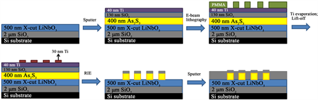
Figure 6. Fabrication of the basic grating coupler structure (side view).
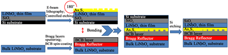
Figure 7. Proposed fabrication flow of the improved structure (side view).

Figure 8. Insertion loss of the basic grating couplers with an As2S3 waveguide.
Table 3. Comparison between two grating couplers.
coupler and the waveguide, there is a 200 μm long linear taper, with the wider tip of 12 μm connecting the grating coupler and the narrower tip of 1 μm connecting the waveguide. The grating coupler period is 0.85 μm. Due to the fabrication imperfection, the peak transmission wavelength is shifted to the shorter wavelength range. As a rough estimation, the propagation loss at 1540 nm is 2.0 dB/cm. Assuming that the mode conversion loss in both tapers is negligible and the waveguide loss is wavelength-independent, the lowest fabricated grating coupler loss is 6.3 dB at 1540 nm. Compared to the experimental result in [11] , the grating coupler efficiency in this work is 2.55 dB worse, due to the fact that there is no Bragg reflector in this basic grating coupler structure, and the light is partially leaked through substrate.
The difference between measured grating coupler loss and simulation result is due to several factors: first, the overall insertion loss includes the SMF tails that are used to couple the OVA source/detector to the grating couplers. Since it is not convenient to isolate the fiber tails from the device under test (DUT), the surface qualities of those fiber tails and light propagation loss inside them would result in higher calculated grating coupler loss. Similarly, the tapers’ loss might also be one contributing factor to the overall loss. In terms of fabrication, surface roughness caused by topology of the grating coupler can also result in lower coupling efficiency than theoretical prediction. During measurement, any small angular offset of the sample orientation would cause additional loss.
In order to improve the grating coupler performance, the grating period and DC need to be tweaked from the design values based on the current experimental results, since the actually materials and their refractive indices are off from the material database to some extent. Longer taper could be included in order to further reduce mode-conversion loss.
The basic grating coupler can be used to measure As2S3 grating cavity structure on thin film LiNbO3. With electrode patterned on both sides of the cavity waveguide, it becomes EO tunable filters. Grating cavity reflection response can be extracted by truncation of the time domain impulse reflection (including grating coupler), followed by inverse Fourier transformation. Figure 9(a) shows the whole device, highlighting the grating cavity section in dashed box. Figure 9(b) shows the reflected spectrum of one fabricated Fabry-Perot (FP) cavity extracted in this manner. This device is constructed by 1000 periods of sidewall Bragg gratings, with period of 360 nm and grating depth of 200 nm. The cavity length is 3 mm and the cavity width is 1 µm. The fitted result in Figure 9(c) is calculated by implementing coupled-mode theory (CMT) and transfer matrix method (TMM) with the fitting parameters listed in Table 4.
Optical confinement factor in LiNbO3 layer is a key parameter for EO tuning applications. Higher confinement factor in LiNbO3 layer means more effective EO tuning, since LiNbO3 crystal is the only EO tunable material in this structure. By decreasing As2S3 waveguide width, confinement factor in thin film LiNbO3 can be effectively increased, as shown in Figure 10. 500 nm X-cut LiNbO3 on top of 2 μm SiO2 on a Si wafer is used in the simulation. With 0.4 µm waveguide width, the confinement factor is 82.3%.
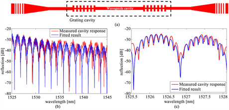
Figure 9. (a) Grating cavity device under test. The dashed box is the grating cavity section; (b) Reflection spectrum of a fabricated grating cavity device; (c) Zoom-in reflection.

Figure 10. Effective refractive index of the hybrid and optical confinement factor in thin film LiNbO3 change with different As2S3 waveguide widths.
Table 4. Fitting parameters for the grating cavity reflection response.
5. Conclusions
As2S3 grating coupler on thin film LiNbO3 is designed in order to open the door to multiple EO applications with thin film LiNbO3. A basic grating coupler structure is fabricated and the experimental results show 23.4% coupling efficiency while the simulation is at 53.0%. The efficiency difference is due to fabrication imperfection, testing fibers, and misalignment during measurement. An improved grating coupler is designed, and the theoretical coupling efficiency can be as high as 78.8% at 1550 nm with 60 nm bandwidth.
As2S3 waveguide propagation loss of 2.0 dB/cm is calculated through TMM fitting a grating cavity measurement result enabled by the As2S3 grating coupler. A simulation of As2S3 waveguide cross-section on a 500 nm thin film LiNbO3 result indicates as high as 82.3% optical confinement in LiNbO3 layer if the As2S3 cavity waveguide width is reduced to 0.4 μm. This means that high EO tuning efficiency can be achieved on thin film LiNbO3 layer, once an electric field is properly applied across the cavity waveguide section.
Acknowledgements
The authors would thank Dr. Long Chang from The University of Houston Nanofabrication Facility for valuable discussion on E-beam lithography.
Cite this paper
Zhang, C. and Madsen, C.K. (2018) Demonstration of an As2S3 Grating Coupler on Thin Film LiNbO3. Optics and Photonics Journal, 8, 111-121. https://doi.org/10.4236/opj.2018.84011
References
- 1. Snider, W.T., Macik, D.D. and Madsen, C.K. (2012) Electro-optically Tunable Mach-Zehnder Interferometer on LiNbO3 Substrate. IEEE Photonics Technology Letters, 24, 1415-1417. https://doi.org/10.1109/LPT.2012.2205377
- 2. Macik, D.D. and Madsen, C.K. (2016) Fabrication of LiNbO3-As2S3 Waveguides for Beam Steering Applications. Proceedings of SPIE, San Diego, 14 September 2016, Article ID: 99700H-10.
- 3. Wooten, E.L., Kissa, K.M., Yi-Yan, A., Murphy, E.J., Lafaw, D.A., Hallemeier, P.F., Maack, D., Attanasio, D.V., Fritz, D.J., McBrien, G.J. and Bossi, D.E. (2000) A Review of lithium Niobate Modulators for Fiber-Optic Communications Systems. IEEE Journal of Selected Topics in Quantum Electronics, 6, 69-82. https://doi.org/10.1109/2944.826874
- 4. Rao, A., et al. (2015) Heterogeneous Microring and Mach-Zehnder Modulators Based on Lithium Niobate and Chalcogenide Glasses on Silicon. Optics Express, 23, 22746-22752. https://doi.org/10.1364/OE.23.022746
- 5. Guarino, A., Poberaj, G., Rezzonico, D., Degl’Innocenti, R. and Günter, P. (2007) Electro-Optically Tunable Microring Resonators in Lithium Niobate. Nature Photonics, 1, 407-410. https://doi.org/10.1038/nphoton.2007.93
- 6. Levy, M., Osgood, R., Liu, R., Cross, L., Cargill, G., Kumar, A., et al. (1998) Fabrication of Single-Crystal Lithium Niobate Films by Crystal Ion Slicing. Applied Physics Letters, 73.
- 7. Ramadan, T.A., Levy, M. and Osgood, R. (2000) Electro-Optic Modulation in Crystal-Ion-Sliced z-Cut LiNbO3 Thin Films. Applied Physics Letters, 76, 1407. https://doi.org/10.1063/1.126046
- 8. Lu, H., Sadani, B., Courjal, N., Ulliac, G., Smith, N., Stenger, V., et al. (2012) Enhanced Electro-Optical Lithium Niobate Photonic Crystal Wire Waveguide on a Smart-Cut Thin Film. Optics Express, 20, 2974-2981. https://doi.org/10.1364/OE.20.002974
- 9. Wang, X., Zhou, Y. and Madsen, C.K. (2014) Fabrication and Measurement of Sidewall Gratings Integrated in Hybrid As2S3-Ti:LiNbO3 Optical Waveguides. Journal of Lightwave Technology, 32, 2989-2995. https://doi.org/10.1109/JLT.2014.2334054
- 10. Zhou, Y., Wang, X., Zhang, C. and Madsen, C.K. (2015) Resonant Enhanced Low-Power Nonlinear Tuning Capability Using an As2S3 Waveguide on LiNbO3. Proceedings of SPIE, San Francisco, 2 April 2015, 936514.
- 11. Zhang, C. and Madsen, C.K. (2016) Demonstration of an As2S3-on-LiNbO3 Grating Coupler and Its Application of Measuring a Grating-Based Filter. IEEE Photonics Journal, 8, 1-7. https://doi.org/10.1109/JPHOT.2016.2616220
- 12. Polyanskiy, M.N. (2017) Refractive Index Database. https://refractiveindex.info
- 13. Dakss, M.L., Kuhn, L., Heidrich, P.F. and Scott, B.A. (1970) Grating Coupler for Efficient Excitation of Optical Guided Waves in Thin Films. Applied Physics Letters, 16, 523-525. https://doi.org/10.1063/1.1653091
- 14. Niklaus, F., Enoksson, P., Kälvesten, E. and Stemme, G. (2001) Low-Temperature Full Wafer Adhesive Bonding. Journal of Micromechanics and Microengineering, 11, 100. https://doi.org/10.1088/0960-1317/11/2/303
- 15. Niklaus, F., Andersson, H., Enoksson, P. and Stemme, G. (2001) Low Temperature Full Wafer Adhesive Bonding of Structured Wafers. Sensors and Actuators A: Physical, 92, 235-241. https://doi.org/10.1016/S0924-4247(01)00568-4
- 16. Processing Procedures for BCB Adhesion. DOW. http://www.dow.com/cyclotene/docs/bcb_adhesion.pdf