Optics and Photonics Journal
Vol.3 No.8A(2013), Article ID:41427,5 pages DOI:10.4236/opj.2013.38A004
Influence of Thickness and Annealing Temperature on the Optical Properties of Spin-Coated Photoactive P3HT:PCBM Blend
1Department of Applied Physics & Electronic Engineering, Rajshahi University, Rajshahi, Bangladesh
2Department of Material Science & Engineering, Rajshahi University, Rajshahi, Bangladesh
3Department of Analog & Optoelectronics, Cologne University of Applied Sciences, Cologne, Germany
Email: *ismail@ru.ac.bd
Copyright © 2013 Md. Shahinul Islam et al. This is an open access article distributed under the Creative Commons Attribution License, which permits unrestricted use, distribution, and reproduction in any medium, provided the original work is properly cited.
Received July 9, 2013; revised August 13, 2013; accepted September 11, 2013
Keywords: Organic Semiconductor; Photoactive Polymer; Bulk Heterojunction; Solar Energy Materials
ABSTRACT
Influence of annealing temperature and thickness on the optical characteristics of the blend of poly (3-hexylthiophene) (P3HT) and Phenyl C61 butyric acid methylester (PCBM) layer has been investigated in this report. Photoactive polymer material (P3HT:PCBM) was deposited on indium tin oxide (ITO) substrate by spin-coating. The morphology of P3HT:PCBM composite layer was investigated by Atomic Force Microscope (AFM). The surface roughness was found to reduce after heat treatment. The absorption of the composite layer was found to increase with its number of layer (thickness). On the other hand, the photoluminescence (PL) quenching, which indicates efficient charge separation in the bulk heterojunction, was found higher for the thinner layer. Absorption was also found to increase with the annealing temperature. Therefore, to optimize the thickness of the P3HT:PCBM photoactive layer that will provide best absorption while providing efficient charge separation, annealing at optimized temperature might be an effective tool.
1. Introduction
Recently superb performance has been demonstrated from the bulk heterojunction photovoltaic devices using P3HT as donor and PCBM as acceptor [1-3]. P3HT and PCBM have several advantages such as low-cost fabrication, large-area devices, lightweight cells with flexibility, and material diversity [4,5]. In a blend, the performance of P3HT and PCBM as a thin-film heterojunction depends on various parameters, such as film growth methods [6], processing conditions [7], morphology of the deposited thin-film [8], heat treatment [9] etc. It has useful optoelectronic properties such as, a good chemical stability, high mobility, and low optical band gap [10,11]. Especially, with higher hole-mobility of 0.1 cm2/V.s, P3HT offers the possibility of realizing high-efficiency BHJ PV cells [12,13]. P3HT:PCBM-based device performance is highly influenced by the molecular weight of P3HT, the dissolving solvent, and thermal annealing [14-16], and researchers have focused on the optical/morphological properties of P3HT:PCBM films. Based on the above background in this report, the change in optical properties of the blend of P3HT:PCBM with film layer thickness and annealing has been studied. We found that the annealing temperature might be an effective tool for optimizing the thickness of the P3HT:PCBM layer that might provide best absorption and efficient charge separation.
2. Experimental
Readymade blend of P3HT and PCBM at 1:1 ratio was bought from Sigma-Aldrich, Germany, and was used without further purification. ITO thin films were deposited on a glass substrate at room temperature by electron beam evaporation technique. The commercially available ITO powder (99.99% pure) obtained from Inframat Advanced Materials, USA, and was used as the evaporation source material. The ITO films were annealed at 600˚C in air to obtain a transparency of 90%. The blend of P3HT:PCBM was warmed at 45˚C for 20 minutes to make it homogenous prior to spin coating. This blend was then deposited by spin coating on ITO at speed of 200 rpm in air. After deposition whole structure was annealed in air at 130˚C for 2 minutes.
3. Results and Discussion
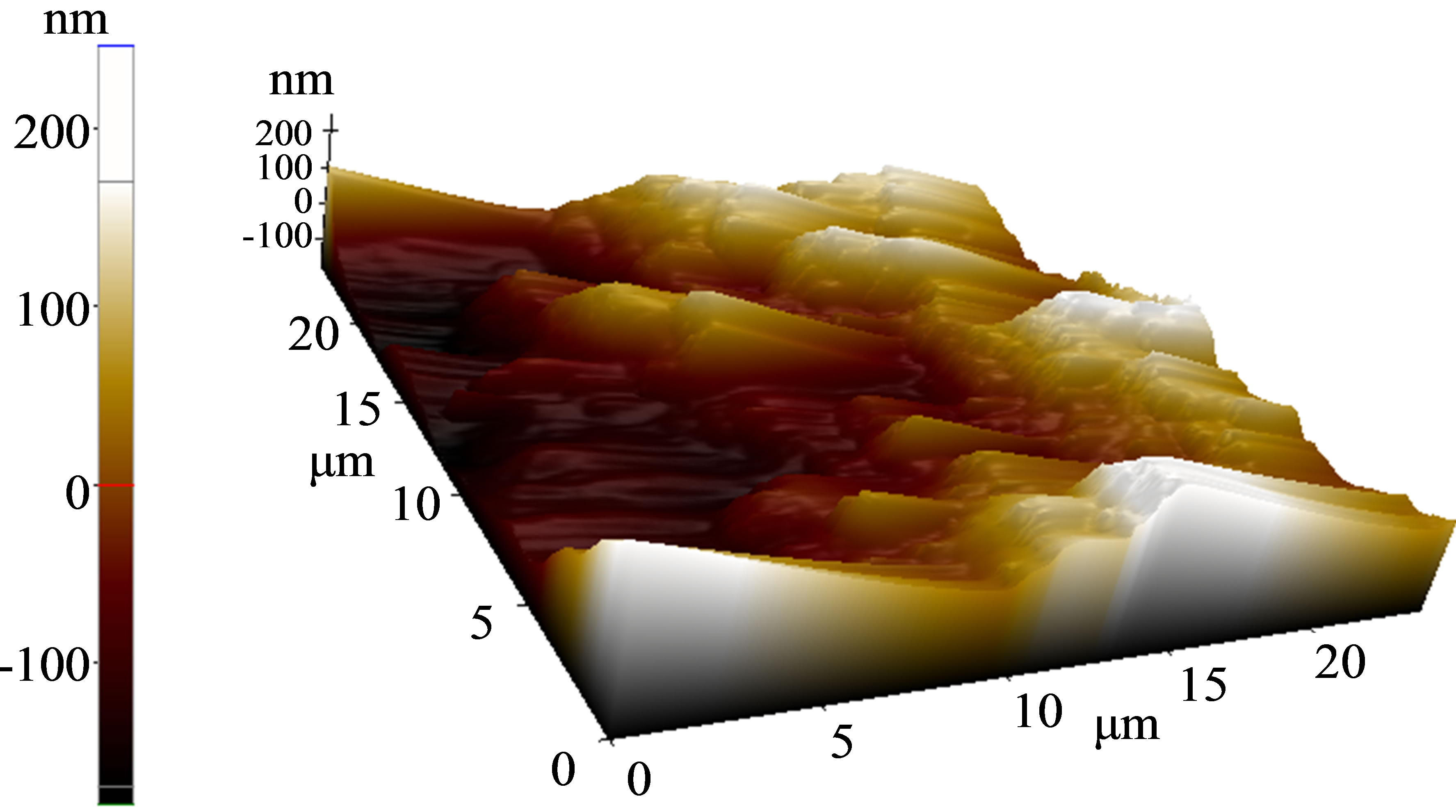
The surface morphology of as-deposited and annealed P3HT:PCBM composite layer was studied by AFM. The rough surface represents the self-organization of P3HT that also indicate ordered structure formation in the thin film [17]. But it can also lead to poor contact with the electrode. The roughness of our as-deposited layer (0.5 nm) reduced significantly (0.04 nm) after annealing as evident from Figure 1.
The absorption characteristics of P3HT:PCBM composite film was investigated in the wavelength 300 - 700 nm. The P3HT:PCBM film showed a significant change in absorption when the layer thickness was increased. From Figure 2 we observe that absorption increased with the increasing layer thickness. For the as spun films all the films with various thicknesses showed a main peak around 510 nm. But when the layer thickness was increased to 3-layers (~150 nm) a shoulder peak appeared around 445 nm. This peak is believed to originate from the highly crystalline P3HT domains with improved stacking [17,18].
Figure 3 shows the optical absorption spectra after heat treatment (annealing) for single layer of P3HT:
 (a)
(a)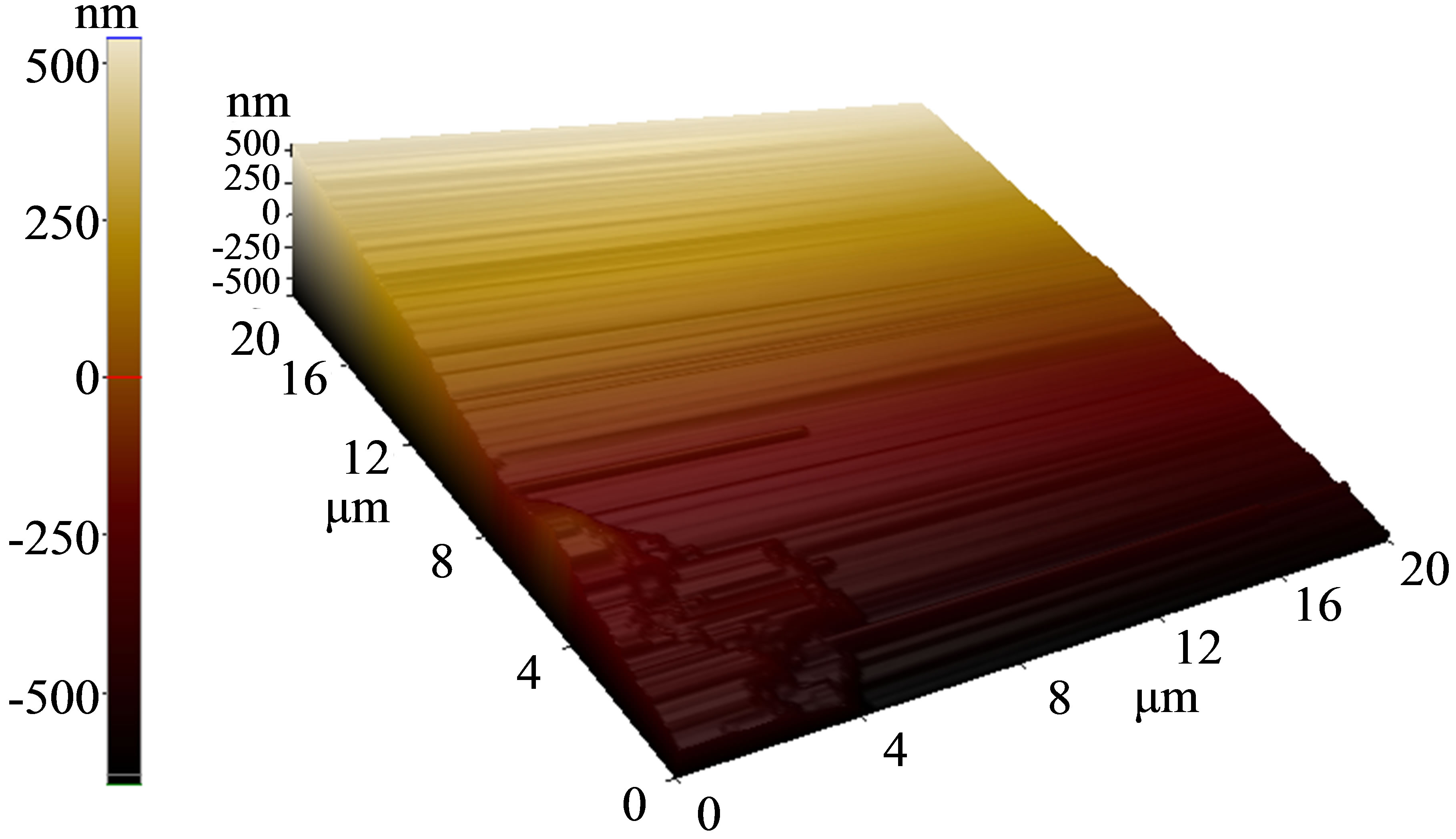 (b)
(b)
Figure 1. (a) As-deposited surface morphology of photoactive layer; (b) P3HT:PCBM surface after heat treatment.
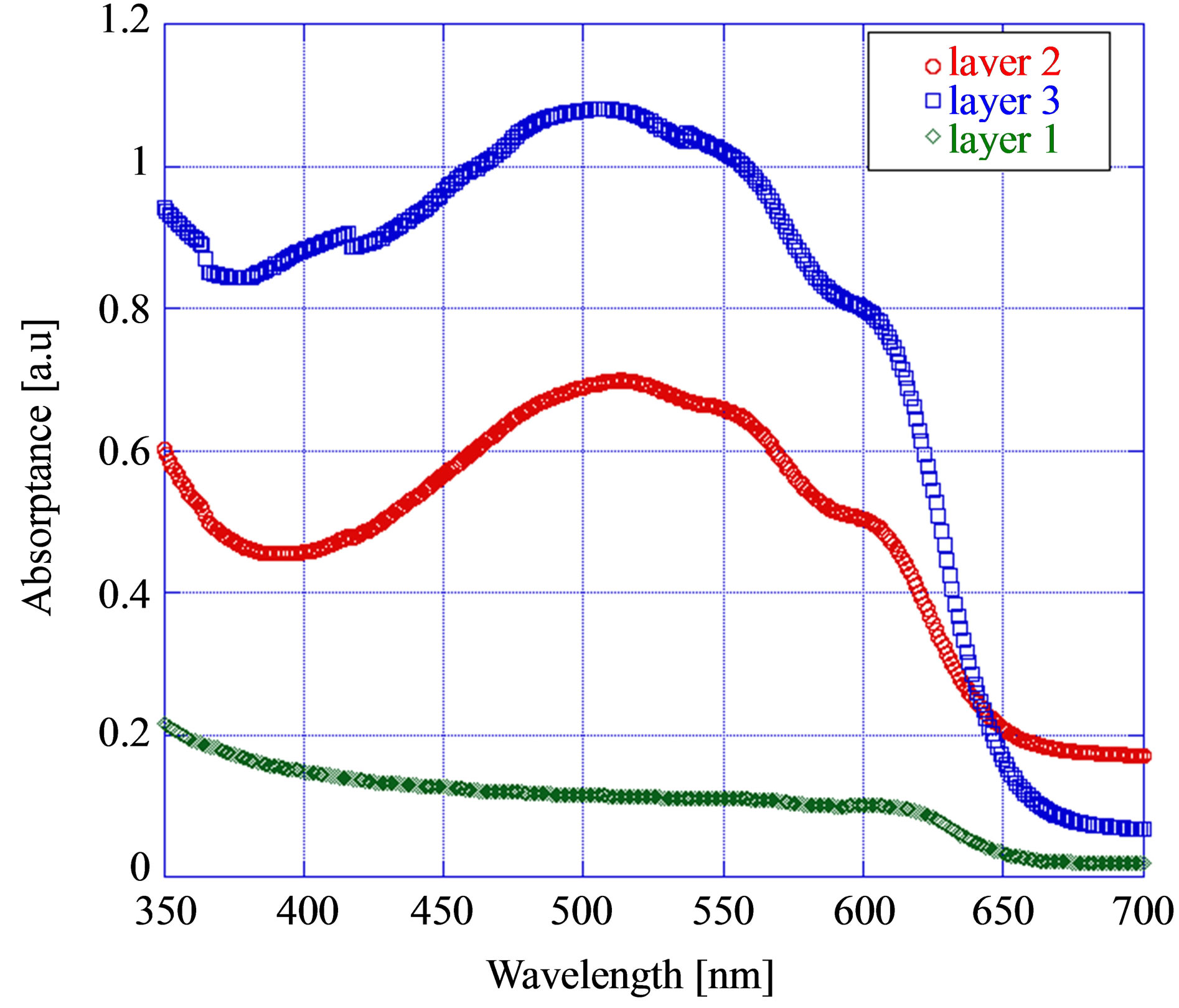
Figure 2. Variation of absorption of photoactive layer with the layer thickness.
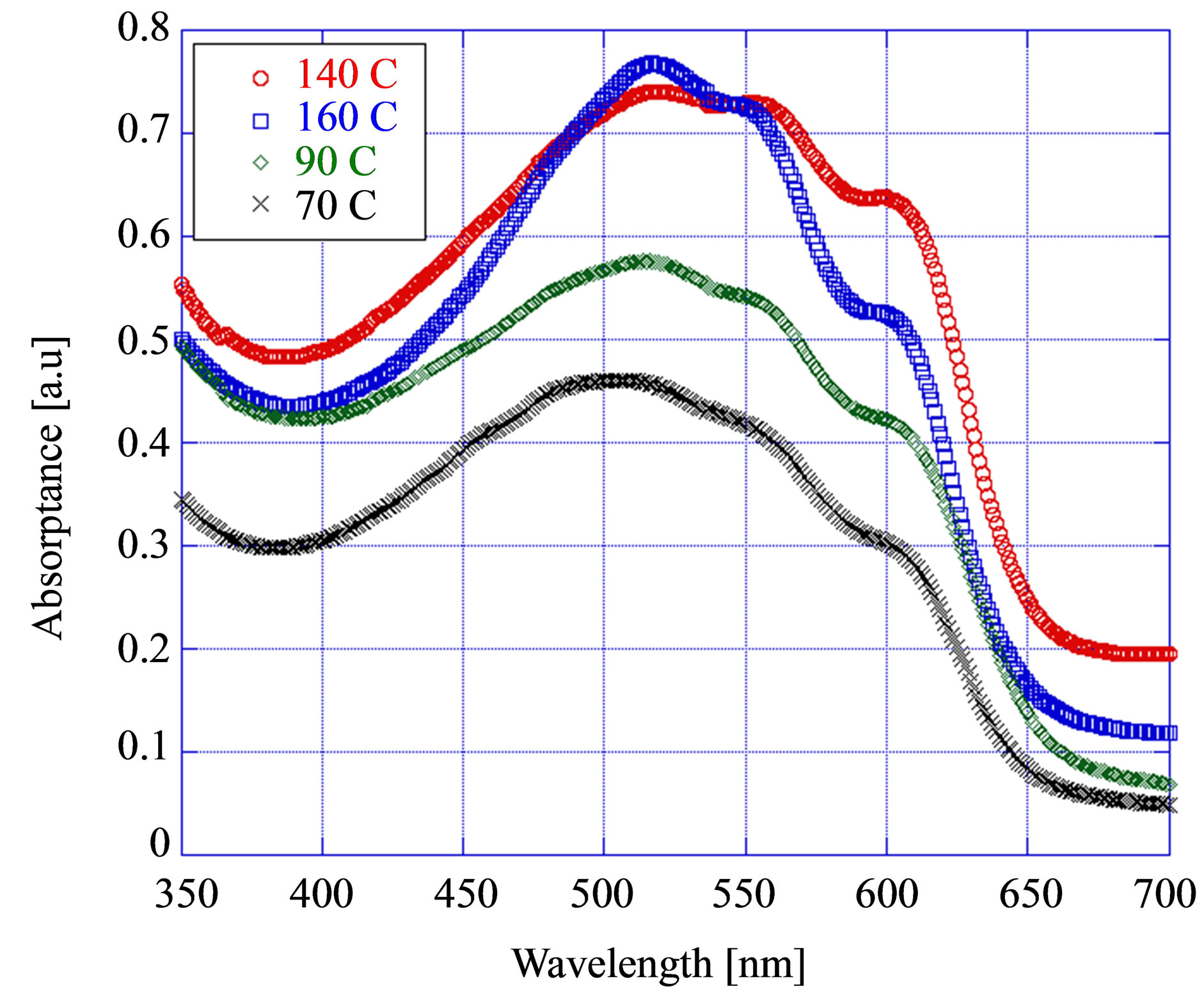
Figure 3. Variation of absorption with annealing temperature.
PCBM. It is interesting to note that the absorbance of the film increased and red-shifted gradually with the thermal annealing process and the largest increase was found for the annealing at the high temperature of 140˚C. The annealing enhances the crystallinity of P3HT caused by the diffusion of PCBM molecules into aggregates causing the P3HT molecules to be crystallized in the free region of PCBM that leads to more π-π* absorption. As a result highest crystallinity and maximum absorption were observed at an annealing temperature of 140˚C. Generally the absorption peak band signifies the π-π* transition of the P3HT backbone [19]. This increased absorption after annealing is believed to be due to chain ordering of P3HT domains induced by heat treatment, the development of bigger aggregates or, more condensed moieties which are composed of multiple inter-chain species of P3HT, packing of the P3HT domains, and reduced torsion of the P3HT.
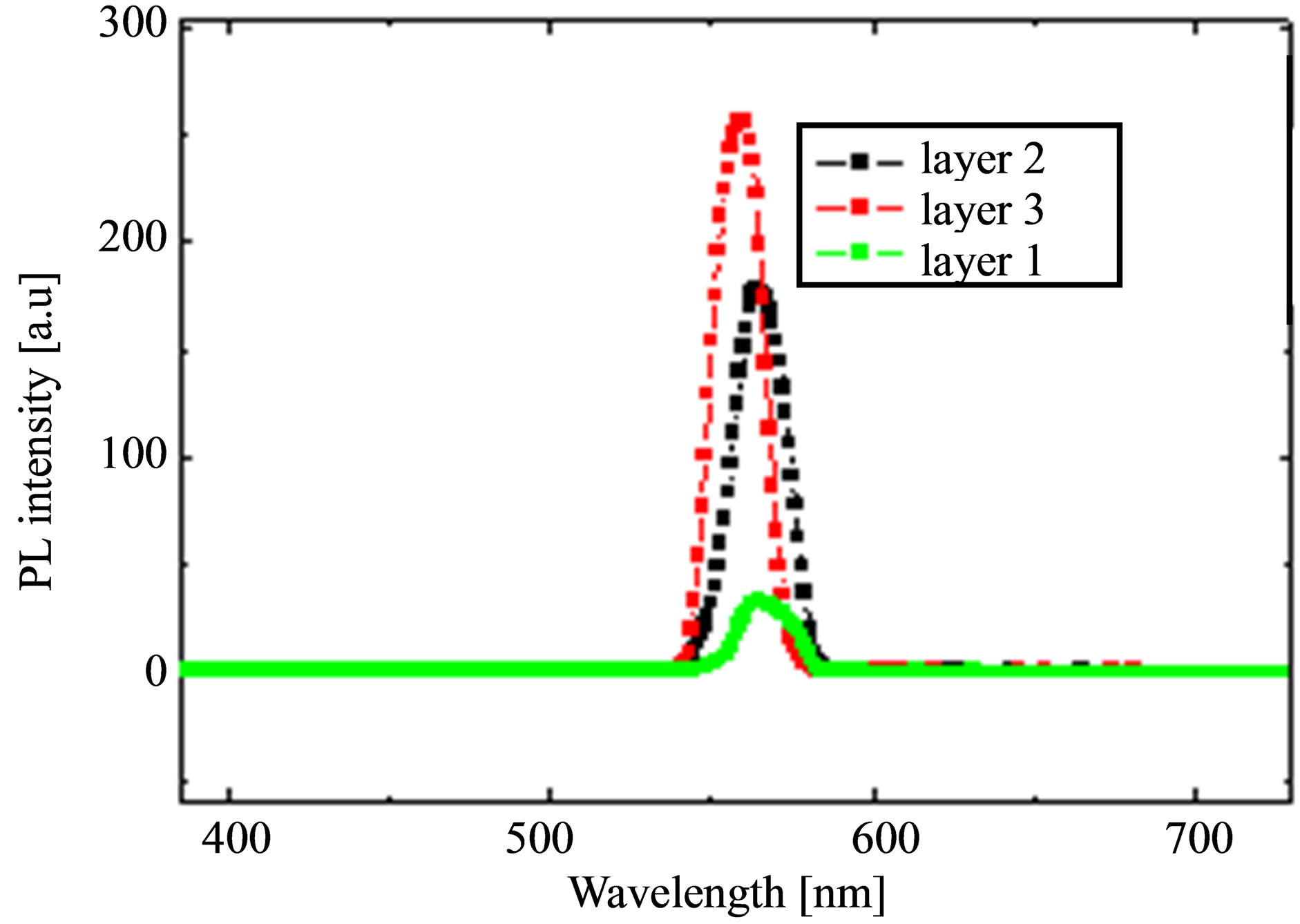
Photoluminescence (PL) spectra of P3HT:PCBM for various layer-thickness is shown in Figure 4, from which we observed that there is photoluminescence quenching depends on the thickness. PL quenching increased with thinner layer that indicates existence of well-mixed states of electron donors (P3HT) and acceptors (PCBM) that in turn facilitates rapid transfer charges [20]. When, layer thickness of P3HT:PCBM reaches 3-layers photons are more absorbed by P3HT:PCBM and less photons is converted into charge carrier collection because layer thickness became much longer than the exciton diffusion length. As the film thickness reaches 3-layers, essentially incident light between 350 and 610 nm is absorbed in one optical path. This spectral response indicates that photons that are more strongly absorbed by P3HT are less likely to be converted into collected charge carriers, as observed in planar heterojunction devices with a layer thickness much greater than exciton diffusion length [21].
 (a)
(a)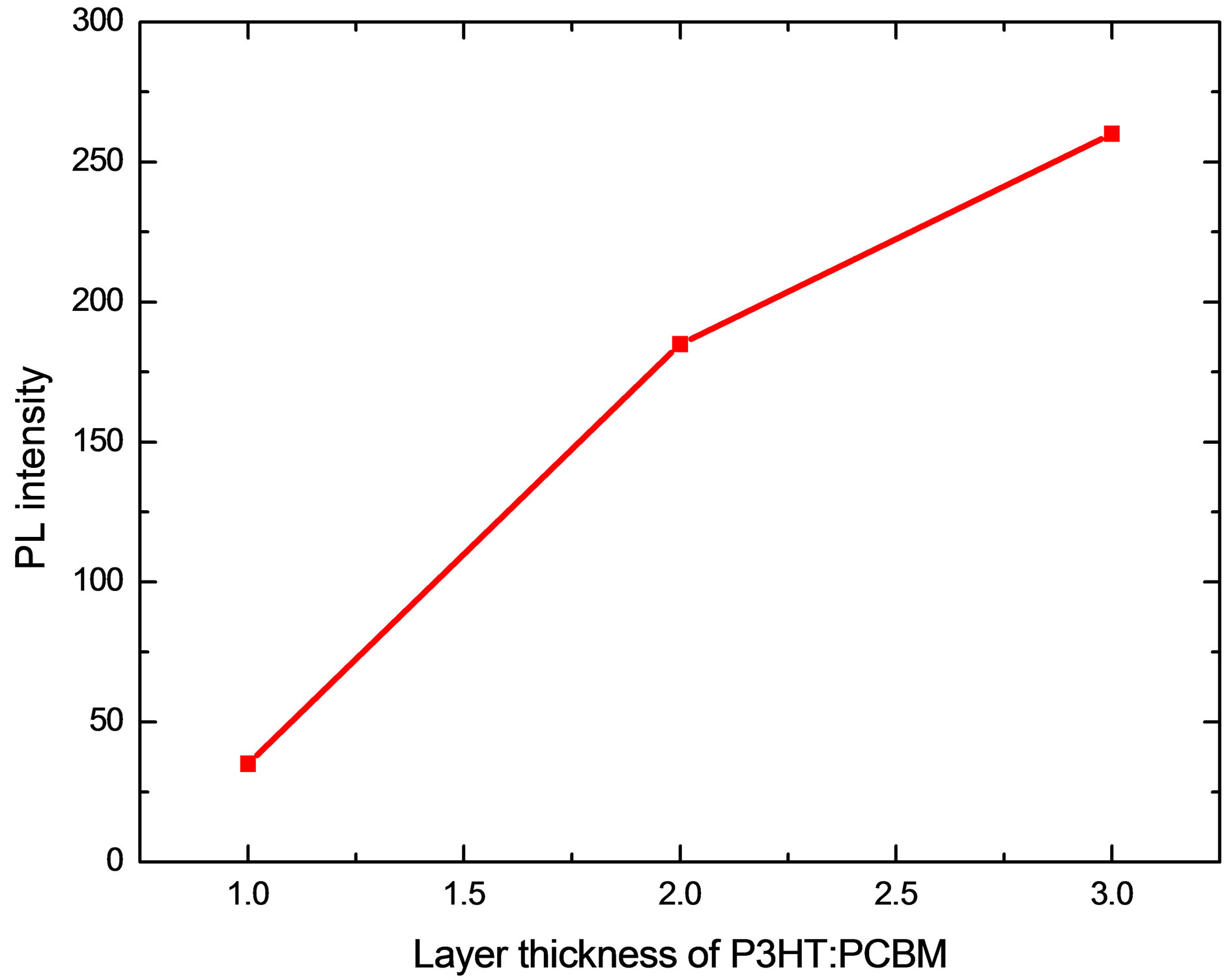 (b)
(b)
Figure 4. (a) Photoluminescence (PL) spectra for layers of various thicknesses and (b) PL quenching.
Photons with wavelength in the weakly absorbing region can penetrate deeper into the active layer where more abundant P3HT:PCBM interfaces are available for efficient exciton dissociation.
The absorbance of light by a sample depends on the concentration of absorbers, the path length of the light through the sample, and the extinction coefficient. Figure 5 shows the plot of extinction coefficient versus annealing temperature. The extinction coefficient has been calculated assuming a typical absorption length (Optical Path length) of conjugated polymers (α−1 = 100 nm) and concentration of 2.2% of P3HT:PCBM blend [22]. The value of extinction coefficient was found to increase with annealing temperature in the range between 400 - 500 nm. A high value of extinction coefficient means in the absorption band is caused by crystallization of the polymer material leading to more π-π* absorption. It appears from the above discussion that annealing could be an efficient method for controlling the optical properties of the film that in tern could be used to optimize layer thickness.
4. Conclusion
Spin-coated organic photoactive polymer material (P3HT: PCBM blend) has been investigated for the optimization of active layer thickness foreseeing its application in organic photovoltaics. The surface roughness obtained from the AFM of P3HT:PCBM layer indicated a very smooth coating of the photoactive layer on ITO. The influence of P3HT:PCBM layer thickness and annealing temperature on the absorption characteristic has been investigated. It was observed that the absorption increased with the increase in layer thickness and annealing temperature. Similar results were report by Moule [23] and Kim [24].

Figure 5. Variation of extinction coefficient with annealing temperature.
But the photoluminescence (PL) quenching was higher than the thinner layer, which is essential for a bulk heterojunction. As a compromise, annealing temperature can be used to optimize the absorption and charge separation of P3HT:PCBM heterojunction to be used in organic photovoltaics. Therefore spin-coated single layer of P3HT:PCBM layer annealed at 140˚C might provide the required absorption and efficient charge separation for the organic polymer blend to be used as a bulk heterojunction.
REFERENCES
- P. Schilinsky, C. Waldauf and C. J. Brabec, “Recombination and Loss Analysis in Polythiophene Based Bulk Heterojunction Photodetectors,” Applied Physics Letters, Vol. 81, No. 20, 2002, p. 3885. http://dx.doi.org/10.1063/1.1521244
- F. Padinger, R. S. Rittberger and N. S. Sariciftci, “Effects of Postproduction Treatment on Plastic Solar Cells,” Advanced Functional Materials, Vol. 13, No. 1, 2003, pp. 85-88. http://dx.doi.org/10.1002/adfm.200390011
- D. Chirvase, J. Parisi, J. C. Hummelen and V. Dyakonov, “Influence of Nanomorphology on the Photovoltaic Action of Polymer-Fullerene Composites,” Nanotechnology, Vol. 15, No. 9, 2004, p. 1317. http://dx.doi.org/10.1088/0957-4484/15/9/035
- H. Sirringhaus, et al., “Two-Dimensional Charge Transport in Self-Organized, High-Mobility Conjugated Polymers,” Nature, Vol. 401, 1999, pp. 685-688. http://dx.doi.org/10.1038/44359
- J. Y. Seong, et al., “Variational, Method for the Lowest Conduction Subband of Undoped AlGaN/GaN Single Heterojunctions,” Journal of the Korean Physical Society, Vol. 45, 2004, p. 5914.
- J. P. Zhou, X. H. Chen and Z. Xu, “Influence of P3HT: PCBM Film Formation Process on the Performance of Polymer Solar Cells,” Spectroscopy and Spectral Analysis, Vol. 31, No. 10, 2011, pp. 2684-2687
- A. Ng, Y. C. Sun, M. K. Fung, A. M. C. Ng, Y. H. Leung, A. B. Djurišić and W. K. Chan, “Influence of the Polymer Processing Conditions on the Performance of Bulk Heterojunction Solar Cells,” SPIE Proceedings, Organic Photonic Materials and Devices XIV, Vol. 8258, 2012, 82581E. http://dx.doi.org/10.1117/12.907660
- V. S. Balderrama, et al., “Influence and Relationship of Film Morphology on Organic Solar Cells Manufactured with Different P3HT:PC[70]BM Blend Solutions,” 8th International Conference on Electrical Engineering Computing Science and Automatic Control, Vol. 1, No. 5, 2011, pp. 26-28.
- P. Kumer, et al., “Effect of Thermal Treatment on the Performance of Organic Bulk-Hetrojunction Photovoltaic Devices, Physics of Semiconductor Devices,” International Workshop on IWPSD, Mumbai, 16-20 December 2007, pp. 16-20.
- W. R. Salaneck, et al., “Thermochromism in Poly(3-Hexylthiophene) in the Solid State: A Spectroscopic Study of Temperature-Dependent Conformational Defects,” Journal of Chemical Physics, Vol. 89, No. 8, 1988, p. 4613. http://dx.doi.org/10.1063/1.454802
- Y. Zhao, G. Yuan, P. Reche and M. Lecerc, “A Calorimetric Study of the Phase Transitions in Poly(3-Hexylthiophene),” Polymer, Vol. 36, No. 11, 1995, pp. 2211- 2214. http://dx.doi.org/10.1016/0032-3861(95)95298-F
- P. J. Brown, H. Sirringhaus, M. Harrison, M. Shkunov and R. H. Friend, “Optical Spectroscopy of Field-Induced Charge in Self-Organized High Mobility Poly(3-Hexylthiophene),” Physical Review B, Vol. 63, No. 12, 2001, Article ID: 125204. http://dx.doi.org/10.1103/PhysRevB.63.125204
- X. Yang, et al., “Nanoscale Morphology of High-Performance Polymer Solar Cells,” Nano Letters, Vol. 5, No. 4, 2005, pp. 579-583. http://dx.doi.org/10.1021/nl048120i
- A. Zen, et al., “Effect of Molecular Weight and Annealing of Poly(3-Hexylthiophene)s on the Performance of Organic Field-Effect Transistors,” Advanced Functional Materials, Vol. 14, No. 8, 2004, pp. 757-764. http://dx.doi.org/10.1002/adfm.200400017
- M. Al-Ibrahim, O. Ambacher, S. Sensfuss and G. Gobsch, “Effects of Solvent and Annealing on the Improved Performance of Solar Cells Based on Poly(3-Hexylthiophene): Fullerene,” Applied Physics Letters, Vol. 86, No. 20, 2005, Article ID: 201120. http://dx.doi.org/10.1063/1.1929875
- Y. Kim, et al., “Device Annealing Effect in Organic Solar Cells with Blends of Regioregular Poly(3-Hexylthiophene) and Soluble Fullerene,” Applied Physics Letters, Vol. 86, No. 6, 2005, Article ID: 063502. http://dx.doi.org/10.1063/1.1861123
- G. Li, et al., “High-Efficiency Solution Processable Polymer Photovoltaic Cells by Self-Organization of Polymer Blends,” Nature Materials, Vol. 4, 2005, pp. 864-868. http://dx.doi.org/10.1038/nmat1500
- W. L. Ma, C. Y. Yang, X. Gong, K. Lee and A. J. Heeger, “Thermally Stable, Efficient Polymer Solar Cells with Nanoscale Control of the Interpenetrating Network Morphology,” Advanced Functional Materials, Vol. 15, No. 10, 2005, pp. 1617-1622. http://dx.doi.org/10.1002/adfm.200500211
- H. Sirringhaus, et al., Two-Dimensional Charge Transport in Self-Organized, High-Mobility Conjugated Polymers,” Nature, Vol. 401, 1999, pp. 685-688. http://dx.doi.org/10.1038/44359
- B. K. Kuila and A. K. Nandi, “Physical, Mechanical, and Conductivity Properties of Poly(3-hexylthiophene)-Montmorillonite Clay Nanocomposites Produced by the Solvent Casting Method,” Macromolecules, Vol. 37, No. 23, 2004, pp. 8577-8584. http://dx.doi.org/10.1021/ma0490496
- M. Drees, R. M. Davis and J. R. Heflin, “Thickness Dependence, in Situ Measurements, and Morphology of Themally-Controlled Interdiffusion in Polymer-C60 Photovoltaic Devices,” Physical Review B, Vol. 69, No. 16, 2004, Article ID: 165320. http://dx.doi.org/10.1103/PhysRevB.69.165320
- H. Ohkita and S. Ito, “Transient Absorption Spectroscopy of Polymer-Based Thin-Film Solar Cells,” Polymer, Vol. 52, No. 20, 2011, pp. 4397-4417. http://dx.doi.org/10.1016/j.polymer.2011.06.061
- A. J. Moule, et al., “The Effect of Active Layer Thickness and Composition on the Performance of Bulk-Heterojunction Solar Cells,” Journal of Applied Physics, Vol. 100, No. 9, 2006, Article ID: 094503. http://dx.doi.org/10.1063/1.2360780
- H. Kim, W.-W. So and S.-J. Moon, “Effect of Thermal Annealing on the Performance of P3HT/PCBM Polymer Photovoltaic Cells,” Journal of the Korean Physical Society, Vol. 48, 2006, pp. 441-445.
NOTES
*Corresponding author.