Journal of Surface Engineered Materials and Advanced Technology
Vol.3 No.3(2013), Article ID:34219,6 pages DOI:10.4236/jsemat.2013.33024
Improved Photovoltaic Properties of Heterojunction Carbon Based Solar Cell
![]()
1Department of Electronics and Information Engineering, Chubu University, Kasugai, Japan; 2Department of Hydrology and Meteorology, Tri-Chandra Campus, Tribhuvan University, Kathmandu, Nepal; 3Shinko Seiki Co., Ltd., Kobe, Japan.
Email: *sudip@isc.chubu.ac.jp
Copyright © 2013 Sudip Adhikari et al. This is an open access article distributed under the Creative Commons Attribution License, which permits unrestricted use, distribution, and reproduction in any medium, provided the original work is properly cited.
Received April 6th, 2013; revised May 7th, 2013; accepted June 1st, 2013
Keywords: Carbon; Photovoltaic Properties; Heterojunction Solar Cell
ABSTRACT
Amorphous carbon (a-C) thin films have been synthesized by microwave (MW) surface wave plasma (SWP) chemical vapor deposition (CVD) on n-type silicon and quartz substrates, aiming at the application of the films for photovoltaic solar cells. Argon, acetylene and trimethylboron were used as a carrier, source and dopant gases. Analytical methods such as X-ray photoelectron spectroscopy (XPS), Hall Effect measurement, JASCO V-570 UV/VIS/NIR spectroscopy, Raman spectroscopy, Transmission electron microscopy (TEM) and Solar simulator were employed to investigate chemical, optical, structural and electrical properties of the a-C films. Two types of solar cells of configuration p-C/n-Si and p-C/i-C/n-Si have been fabricated and their current-voltage characteristics under dark and illumination (AM 1.5, 100 mW/cm2) have been studied. The two solar cells showed rectifying curves under the dark condition confirming the heterojunction carbon based solar cell between p-C and n-Si. When illuminated by the solar simulator light the devices showed photovoltaic behavior. The heterojunction device (p-C/i-C/n-Si) having inserted intrinsic carbon film between p-C and n-Si exhibited significant enhancement of the conversation efficiency (0.167% to 2.349%) over the device (p-C/n-Si).
1. Introduction
Various semiconductor materials have been used to fabricate solar cells that convert sunlight into electricity. Among them, silicon based solar cells are dominant in the market which are expensive, and thus not practical to use for daily life. Also, release of a toxic gas (SiO2) while fabricating silicon based solar cells is discouraging for environment and consequently to human health. Therefore, the cost reduction of solar cell and establishment of environmentally friendly production process are very important for development and promotion of photovoltaic technology in the near future. One of the attractive alternatives is the application of carbon based solar cell that can be fabricated from cheap, abundant and nontoxic precursors [1,2]. Carbon an element of group IV in the periodic table existing in many forms with a wide range of optoelectronic properties has been found as a highly attractive material for its possible application in Photovoltaic (PV) solar cells [3]. It consists of a mixture of trihedral (sp2) and tetrahedral (sp3) configurations and hence possible to vary the optical band gap by simply varying the relative proportion of the sp2/ sp3 hybridization [4].
Amorphous carbon (a-C) films have received considerable attention because of their unique properties such as extreme hardness and chemical inertness. Interestingly, these properties can be tailored over a wide range, which promotes its application in the semiconductor field [5,6]. These properties are attractive for optoelectronics device including photovoltaic solar cells. Optoelectronics properties of the a-C thin films strongly depend on the deposition method and other parameters. Generally, two methods; physical deposition or sputtering method and chemical vapor deposition (CVD) are used for synthesis of a-C films. The sputtering methods, such as ion beam sputtering [7,8], magnetron sputtering [9] and pulse laser deposition [8,10,11] usually use solid target, and the CVD methods, such as radio frequency (RF) plasma CVD [12-14] and plasma-enhanced CVD [15,16] involve the decomposition of hydrocarbon source gas (C2H2, C2H4, CH4 etc). The gaseous phase of carbon source used in CVD has the advantage of better control of chemical composition and bonding structure in the thin films over the solid source used in the physical deposition method. The a-C films were synthesized by various methods, and properties of the films were extensively studied for various applications. Some of the previous works were purely concentrated to develop a-C thin film based heterojunction solar cells [1,3,7-20].
The application of a-C on the semiconductor field was the subject of many investigations [21,22]. However, undoped a-C is weakly p-type [23] in nature, and the complex structure and presence of high density of defects restrict its ability to dope efficiently and are the main barrier for its application in various electronic devices, such as PV cells. When attempted to utilize such carbon as an alternative material in PV cells, control of optical band gap and conduction type through doping of carbon film are indispensable. The doping mechanism of amorphous semiconductors has always been an interesting issue. The semiconducting carbon films can be either intrinsic or they can be doped during or after the growth to make them extrinsic semiconductors [24,25].
In this work, we synthesized intrinsic and extrinsic (boron incorporated a-C) (a-C:B) thin films by microwave surface-wave plasma (MW-SWP) chemical vapor deposition (CVD), aiming the application of the films for photovoltaic solar cells. In other words, we prepared with/without intrinsic carbon films between crystalline Si and p-type a-C thin film, and compared their photovoltaic properties.
2. Experimental Setup
Amorphous carbon (a-C) thin films were deposited on n-type silicon (Si) wafer and quartz substrates by microwave (MW) surface wave plasma (SWP) chemical vapor deposition (CVD). Figure 1 shows schematic diagram of the CVD system. In this system, MW power, gas flow rate and deposition time-duration are controlled by touch-screen computer system. Because of the relatively large stage diameter (20 cm) of the CVD, it is possible to deposit a relatively large area a-C thin film or make simultaneous film deposition on various substrates in one experiment. The maximum MW power of the CVD system is 3 kW, whereas the stage temperature can be controlled up to 700˚C. The MW-SWP is produce in a 300 mm cylindrical vacuum chamber by introducing a 2.45 GHz MW through a quartz window via slot antennae. The MW introduced through the slot antennae drops exponentially below the quartz window where the electron density exceeds the cut off density [26]. A high plasma density with a uniform electron density of more than
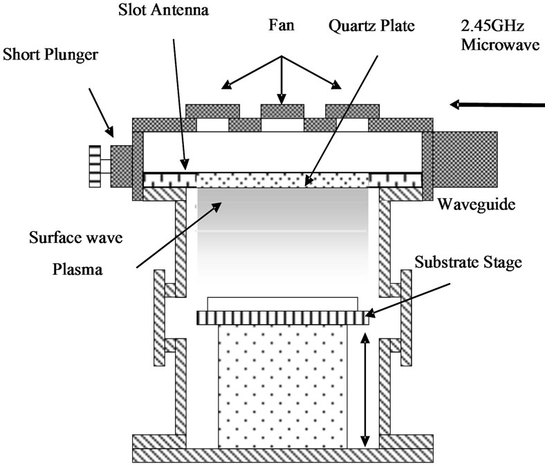
Figure 1. Schematic diagram of the MW SWP CVD system.
1011 cm−3 is formed in the vacuum chamber and broadened in the downstream region due to particles diffusion. Unlike other plasma sources the SWP is a promising plasma source for large-area thin film deposition and useful to avoid plasma induced damages of the substrates surfaces. Before deposition substrates were cleaned with acetone and methanol and only for Si substrates were etched with diluted hydrofluoric acid (HF:H2O) (1:10) in order to remove the native oxide layer from the surface, detail of this is described elsewhere [27]. For film deposition, acetylene (C2H2 = 50 sccm), Argon (Ar = 280 sccm) and trimethylboron (B(CH3)3 = 3 sccm) were used for source, carrier and dopant gas respectively. The MW power was set at 1300 W and a constant working pressure was maintained approximately at 60 Pa during deposition. The deposition chamber was evacuated to a base pressure approximately at 2 ´ 10−4 Pa using turbo pumps.
The deposited films were characterized by X-ray photoelectron spectroscopy (XPS), Hall Effect measurement, JASCO V-570 UV/VIS/NIR spectroscopy, Raman spectroscopy, Transmission Electron Microscopy (TEM) and JASCO SS-200 W solar simulator at room temperature (25˚C) in dark and under AM 1.5 simulated solar radiation.
3. Results and Discussion
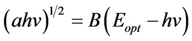
Chemical compositional analysis of the incorporated boron into the a-C (a-C:B) film was performed by XPS measurement (SSX-100) utilizing Al Kα (hν = 1486.6 eV) radiation. Figure 2 shows typical XPS spectrum of the a-C film. The XPS spectrum of the B doped film shows the presence of B, indicating the successful incorporation of B (0.35 at. %) in the film. In this work, we found high concentration of B into the film compared to that of our previous work [28] but we believed that the doping efficiency is to be low. The detail quantitative study about the chemical composition of B incorporated a-C film is underway. Furthermore, the result of Hall effects measurement has confirmed that the B is incorporated in the film; (the film is p-type semiconducting in nature). From the measurements of optical reflectance and transmittance, the optical band gap of the a-C thin film was determined by the Tauc relation [29],
where B is the density of the localization state constant and Eopt is the optical gap obtained from the extrapolation of the linear part of the curve at the absorption coefficient α = 0. The result showed that the optical band gap of the film is 1.2 eV. The absorption coefficient (α) (104 ~ 105 cm−1) of the film is calculated by the spectral reflectance and transmittance and films thickness data.
The structural morphology of the a-C film was characterized by transmission electron microscopy (TEM). Figure 3 shows the some graphene layers (17 - 18 layers) are grown inside the a-C film. In the inset of the fi-
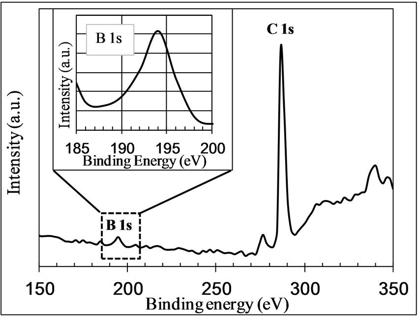
Figure 2. Core level X-ray photoelectron spectrum of carbon (C 1s) and boron (B 1s) for the a-C film. The inset shows the highly magnified boron peak.
Figure 3. TEM image of the film shows some graphene layers (17 - 18 layers) that are grown in the a-C film. In the inset, the intensity pattern of the graphene layers is presented.
gure, the intensity pattern of the graphene layers (an interplanar spacing is about 0.35 nm) is shown. It corresponds to the graphite spacing [30]. Raman spectrum shows a good agreement of graphene structure formation into the carbon film.
Raman spectroscopy is widely used for the analysis of carbon and carbon-related materials [31,32]. Raman scattering is used as a powerful technique to understand the microstructure changes of a-C films. Raman spectrum provided a wide range of structure and phase disorder information. The C-C bonding configurations are deduced from the Raman scattering spectrum analysis. The analysis of such spectrum is usually made by drawing an analogy with graphite [33]. Raman spectrum show a main peak centered at approximately 1580 cm−1 (known as G peak), which corresponds to the only Raman-active mode in mono-crystalline graphite (stretching vibration mode of the C=C double bond in the plane of hexagonal layers), while the low wave structure is related to the disorder-induced centered at approximately 1350 cm−1 (known as D peak), which appears in micro-crystalline or defective graphite.
Figure 4 shows Raman spectrum of a-C film, performed at room temperature. Major three peaks known as D, G and 2D peaks are clearly observed and centered at approximately 1351.4 cm−1, 1580.4 cm−1 and 2701.2 cm−1 respectively. It is reported that the D-peak represents disordered sp2-hybridized carbon with an amount of sp3-hybrodized carbon, while the G-peaks represents graphite-like sp2-hybridized carbon in the deposited film [34]. The presence of 2D peak shows a good agreement of graphene structure formation inside the a-C film.
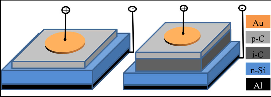
The purpose of this work is to deposit semiconducting a-C film applicable for photovoltaic solar cells. JASCO SS-200W solar simulator was used to measure photovoltaic characteristics of the a-C thin film based solar cells. Figure 5 shows a schematic diagram of two configurations, namely (a) p-C/n-Si and (b) p-C/i-C/n-Si (by inserting i-C layer (110 nm) between p-C and n-Si). The
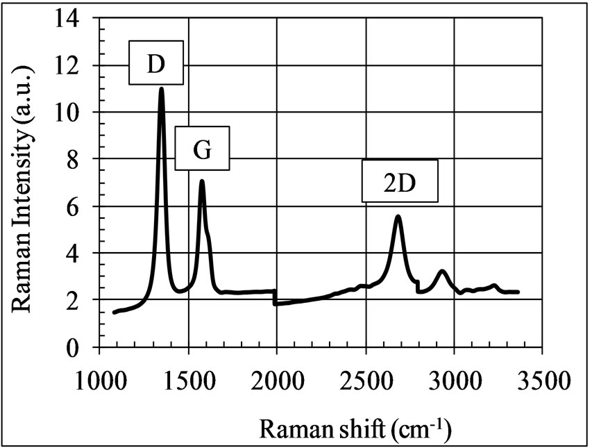
Figure 4. Raman spectrum of a-C film.
front and back contacts of the cells were made with semitransparent gold (Au) (~30 nm) and gold antimony (AuSb) (~100 nm) respectively.
Current-voltage (I-V) characteristics of the above configurations; (p-C/n-Si and p-C/i-C/n-Si) under dark and illumination are shown in Figure 6. Both configurations showed rectifying curve in dark [18,20] indicating the formation of a heterojunction solar cell between p-C film and n-type silicon. When illuminated by the light, the both configuration showed photovoltaic behavior; maximum open-circuit voltage (Voc), short circuit current density (Jsc), fill factor (FF) and conversion efficiency (η) are summarized in Table 1.
It is observed that the device (p-C/i-C/n-Si) inserted intrinsic carbon film (110 nm) between p-C and n-Si ex-
 (a) (b)
Figure 5. Schematic diagram of the p-C/n-Si (a) and p-C/iC/n-Si (b) heterojunction carbon based solar cells.
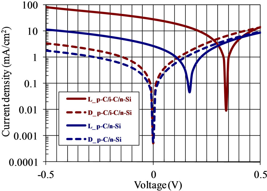
Figure 6. The Current-voltage characteristics of the p-C/nSi and p-C/i-C/n-Si heterojunction carbon based solar cells under dark and light illumination (AM 1.5, 100 mW/cm2).
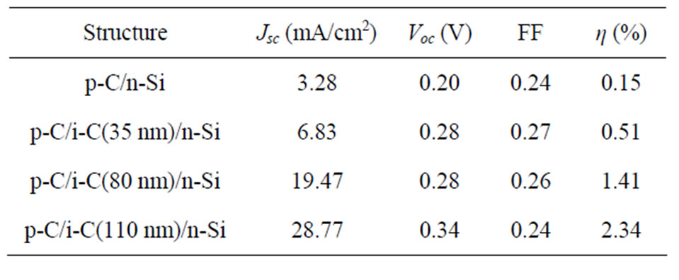
Table 1. Photovoltaic parameters of two heterojunction carbon solar cells of different configurations (p-C/n-Si and p-C/i-C/n-Si).
hibited significant enhancement of photovoltaic characteristics over the device (p-C/n-Si). In addition, we prepared three different devices (p-C/i-C/n-Si) with different intrinsic layer thickness (35 ~ 110 nm) for reference. The results (Table 1) show that the current density increased with increasing thickness of the intrinsic layer. This is attributed to increase photo absorption, better carrier separation and transport and reduce defect of interface region due to the intrinsic layer. The conversation efficiency of the solar cells is still low due to high defect density and recombination on the surface and inside the a-C. In addition, incident light energy loss occurred inside the electrode (light is absorbed by gold film) [35]. Thus, a large portion of the light generated electron-hole pairs will combine at the surface and inside the a-C films, and only a few of them can contribute to the energy conversion. The preliminary results show that the power conversation efficiencies of the solar cells are low. However, the results can be important references for further development of reasonably high efficiency a-C thin film based solar cells.
The quantum efficiency (QE) of the solar cells configurations; p-C/n-Si and p-C/i-C/n-Si are shown in Figure 7. Both configurations (p-C/n-Si and p-C/i-C/n-Si) have wide range of wavelength from 300 nm to almost 1000 nm. It is clear that the QE of configuration p-C/i-C/n-Si has improved significantly compared to that of p-C/n-Si configuration due to the absorption of intrinsic layer.
4. Conclusion
Carbon thin films deposited on Si and quartz substrate by microwave surface wave plasma CVD, using Acetylene, Argon and trimethyl boron as source, carrier and dopant gases. The structural and electrical properties of the films were investigated by the standard characterization techniques. Boron incorporation in the film has been conformed by XPS measurement. Structural properties of the
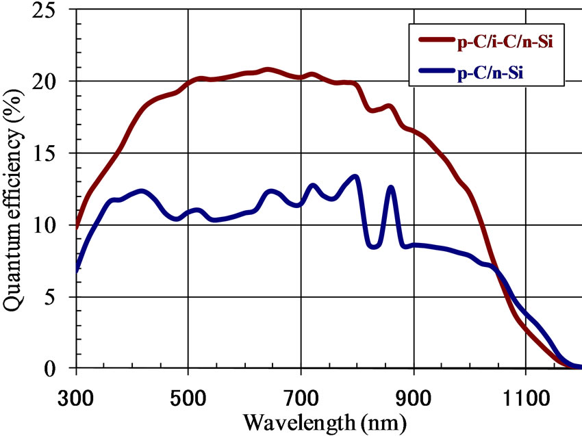
Figure 7. The spectral photoresponse characteristics of p-C/ n-Si and p-C/i-C/n-Si heterojunction carbon based solar cells.
films were characterized by TEM and Raman. We fabricated four types of photovoltaic solar cells of configuration p-C/n-Si and p-C/i-C/n-Si (i-C film thickness; 35, 85 and 110 nm) and characterized their photovoltaic properties. All the configurations displayed photovoltaic behavior under dark and light illumination. The device (p-C/iC/n-Si) inserted intrinsic carbon film between p-C and n-Si exhibited significant enhancement of the photovoltaic characteristics over the device without intrinsic layer (p-C/n-Si). In addition, the current density is increased with increasing intrinsic layer (i-C) thickness.
5. Acknowledgements
We thank Mr. Kawahara for helping us to measure TEM image of the carbon films.
REFERENCES
- M. Krishna, T. Soga, T. Jimbo and M. Umeno, “A Phosphorus Doped (n-Type) Carbon/Boron Doped (p-Type) Silicon Photovoltaic Solar Cell from a Natural Source,” Carbon, Vol. 37, No. 3, 1999, pp. 531-533. doi:10.1016/S0008-6223(99)00019-6
- M. Umeno and S. Adhikary, “Diamond-Like Carbon Thin Films by Microwave Surface-Wave Plasma CVD Aimed for the Application of Photovoltaic Solar Cells,” Diamond and Related Materials, Vol. 14, No. 11-12, 2005, pp. 1973-1979. doi:10.1016/j.diamond.2005.09.030
- M. Krishna, Y. Nukaya, T. Soga, T. Jimbo and M. Umeno, “Solar Cells Based on Carbon Thin Films,” Solar Energy Materials and Solar Cells, Vol. 65, No. 1-4, 2001, pp. 163-170. doi:10.1016/S0927-0248(00)00091-X
- X. Wang, H. R. Harris, K. Bouldin, H. Temkin, S. Gangopadhyay, M. D. Strathman and M. West, “Structural Properties of Fluorinated Amorphous Carbon Films,” Journal of Applied Physics, Vol. 87, No. 1, 2000, pp. 621-623. doi:10.1063/1.371910
- H. Kiyota, K. Okano, T. Iwasaki, H. Izumiya, Y. Akiba, T. Kurosu and M. Iida, “Fabrication of Metal-InsulatorSemiconductor Devices Using Polycrystalline Diamond Film,” Japanese Journal of Applied Physics, Vol. 30, No. 12A, 1991, pp. 2015-2017. doi:10.1143/JJAP.30.L2015
- J. W. Glesener, A. A. Morrish and K. A. Snail, “A ThinFilm Schottky Diode Fabricated from Flame-Grown Diamond,” Japanese Journal of Applied Physics, Vol. 70, No. 9, 1991, pp. 5144-5146. doi:10.1063/1.348992
- S. M. Mominuzzaman, K. M. Krishna, T. Soga, T. Jimbo and M. Umeno, “Raman Spectra of Ion Beam Sputtered Amorphous Carbon Thin Films Deposited from Camphoric Carbon,” Carbon, Vol. 38, No. 1, 2000, pp. 127-131. doi:10.1016/S0008-6223(99)00107-4
- T. Soga, T. Jimbo, K. M. Krishna and M. Umeno, “Amorphous Carbon Thin Films for Optoelectric Device Application,” International Journal of Modern Physics B, Vol. 14, No. 2-3, 2000, pp. 206-217. doi:10.1142/S0217979200000200
- H. G. Chun, J. H. Lee, Y. Z. You, Y. D. Ko, T. Y. Cho, K. V. Oskomov, N. S. Sochugov and A. N. Zakharov, “Pulsed Magnetron Sputtering Deposition of DLC Films. Part II: High-Voltage Bias-Assisted Deposition,” Journal of Korean Institute of Surface Engineering, Vol. 36, No. 2, 2003, pp. 148-154.
- D. T. Peeler and P. T. Murray, “Dynamics of Amorphous Carbon Film Growth by Pulsed Laser Deposition: Kinetic Energy of the Incident Particles,” Diamond and Related Materials, Vol. 3, No. 8, 1994, pp. 1124-1127. doi:10.1016/0925-9635(94)90105-8
- F. Y. Chuang, C. Y. Sun, T. T. Chen and I. N. Lin, “Local Electron Field Emission Characteristics of Pulsed Laser Deposited Diamond Like Carbon Films,” Applied Physics Letters, Vol. 69, No. 23, 1996, p. 3504. doi:10.1063/1.117226
- Rusli, G. A. J. Amaratunga and S. R. P. Silva, “Photoluminescence in Amorphous Carbon Thin Films and Its Relation to the Microscopic Properties,” Thin Solid Films, Vol. 270, No. 1-2, 1995, pp. 160-164. doi:10.1016/0040-6090(95)06911-9
- J. Robertson, “Deposition Mechanism of a-C and a-C:H,” Journal of Non-Crystalline Solids, Vol. 164-166, Pt. 2, 1993, pp. 1115-1118.
- M. Matsuoka and K. Ono, “Low-Energy Ion Extraction with Small Dispersion from an Electron Cyclotron Resonance Microwave Plasma Stream,” Applied Physics Letters, Vol. 50, No. 26, 1987, p. 1864. doi:10.1063/1.97719
- Y. Inoue, T. Komoguchi, H. Nakata and O. Takai, “Synthesis of Sn-doped a-C:H Films by RF Plasma-Enhanced Chemical Vapor Deposition and Their Characterization,” Thin Solid Films, Vol. 322, No. 1-2, 1998, pp. 41-45. doi:10.1016/S0040-6090(97)00937-1
- Y. Hayashi, G. Yu, M. M. Rahaman, K. M. krishna, T. Soga, T. Jimbo and M. Umeno, “Spectroscopic Properties of Nitrogen Doped Hydrogenated Amorphous Carbon Films Grown by Radio Frequency Plasma-Enhanced Chemical Vapor Deposition,” Journal of Applied Physics Vol. 89, No. 12, 2001, pp. 7924-7931. doi:10.1063/1.1371268
- K. M. Krishna, Y. Nukaya, T. Soga, T. Jimbo and M. Umeno, Technical Digest PVSEC-11, Hokkaido, 1999, p. 309.
- X. M. Tian, M. Rusop, Y. Hayashi, T. Soga, T. Jimbo and M. Umeno, “A Photovoltaic Cell from p-Type BoronDoped Amorphous Carbon Film,” Solar Energy Materials and Solar Cells, Vol. 77, No. 1, 2003, pp. 105-112. doi:10.1016/S0927-0248(02)00461-0
- M. Rusop, S. M. Mominuzzaman, T. Soga and T. Jimbo, “Photovoltaic Properties of n-C:P/p-Si Cells Deposited by XeCl Eximer Laser Using Graphite Target,” Solar Energy Materials and Solar Cells, Vol. 90, No. 18-19, 2006, pp. 3205-3213. doi:10.1016/j.solmat.2006.06.018
- X. M. Tian, T. Soga, T. Jimbo and M. Umeno, “The a-C:H/p-Si Solar Cell Deposited by Pulse Laser Deposition,” Journal of Non-Crystalline Solids, Vol. 336, No. 1, 2004, pp. 32-36. doi:10.1016/j.jnoncrysol.2003.12.045
- D. R. McKenzie, “Tetrahedral Bonding in Amorphous Carbon,” Reports on Progress in Physics, Vol. 59, 1996, p. 1611. doi:10.1088/0034-4885/59/12/002
- Z. Q. Ma and B. X. Liu, “Boron-Doped Diamond-Like Amorphous Carbon as Photovoltaic Films in Solar Cell,” Solar Energy Materials and Solar Cells, Vol. 69, No. 4, 2001, pp. 339-344. doi:10.1016/S0927-0248(00)00400-1
- V. S. Veerasamy, G. A. J. Amaratunga, C. A. Davis, A. E. Timbs, W. I. Milne and D. R. McKenzie, “n-Type Doping of Highly Tetrahedral Diamond-Like Amorphous Carbon,” Journal of Physics: Condensed Matter, Vol. 5, No. 13, 1993, pp. L169-L174. doi:10.1088/0953-8984/5/13/004
- K. Kadas, G. G. Ferenczy and S. Kugler, “Theory of Dopant Pairs in Four-Fold Coordinated Amorphous Semiconductors,” Journal of Non-Crystalline Solids, Vol. 227, Pt. 1, 1998, pp. 367-371. doi:10.1016/S0022-3093(98)00228-2
- M. T. Kuo, P. W. May, A. Gunn, M. N. R. Ashfold and R. K. Wild, “Studies of Phosphorus Doped Diamond-Like Carbon Films,” Diamond and Related Materials, Vol. 9, No. 3-6, 2000, pp. 1222-1227. doi:10.1016/S0925-9635(99)00305-2
- M. Nagatsu, T. Sano, N. Takada, N. Toyoda, M. Tanga and H. Sugai, “Characteristics of Hydrogenated Amorphous Carbon Films Deposited by Large-Area Microwave-Sustained Surface Wave Plasma,” Diamond and Related Materials, Vol. 11, No. 3-6, 2002, pp. 976-979. doi:10.1016/S0925-9635(01)00616-1
- S. Adhikari, S. Adhikary, A. M. M. Omer, M. Rusop, H. Uchida, T. Soga and M. Umeno, “Optical and Structural Properties of Amorphous Carbon Thin Films Deposited by Microwave Surface-Wave Plasma CVD,” Diamond and Related Materials, Vol. 15, No. 2-3, 2006, pp. 188-192. doi:10.1016/j.diamond.2005.08.069
- S. Adhikari, D. C. Ghimire, H. R. Aryal, S. Adhikary, H. Uchida and M. Umeno,” Boron-Doped Hydrogenated Amorphous Carbon Films Grown by Surface-Wave Mode Microwave Plasma Chemical Vapor Deposition,” Diamond and Related Materials, Vol. 15, No. 11-12, 2006, pp. 1909-1912. doi:10.1016/j.diamond.2006.07.022
- J. Tauc, “Amorphous and Liquid Semiconductors,” Plenum Press, London, New York, 1974, Chapter 4. doi:10.1007/978-1-4615-8705-7
- G. E. Bacon, “The Interlayer Spacing of Graphite,” Acta Crystallographica, Vol. 4, Pt. 6, 1951, pp. 558-562. doi:10.1107/S0365110X51001781
- D. S. Knight and W. B. White, “Characterization of Diamond Films by Raman Spectroscopy,” Journal of Materials Research, Vol. 4, No. 2, 1989, pp. 385-393. doi:10.1557/JMR.1989.0385
- S. R. P. Silva, J. Robertson, G. A. J. Amaratunga, B. Rafferty, L. M. Brown, J. Schwan, D. F. Franceschini and G. Mariotto, “Nitrogen Modification of Hydrogenated Amorphous Carbon Films,” Journal of Applied Physics, Vol. 81, No. 6, 1997, p. 2626. doi:10.1063/1.363927
- M. A. Tamor and W. C. Vassell, “Raman ‘Fingerprinting’ of Amorphous Carbon Films,” Journal of Applied Physics, Vol. 76, No. 6, 1994, p. 3823. doi:10.1063/1.357385
- R. O. Dillon, J. A. Woollam and V. Katkanant, “Use of Raman Scattering to Investigate Disorder and Crystallite Formation in As-Deposited and Annealed Carbon Films,” Physical Review B, Vol. 29, No. 6, 1984, pp. 3482-3489. doi:10.1103/PhysRevB.29.3482
- H. A. Yu, T. Kaneko, S. Yoshimura and Y. Suhng, “The Spectro-Photovoltaic Characteristics of a Carbonaceous Film/n-Type Silicon (C/n-Si) Photovoltaic Cell,” Applied Physics Letters, Vol. 69, No. 26, 1996, pp. 4078-4080. doi:10.1063/1.117824
NOTES
*Corresponding author.