Journal of Crystallization Process and Technology
Vol. 2 No. 4 (2012) , Article ID: 23435 , 4 pages DOI:10.4236/jcpt.2012.24020
Preparation and Performance Research of CuInSe2 Materials Applied in Solar Cell
![]()
1School of Information Science and Technology, Northwest University, Xi’an, China; 2School of Materials Science and Engineering, University of Science and Technology Beijing, Beijing, China; 3Department of Electrical and Computer Engineering, McGill University, Montreal, Canada.
Email: wangxuew@nwu.edu.cn
Received July 3rd, 2012; revised August 13th, 2012; accepted September 1st, 2012
Keywords: Solar Cell; CuInSe2; Resistivity; Ultraviolet-Visible Spectrum
ABSTRACT
At present, CuInSe2 (referred to as CIS) semiconductor has become one of the hot points in solar cell field at home and abroad for its excellent performances, such as direct bandgap, high light absorption coefficient, high photoelectric conversion efficiency and long-term stability. In this paper, the CIS bulk materials are prepared by the horizontal Bridgman method with double-heat sources, the crystal structure, microstructure morphology and composition of the samples are analyzed in X-ray diffraction instrument (XRD) and scanning electronic microscope (SEM) with Energy Dispersive X-ray Spectrum (EDX), and surface electrical state and electrical properties of the samples are characterized in X-ray photoelectron spectroscopy (XPS) and four point resistivity test system. The results show that the CIS crystal was grown, and that the conductive performance of the samples is good which display the characteristics of p-type semiconductor. Furthermore, a thin film CIS sample was obtained by argon ion-beam scanning bombardment, and it has high solar energy absorptivity and the bandgap of 0.99 eV analyzed in Ultraviolet-visible Spectrum that is suitable for solar cell.
1. Introduction
The solar energy has become the focus of new energy and renewable energy development because of its cleanness and security features. At present, photovoltaic power generation materials applied in solar cells include the following: simple substance materials such as silicon, polysilicon, amorphous silicon, and compounds such as GaAs, CdS, CuInSe2 and so on [1,2]. However, the corresponding photovoltaic products have various problems such as cost, pollution, mass production, efficiency etc when used for solar energy conversion devices. For example, Ga, As and Cd elements are toxic and very expensive. In addition, some organic materials [3,4] are low-cost, flexible, easy to be machined as solar cell, but the lifetime of organic cells is very short. The CIS is a direct bandgap semiconductor with chalcopyrite structure at room temperature, and has high absorption rate of sunlight and collection of minority carriers, and then the CIS thin film has strong anti-radiation capacity, low cost, good thermal stability [5], so that it is regarded as the one of the most promising solar cell materials [6]. Although the preparation techniques of CIS thin film have many, including the vacuum evaporation method, the molecular beam epitaxy, the magnetron sputtering method, the spray pyrolysis method, the screen printing method, the electrodeposition method and so on, the speed of the methods is slow and the cost is very high [7-9]. Therefore, CIS materials used for high efficient solar cell are prepared with batch-growth and low-cost horizontal Bridgman method in this paper, and their microstructure and optoelectronic properties are analyzed [10] in order to provide actual and significant data for the preparation of the solar cells with high efficiency and low cost.
2. Experiments
By using a horizontal Bridgman method with two temperature zones (referred to 2T-HB), the mixture of Cu and In powder at the standard stoichiometric ratio of 12 g and Se powder of 1.5 g are tiled on both ends of the high and low temperature zones of the quartz tube respectively, and the quartz tube is welded hermetically when evacuated to 5 × 10⁻⁴ Pa. The high temperature zone is heated to about 1370 K (1050˚C) to melt the mixture, and the low-temperature region is heated to a temperature corresponding with the desired resultant pressure of 67 Pa - 1.013 × 10⁵ Pa. After it is kept for 12 hours, the quartz tube is dragged horizontally to the low temperature zone in the speed of 5 mm/h. Thus, the samples are obtained after cooled to room temperature, and the resultant pressures growing Sample 1 and Sample 2 are 260 Pa and 280 Pa separately [11].
3. Characterizations and Analysis
3.1. Phase Analysis
The XRD pattern of Sample 1 is shown in Figure 1, there are three phases in Sample 1, which are CuSe, CuSe2O5 and CIS crystals respectively, and the unmarked peaks in the pattern belong to the peaks of Se crystal that account for superfluous Se is diffused into sample1. And there are two phases in XRD pattern of Sample 2 (shown in Figure 2), which are CuSe2 and CIS crystals respectively.
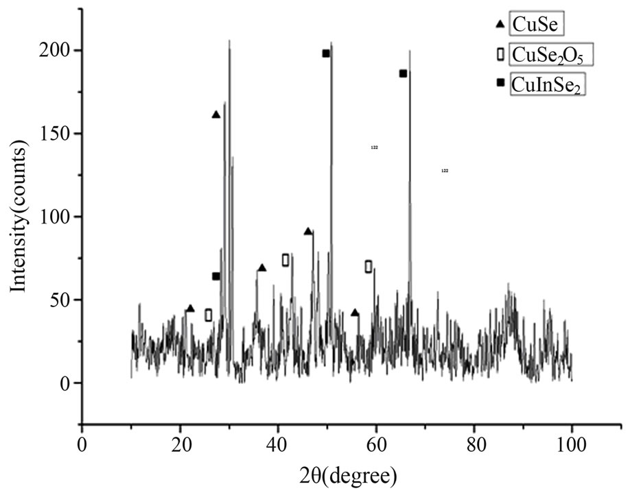
Figure 1. XRD pattern of Sample 1.
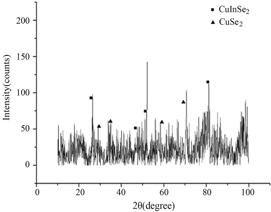
Figure 2 XRD patterns of Sample 2.
3.2. Surface Morphology and Elemental Distribution Analysis
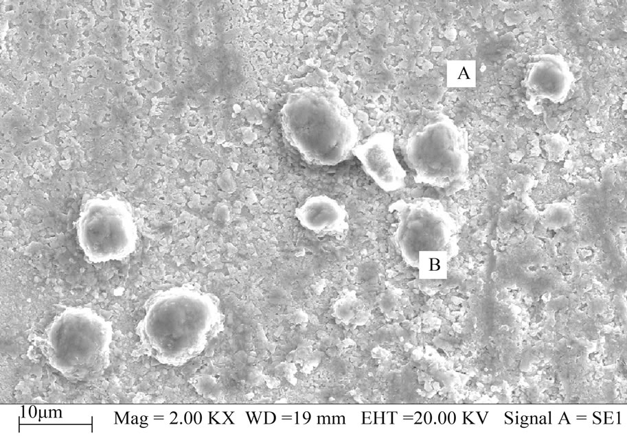
3.2.1. The SEM Characterization of Sample 1
Figure 3 is the SEM micrographs of Sample 1 in LEO- 1450-SEM. In Figure 3(a), some spherical objects marked as B are distributed in uniform and close substrate region marked as A, and the diameter of the Bs ranges from 5 μm to 10 μm. In Figure 3(b), the grains of region A are well-proportioned and neat-ranged, and region A has darker smoothing matrix phase marked as C and lighter color round particles marked D, and then the Bs are gathered and stacked by some large grains than C.
From the EDX spectrum of the B in Sample 1, the analysis results show that the components of the B only contain Cu and Se, no In, and the atomic ratio of Cu and Se is about 1:1. Combined with the above XRD results, the B can be determined as CuSe phase. Similarly, that grain C contains Cu, In, Se elements can be found at an atomic ratio of about 1:1:2, and the matrix phase C is the atomic ratio of 2.14:4.28:1, and D is the mixture of CuSe2O5 with CIS phase.
 (a)
(a)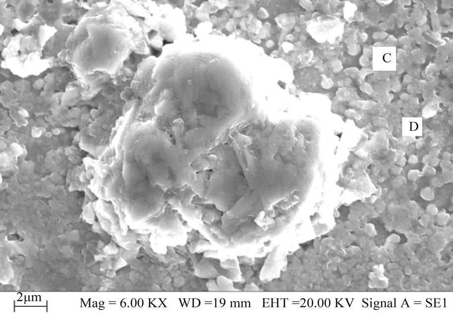 (b)
(b)
Figure 3. The SEM micrographs of Sample 1 (a) Overall micrograph at 2000 times; (b) Magnification micrograph of B at 6000 times.
3.2.2. The SEM Characterization of Sample 2
Figure 4 is the SEM micrographs of Sample 2. The uniform matrix is labeled as E, in which some triangle grains (labeled as F) of 3 μm - 10 μm are irregularly distributed. By analyzing EDX, the matrix E contains Cu, In, Se elements at the atomic ratio of 1.13:1:3.69, and is known as selenium-rich CIS phase, and then the triangular particle F has two elements Cu and Se at the atomic ratio of about 1:2 which is CuSe2 phase.
Comparing the results of the two Samples, it turns out that the morphology uniformity of Sample 2 is better than that of Sample 1, and both the spherical objects CuSe phase in Sample 1 and the triangular particles CuSe2 in Sample 2 make the surface uneven, and then CuSe2O5 phase in Sample1 shows that Sample 1 is weakly oxidized.
3.3. XPS Analysis of the Samples
By using an AXIS-165-type XPS of Japan, overall XPS spectra of Sample 1 in 0 eV - 1000 eV is gotten in Figure 5. In which, the characteristic peaks of Cu element can be seen in 920 eV - 960 eV, In element in 440 eV - 456 eV, and Se element in 44 eV - 60 eV and O element
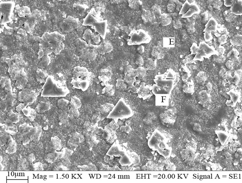
Figure 4. SEM photograph of the Sample 2.
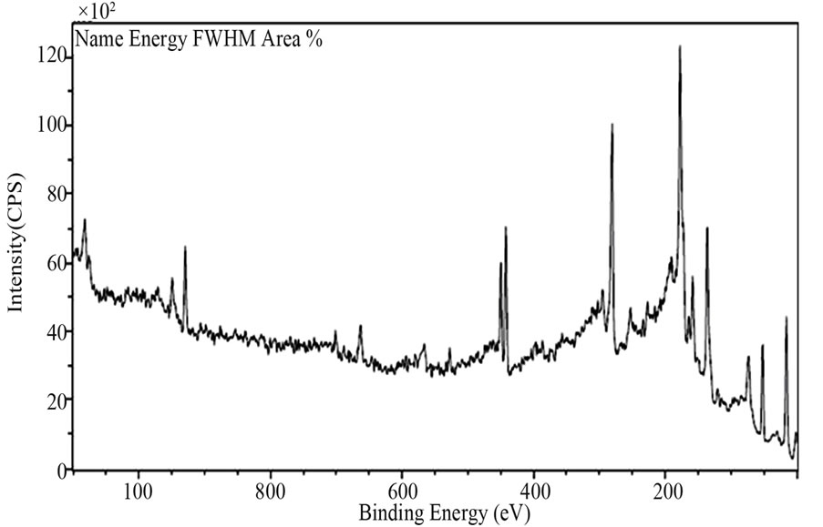
Figure 5. The XPS spectrum of sample1 in binding energy range of 0 - 1000 eV.
in 520 eV - 536 eV, and then C element is in 272 eV - 292 eV which may be the reasons of carbon pollution in the process and the surface pollution exposed to the air. Furthermore, the percentages of the elements contained in the test point can be got as Cu2p 0.98%, In3d 2.09%, Se3d 10.40%, O1s 2.23% and C1s 84.30%.
Similarly the percentage of the elements in Sample 2 can be obtained as Cu2p 6.8%, In3d 11.31%, Se3d 11.77%, O1s 22.95% and C1s 47.17%. By comparison, Sample 1 has a deeper selenation level, which is probably because the CuSe phase in Sample 1 has a more loose structure than CuSe2 phase in Sample 2 so that it can promote the diffusion of Se in the selenizing process.
3.4. The Electrical Properties of CIS
The resistivity of the block of Sample 1 cut into a thickness d of 1.16 mm is measured by four-probe method. On the reverse side of the sample, let the straight line connected by the four-point probes be parallel to the boundary of Sample 1 with a distance L of 1.48 mm, and the correction coefficient from the experiment manual is looked up, and then the relation of current and voltage is measured so as to calculate the resistivity. The average resistivity ρ of the different points of Sample 1 is 55.72 Ω∙mm. Similarly, Sample 2 is sliced into a bulk, and the average resistivity of the points is 11.58 Ω∙mm.
It turns out that the resistivity of Sample 2 is much smaller than that of sample1. Combined with the previous results, the semiconductor Se, CuSe and CuSe2O5 [12], and metal CuSe2 [13] is just right the reason that the resistivity of Sample 2 is smaller.
3.5 The Optical Performance of CIS
Owing to influence of Se [12] and C on optical performance, the thin film of Sample 2 with a thickness of 1.5 μm is formed by being scanningly bombarded with Ar ion beams, and the absorptivity of the thin film in wavelength range of 200 nm - 2500 nm is measured with Cary 5000 Ultraviolet and Visible Spectroscopy (UV-Vis), and CIS films in the visible band (390 nm - 770 nm) show extremely good absorption, and the absorptivity at 339 nm reaches 0.93, and then the relation curve between the absorption coefficient α and the photon energy hγ of the CIS film is calculated.
By using the direct bandgap transition equation that CIS film satisfied, which is the relationship between absorption coefficient and the photon energy 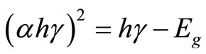 , the relation curve
 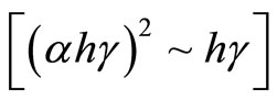 can be drawn in Figure 6. In theory, there should be a straight line, which intercept on the
  horizontal ordinate is the optical bandgap of the film and is about 0.99 eV, and matches the optical bandgap that is about 0.89 eV to 1.02 eV with the sunlight reported in the literature.
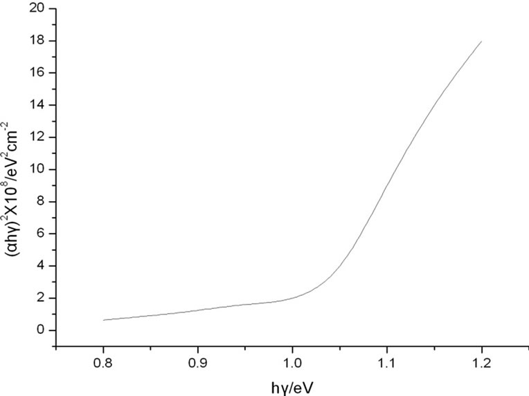
Figure 6. The relation curve  of CIS thin films.
4. Conclusions
After characterizing and analyzing performance of two samples, the conclusions are reached as follows.
1) There are three phases in Sample 1 which are CuSe, CuSe2O5, and CIS, and there are two phases in Sample 2 which are CuSe2 and CIS. The CuSe and CuSe2O5 of Sample 1 are formed due to low pressure, and the CuSe2 of Sample 2 is brought out by the high pressure, so the pressure to prepare CIS should be in the middle.
2) The average resistivity of Sample 2 measured by the four-probe method is smaller, which is led to by CuSe2.
3) The as-prepared CIS thin film has a high light absorptivity in the visible band, and has relatively approximate bandgap to the optimum value of the photovoltaic conversion. Therefore CIS is very suitable for a high efficient solar cell.
5. Acknowledgements
One of us (all authors) thanks the support of the National Science Foundation (61076002) and Shaanxi Education Commission (2010 JK848).
REFERENCES
- M. A. Green, K. Emery, Y. Hishikawa and W. Warta, “Solar Cell Efficiency Tables (Version 37),” Progress in Photovoltaics: Research and Applications, Vol. 19, No. 1, 2011, pp. 84-92. doi:10.1002/pip.1088
- N. B. Chaure, J. Young and A. P. Samantilleke, “Electrodeposition of p-i-n Type CuInSe2 Multilayers for Photovoltaic Applications,” Solar Energy Materials & Solar Cells, Vol. 81, No. 1, 2004, pp. 125-133. doi:10.1016/j.solmat.2003.10.001
- J. M. Sun, Y. X. Zhu, X. F. Xu, L. F. Lan, L. J. Zhang, P. Cai, J. W. Chen, J. B. Peng and Y. Cao, “High Efficiency and High Voc Inverted Polymer Solar Cells Based on a Low-Lying HOMO Polycarbazole Donor and a Hydrophilic Polycarbazole Interlayer on ITO Cathode,” The Journal of Physical Chemistry C, Vol. 116, No. 27, 2012, pp. 14188-14198. doi:10.1021/jp3009546
- G. Adolf and H. Christopher, “Photovoltaic Materials, Past, Present, Future,” Solar Energy Materials and Solar Cells, Vol. 62, No. 1, 2000, pp. 1-19. doi:10.1016/S0927-0248(99)00131-2
- G. P. Vassilev, P. Docheva and N. Nancheva, “Technology and Properties of Magnetron Sputtered CuInSe2 Layers,” Materials Chemistry and Physics, Vol. 82, No. 3, 2003, pp. 905-910. doi:10.1016/j.matchemphys.2003.08.005
- G. F. Zheng and H. X. Yang, “A Novel Semiconductor CIGS Photovoltaic Material and Thin Film ED Technology,” Chinese Semiconductors, Vol. 22, No. 11, 2001, pp. 1357-1363.
- R. Caballero and C. Guillen, “CuInSe2 Formation by Selenization of Sequentially Evaporated Metallic Layers,” Solar Energy Materials & Solar Cells, Vol. 86, No. 1, 2005, pp. 1-10. doi:10.1016/j.solmat.2004.05.019
- A. Ashour, A. A. S. Akla and A. A. Ramadan, “Study of Polycrystalline CuInSe2 Thin Film Formation,” Thin Solid Films, Vol. 467, No. 1, 2004, pp. 300-307. doi:10.1016/j.tsf.2004.04.046
- K. Subbaramaiah, “Structural and Optical Properties of Spray Deposited CIS Thin Films,” Solar Energy Materials and Solar Cells, Vol. 32, No. 1, 1994, pp. 1-6. doi:10.1016/0927-0248(94)90250-X
- A. H. Moharram, M. M. Hafiz and A. Salem, “Electrical Properties and Structural Changes of Thermally Co-Evaporated CuInSe2 Films,” Applied Surface Science, Vol. 172, 2001, pp. 61-67. doi:10.1016/S0169-4332(00)00836-9
- M. V. Yakushev, A. V. Mudryi and V. F. Gremenok, “Influence of Growth Conditions on the Structural Quality of Cu(In-Ga)Se2 and CuInSe2 Thin Films,” Thin Solid Films, Vol. 452, 2004, p. 133. doi:10.1016/j.tsf.2003.11.003
- A. Zegadi, M. V. Yakushev and E. Ahmed, “Effect of Se Content on Defect Levels in CuInSe2 Single Crystals Detected by Photoacoustic Spectrometry,” IEEE Photovoltaic Specialists Conference, Waikoloa, 5-9 December 1994.
- Z. F. Hou, A. Y. Li, Z. Z. Zhu and M. C. Huang, “Ab initio Calculation of the Electronic Structures of Copper Pyrites CuS2, CuSe2 and CuTe2,” Journal of Materials Science & Technology, Vol. 29, No. 4, 2004, pp. 429-431.