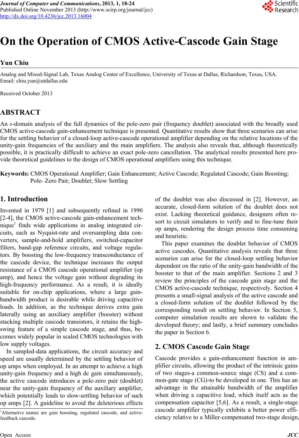
 Journal of Computer and Communications, 2013, 1, 18-24 Published Online November 2013 (http://www.scirp.org/journal/jcc) http://dx.doi.org/10.4236/jcc.2013.16004 Open Access JCC On the Operation of CMOS Active-Cascode Gain Stage Yun Chiu Analog and Mixed-Signal Lab, Texas Analog Center of Excellence, University of Texas at Dallas, Richardson, Texas, USA. Email: chiu.yun@utdallas.edu Received October 2013 ABSTRACT An s-domain analysis of the full dynamics of the pole-zero pair (frequency doublet) associated with the broadly used CMOS active-cascode gain-enhancement technique is presented. Quantitative results show that three scenarios can arise for the settling behavior of a closed-loop active-cascode operational amplifier depending on the relative locations of the unity-gain frequencies of the auxiliary and the main amplifiers. The analysis also reveals that, although theoretically possible, it is practically difficult to achieve an exact pole-zero cancellation. The analytical results presented here pro- vide theoretical guidelines to the design of CMOS operational amplifiers using this technique. Keywords: CMOS Operational Amplifier; Gain Enhancement; Active Cascode; Regulated Cascode; Gain Boosting; Pole- Zero Pair; Doublet; Slow Settling 1. Introduction Invented in 1979 [1] and subsequently refined in 1990 [2-4], the CMOS active-cascode gain-enhancement tech- nique1 finds wide applications in analog integrated cir- cuits, such as Nyquist-rate and oversampling data con- verters, sample-and-hold amplifiers, switched-capacitor filters, band-gap reference circuits, and voltage regula- tors. By boosting the low-frequency transconductance of the cascode device, the technique increases the output resistance of a CMOS cascode operational amplifier (op amp), and hence the voltage gain without degrading its high-frequency performance. As a result, it is ideally suitable for on-chip applications, where a large gain- bandwidth product is desirable while driving capacitive loads. In addition, as the technique derives extra gain laterally using an auxiliary amplifier (booster) without stacking multiple cascode transistors, it retains the high- swing feature of a simple cascode stage, and thus, be- comes widely popular in scaled CMOS technologies with low supply v oltages. In sampled-data applications, the circuit accuracy and speed are usually determined by the settling behavior of op amps when employed. In an attempt to achieve a high unity-gain frequency and a high dc gain simultaneously, the active cascode introduces a pole-zero pair (doublet) near the unity-gain frequency of the auxiliary amplifier, which potentially leads to slow-settling behavior of such op amps [2]. A guideline to avoid the deleterious effects of the doublet was also discussed in [2]. However, an accurate, closed-form solution of the doublet does not exist. Lacking theoretical guidance, designers often re- sort to circuit simulators to verify and to fine-tune their op amps, rendering the design process time consuming and heuristic. This paper examines the doublet behavior of CMOS active cascodes. Quantitative analysis reveals that three scenarios can arise for the clos ed-loop settling behavior dependent on the ratio of the unity-gain bandwidth of the booster to that of the main amplifier. Sections 2 and 3 review the principles of the cascode gain stage and the CMOS active-cascode technique, respectively. Section 4 presents a small-signal analysis of the active cascode and a closed-form solution of the doublet followed by the corresponding result on settling behavior. In Section 5, computer simulation results are shown to validate the developed theory; and lastly, a brief summary concludes the paper in Section 6. 2. CMOS Cascode Gain Stage Cascode provides a gain-enhancement function in am- plifier circuits, allowing the product of the intrinsic gains of two stages-a common-source stage (CS) and a com- mon-gate stag e (CG)-to be developed in one. This has an advantage in the attainable bandwidth of the amplifier when driving a capacitive load, which itself acts as the compensation capacitor [5,6]. As a result, a single-stage cascode amplifier typically exhibits a better power effi- ciency relative to a Miller-compensated two-stage design, 1Alternative names are gain boosting, regulated cascode, and active- 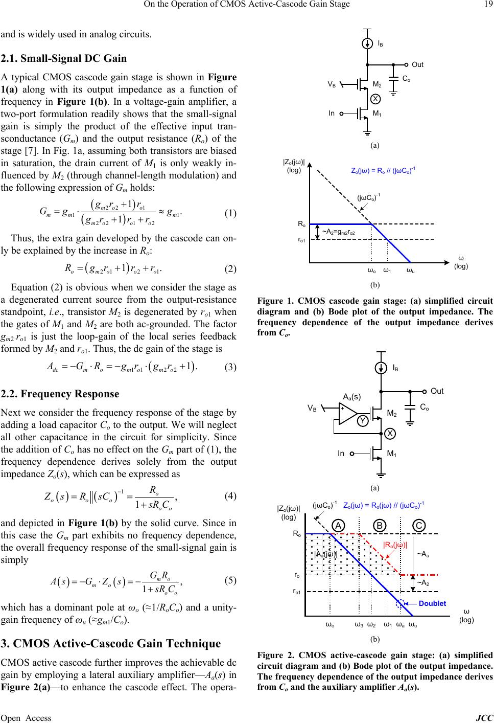 On the Operation of CMOS Active-Cascode Gain Stage Open Access JCC and is widely used in analog circuits. 2.1. Small-Signal DC Gain A typical CMOS cascode gain stage is shown in Figure 1(a) along with its output impedance as a function of frequency in Figure 1(b). In a voltage-gain amplifier, a two-port formulation readily shows that the small-signal gain is simply the product of the effective input tran- sconductance (Gm) and the output resistance (Ro) of the stage [7]. In Fig. 1a, assuming both transistors are biased in saturation, the drain current of M1 is only weakly in- fluenced by M2 (through channel-length modulation) and the following ex pression of Gm holds: ( ) ( ) 22 1 11 221 2 1. 1 mo o mm m moo o gr r Gg g grr r + =⋅≈ ++ (1 ) Thus, the extra gain developed by the cascode can on- ly be explained by the increase in Ro: ( ) 212 1 1. omooo Rgrr r= ++ (2) Equation (2) is obv ious when w e consider th e stage as a degenerated current source from the output-resistance standpoint, i.e., transistor M2 is degenerated by ro1 when the gates of M1 and M2 are both ac-grounded. The factor gm2·ro1 is just the loop-gain of the local series feedback formed by M2 and ro1. Thus, the dc gain of the stage is ( ) 1122 1. dcmom omo AG Rgrgr=−⋅=− ⋅+ (3) 2.2. Frequency Response Next we consider the frequency response of the stage by adding a load capacitor Co to the output. We will neglect all other capacitance in the circuit for simplicity. Since the addition of Co has no effect on the Gm part of (1), the frequency dependence derives solely from the output impedance Zo(s), which can be expressed as ( )() 1, 1o o oo oo R Z sRsCsR C − == + (4) and depicted in Figure 1(b) by the solid curve. Since in this case the Gm part exhibits no frequency dependence, the overall frequency response of the small-signal gain is si mp ly ( )( ) , 1 mo mo oo GR AsGZ ssR C =−⋅ =− + (5 ) which has a dominant pole at ωo (≈1/RoCo) and a unity- gain frequency of ωu (≈gm1/Co). 3. CMOS Active-Cascode Gain Technique CMOS active cascode further improves the achievable dc gain by employing a lateral auxiliary amplifier—Aa(s) in Figure 2(a)—to enhance the cascode effect. The opera- (a) (b) Figure 1. CMOS cascode gain stage: (a) simplified circuit diagram and (b) Bode plot of the output impedance. The frequency dependence of the output impedance derives from Co. (a) (b) Figure 2. CMOS active-cascode gain stage: (a) simplified circuit diagram and (b) Bode plot of the output impedance. The freque ncy dependence of t he output impedanc e derives from Co and the auxiliary amplifier Aa(s). ω (log) |Z o (jω)| (log) r o1 R o ω 1 ω o ω u Z o (jω) = R o // (jωC o ) -1 (jωC o ) -1 ~A 2 =g m2 r o2 |A a (jω)| ω (log) ~A a r o1 r o R o ω o ω a ω 3 ω 1 ω 2 ω u Z o (jω) = R o (jω) // (jωC o ) -1 |R o (jω)| (jωC o ) -1 AB C |Z o (jω)| (log) ~A 2 Doublet  On the Operation of CMOS Active-Cascode Gain Stage Open Access JCC tion principles of the technique can be explained as fol- lows. 3.1. Output Resistance and Gain At this point, we understand that the extra voltage gain of the normal cascode stage in Figure 1(a) derives from the improved output resistance due to the local series feed- back formed by M2 and ro1. Therefore, additional gain can be potentially obtained by further increasing either gm2 or ro1. The active-cascode technique exploits the gm2 option as shown in Figure 2(a). Let’s consider the effec- tive transconductance of M2 due to the presence of the auxiliary amplifier. The gate-source voltage of M2 is 0 − vx = −vx and vy − vx = −( Aa + 1)vx before and after the booster insertion, respectively. Therefore, the net effect of the booster is essentially to make the effective tran- sconductance of M2 (Aa + 1) times larger, with every- thing else being equal between Figures 1(a) and 2(a). Thus, the dc solution to the active-cascode amplifier of Figure 2(a) can be readily obtained by substituting (Aa+1)gm2 for gm2 in (1)-(3): ( ) ( ) 22 1 11 221 2 11 , 11 a moo mm m amooo A grr Gg g Agrr r ++ =⋅≈ + ++ (6) ( ) 2121 1 1, oamoo o RAgrr r=+++ (7) ( ) 112 2 1 1. dcm oamo Agr Agr=− ⋅++ 2 (8) We see that the key function of the booster is to en- hance gm2, hence to further increase the output resistance (and gain) of the amplifier.3 This is done by introducing a push-pull operation between the source and gate voltages of M2, i.e., between nodes X and Y, through the insertion of a booster amplifier. This inevitably introduces another negative feedback loop that is local to the cascode M2. As the bandwidth of the booster amplifier is finite, the fre- quency response of the active cascode exhibits an inter- esting artifact—a pole-zero pair or frequency doublet, which wi l l be explained next. 3.2. Frequency Doublet For simplicity, we will assume a single-pole roll-off for the auxiliary amplifier: (9) Therefore, the frequency dependence of the gain stage can be readily obtained by replacing Aa with Aa(s) in (6)-(8). The effect of Aa(s) on the output resistance was quali- tatively analyzed in [2], which is sketched in Figure 2(b). Let’s examine Ro first. The roll-off of Aa(s) at high fre- quency introduces frequency dependence of Ro as illu- strated by the dash-dotted curve in Figure 2(b), mathe- matically, ( )( ) 212 12 1. oam oooo RsA sgrrrr= +++ (10 ) In Figure 2(b), ro = gm2ro1ro2 + ro1 + ro2, which can al- so be obtai ne d from (10) by set ting Aa(s) to 0. Thus, Ro(s) exhibits a pole at ω3 and a zero at ωa in Figure 2(b). Th e overall output impedance of the stage Zo(s) is then the parallel combination of Ro(s) and (sCo)−1, (11) which is represented by the solid curve in Figure 2(b). An equivalent RC model of Zo(s) wa s proposed i n [8], which is sketched in Figure 3. If we divide the frequency axis into three bands by ω3 and ωa in Figure 2(b), the left resistor Aaro in Figure 3 captures the low-frequency output resistance in region A (ω ≤ ω3), the middle series RC network captures the roll-off part of Ro(s) in region B (ω3 ≤ ω ≤ ωa) and the flat part in region C (ω ≥ ωa), and lastly the right Co represents the shunt load capacitor. In regions A and B, an approximate expression of the out- put impe dance is (12) where, x = ω3/ωo = ωa/ω2. Obviously, this only results in one pole at ωo. In regions B and C, an approximate ex- pression of the out put i mpedanc e is given by ( ) 1 1. 1 1 oo oo oo ooo rC s xx Zs rrC sC sCsC s xx + ≈+ = ++ (13) Apparently, this results in two poles and on e zero, with a pole at and a zero at —both are very close to the unity-gain frequency of the booster ωa when x>>1 ho lds. This is the pole-zero pair or doublet. Figure 3. Model of the output impedance of the active cas- code in Figure 2. 2The body effect of M2 can be readily inclu ded in (6)- the dc gain is ( ) { } 11222 11 dcm oammbo AgrAg g r=−⋅ +++ effect. 3 A similar argument also suggests that the technique works only for MOSFET, not BJT amplifiers, in that the base resistance o ultimately limit the achievable amplifier output resistance to approx- imately β0ro, where β0 is the small-signal current gain of the BJT, re- gardless of the value of Aa.  On the Operation of CMOS Active-Cascode Gain Stage Open Access JCC 3.3. Slow Settling In [9-11], a closed-loop amplifier containing a closely spaced pole-zero pair in its frequency response was ex- amined. It was found th at, although the doublet effect on the open-loop Bode plot is often negligible, its delete- rious impact on the time-domain settling behavior may be significant. Specifically, it introduces a so-called slow- settling component to the step response of the am- plifier. The magnitude of the slow component is propor- tional to the doublet spacing and the time constant cor- responds to the double t frequency. The same line of development will be followed here to establish a framework for the next two sections. Let the open-loop transfer function have a closely spaced pole- zero pair at (ωz, ωp). The dominant pole and unity-gain frequencies, ωo and ωu, respectively, are given for the open-loop response. When the loop is closed, the feed- back will reduce the pole-zero spacing by an amount equal to the loop-gain at the doublet frequency; and the closed-loop pole frequency will move to ωp' [10,11]. With the assumption ωo << (ωz, ωp) << βωu, the step response of the closed-loop amplifier is given as ( ) () ' 12 1, p u t t o V tVkeke ω βω − − ≈− + (14 ) where, β is the feedback factor, and '2 1 ,. zp zp pz z uz u k ωω ωω ωω ω βω ωβω −− ≈+≈ ≈ − (15) The k2 term in (14) is the slow-settling component when ωp' < βωu holds. 4. Solving Doublet For the CMOS active cascode, although the approximate equivalent circuit model of Zo(s) in Section 3.2 reveals the existence of a pole-zero pair near the unity-gain fre- quency of the auxiliary amplifier ω a, the results are only qualitative as the frequency dependence of Gm(s) is not considered in the model. In this section, we will attempt to obtain an exact small-signal solution for the doublet. In the treatment, the frequency dependence of the circuit is assumed to derive from the load capacitor Co and the booster Aa(s); and all other capacitances will be neglected first to keep the math tractable. After the first -order pole- zero behavior is derived, the effects of other capacitances in the circuit will be examined in Section 5 using com- puter simulation. 4.1. Open-Loop Transfer Function To solve for the open-loop transfer function, we first obtain the expressions for Gm(s) and Zo(s): ( )( ) ( ) ( ) ( ) 22 1 1 221 2 11 , 11 amo o mm amoo o As grr Gs gAsgrr r ++ =⋅ + ++ (16) ( )( )( ) ( ) 1. 1 o oo o oo Rs Zs RssCsC Rs == + (17) The product of (16) and (17) gives the small-signal voltage gain in (18) (see below), where A1 = gm1·ro1, A2 = gm2·ro2, and the expression of Aa(s) in (9) is assume d. 4.2. Frequency Doublet The numerator of (18) readily solves to one LHP zero: 2 2 1. 1 z aa a A sAA ωω =− +≈− + (19) To solve for the poles, we define γ = ro2/ro1, ωu = gm1/Co, and ro1 = A1/Coωu; the denominator of (18) reduc- es to the following: ( ) ( )( ) ( ) 2 2 2 12 12 11 11 0. 1 au a a ua a AA ss AA AA AA A γω ω γγ ωω γ + ++ ++ ++ ++ += ++ (20) Due to the presence of the doublet, we may assume that one pole is at sp1 = −αωa with α ≈ 1; and (20) can be factorized into ( )( ) 12 0. 1 u a a ss AAA ω αω αγ + ⋅+= ++ (21) Compare (21 ) with (20), we o bt a i n ( ) 2 2 12 1 1, 11 au aa a A A AAAA A ω αγ γω − ≈ ++ ++ ++ (22) where, is assumed since x >> 1. At this point, we arrive at the solution for the two LHP poles of the open -loop transfer function: ( )( ) 1 12 , 11 1 u po u aa a sAA AA ωω ω γω −≈ ≈ +++ +− (23) ( ) 2 2 2 12 1 1, 11 a pa ua aa A A sAAAA A ω ωω γγ − −≈+ +≈ ++ ++ (24) ( )( )( )( ) ( ) ( ) ( )( ) ( ) ( ) ( ) 12 21 21 2 2 122 12 1 11 11 . 11 111 a a aa mo oo aa aoo ooo o aa AA A AAA s As A A AsGs ZssC RsAA AAr rCsArrCs ω ωω + + ++ ++ = ⋅== + ++++++ ++ (18)  On the Operation of CMOS Active-Cascode Gain Stage Open Access JCC where, the fact x = ω3/ωo>>1 is again assumed. 4.3. Closed-Loop Settling Behavior We recognize that sp1 of (23) is the dominant pole of the open-loop amplifier and (sz, sp2) of (19) and (24) form a doublet. Substituting (19) and (24) in (15) results in an expression for the slow-settling component: (25) ()( )( ) 2 2 2 212 1 1. 11 1 aa ua A A kAAAA A ω γ βγω γ − ≈− + ++++ (26) Equation (26) reveals that three scenarios can arise for the closed-loop settling behavior dependent on ωa/ωu, the ratio of the unity-gain bandwidth of the auxiliary am- plifier to that of the open-loop main amplifier: 1) k2 = 0, critically damped, when ωu/ωa ≈ γA1 = gm1·ro2. The pole cancels the zero exactly and the slow-settling term vanishes; 2) k2 > 0, overshoot, when ωu/ωa < gm1·ro2. This results in a falling doublet; 3) k2 < 0, slow settling, when ωu/ωa > gm1·ro2. This re- sults in a rising doublet, the one often cited in the litera- ture [2]. In addition, as ωu = gm1/Co, the criterion ωu/ωa = gm1·ro2 leads to ωa = 1/ro2Co. In other words, even when a con- stant Co is assumed, the significant dependence of ro2 on the amplifier output voltage makes it practically difficult to achieve an exact pole-zero cancellation. There are two strategies to avoid the deleterious effect of the doublet. One suggests to make ωa > βωu to avoid slow settling [2]. The other suggests to make k2 small enough, i.e., to have a “slow-but-accurate” doublet. Let’s examine the feasibility of the latter. Assuming a very slow doublet, i.e., ωa << βωu holds, then following (26), (27) This implies that k2 cannot be made arbitrarily s mall— the smallest value of k2 is inversely proportional to the loop-gain of the main amplifier without gain enhance- ment. A “slow-but-accurate” doublet does not exist. 5. Computer Simulation Computer simulations have been performed to validate the analysis developed in Section 4. For easy access to and programmability of all device parameters, i.e., gm, ro, etc., a small-signal linear model of the active cascode shown in Figure 4 was used instead of a real transistor circuit. An ideal VCVS models the auxiliary amplifier with a transfer function Aa(s). In Figure 5, the external feedback is assumed ideal with a feedback factor β = 1/2 (i.e., the closed-loop gain is 2); and a 1-V step is applied at the input. A capacitor Cm on node X (resulting in the Figure 4. Small-signal model of the CMOS active cascode. A capacitor Cm on node X and the Cgs’ and Cgd’s of M1 and M2 are also included for second-order effects. (a) (b) Figure 5. (a) Closed-loop amplifier model and (b) the input voltage step used in simulation. second pole) and the Cgs’ an d Cgd’ s of M1 and M2 are also included for completeness. All device parameters used in the simulation are listed in Table 1. 5.1. Intrinsic Doublet Behavior To evaluate the intrinsic behavior of the doublet, all ca- pacitors are removed except Co in Figure 4; the uni- ty-gain frequency of Aa(s) is swept to observe the settling behavior of the closed-loop amplifier. Figures 6(a) and (b) show the output voltage and the normalized settling error of the circuit, respectively. The settling error is de- fined as ( )( )( ) ( ) , i o i Vt Vt tVt β δ β − = (28) It is apparent that indeed three scenarios for the set- tling behavior exist as predicted in Section 4.3. Specifi- cally, a critically damped output transient was observed confirming the possibility of an exact pole-zero cancella- tion. In the example used here, (26) predicts that k2 = 0 when fa = (2πro2Co)−1 ≈ 10 MHz; while computer simula- V o V 2 V 1 X Y r o2 C gs2 r o1 g m2 V 2 g m1 V 1 C o C gd2 C gd1 C m -A a (s) C gs1  On the Operation of CMOS Active-Cascode Gain Stage Open Access JCC Table 1. Small-signal parameters used in simulation. β 0.5 ro2 10 kΩ fu 200 MHz Cm Co/3 Aa 40 dB Cgs1 Co/6 gm1 2 mA/V Cgs2 Co/6 gm2 1 mA/V Cgd1 Co/12 ro1 10 kΩ Cgd2 Co/12 (a) (b) Figure 6. Closed-loop settling behavior for fa = 10 kHz, 100 kHz, 1 MHz, 5 MHz, 9 MHz, 10.95 MHz, 20 MHz, and 30 MHz: (a) the amplifier output voltage (increasing in fa from bottom up), and (b) the normalized settling error (increas- ing in fa from top down). Open-loop parameters: fa = 10 kHz, β fu = 100 MHz, and β Adc = 80 dB. The dashed curves (fa = 10.95 MHz) correspond to the case of k2 = 0, i.e., exact pole-zero cancellation. tion reveals that this actually occurs for fa ≈ 10.95 MHz. In addition, Figure 6(b) further indicates that, when the slow-settling component is really “slow” (ωa << βωu), the knee accuracy where the slow term starts to dominate is always nearly −40 dB, corresponding to k2 = 1/βAo = −0.01 as predicte d by (27). 5.2. Effect of the Second Pole A capacitor Cm at node X in Figure 4 is added to intro- duce a non-dominant pole with a frequency three times larger than βωu, the close-loop bandwidth (i.e., the phase margin of the loop-gain is around 71˚). The simulation results are shown in Figures 7 (a) and (b). The basic set- tling behavior is unaltered with the inclusion of the second pole; and the slow tails after the initial ov ershoots die out closely resemble those of the case with Cm = 0, especially when ωa << βωu holds. 5.3. Effect of Other Parasitics The Cgs’ and Cgd’s of the transistors M1 and M2 are fur- ther included to make the small-signal model complete. Reasonably large values for these capacitors are assumed (Table 1), and the simulation results are shown in Fig- ures 8(a) and (b). Again, the behavior of the slow-set- tling component is seemingly independent of the various second-order effects introduced by the parasitics. An exact pole-zero cancellation always o ccurs for fa ≈ 10.95 MHz. In [2], the criterion βωu < ωa < ωp2 was proposed to ensure proper operation of the active cascodes. This is verified in simulation by keeping Cm constant while stepping ωa up to and beyond ωp2. Figure 9 illustrates (a) (b) Figure 7. The same results as those of Figure 6 with the inclusion of Cm. The phase margin of the loop-gain is 71˚. The dashed curves are for Cm = 0. The basic settling beha- vior remains the same in the presence of a second pole.  On the Operation of CMOS Active-Cascode Gain Stage Open Access JCC (a) (b) Figure 8. The same results as those of Figure 6 with the inclusion of Cm and the Cgs’ and Cgd’s of M1 and M2. The slow tails of the transients closely resemble those of the original case (the dashed curves) in spite of the initial sig- nificant overshoots. Figure 9. The normalized settling error for fa = 10.95 MHz (dashed curve), 100 MHz, and 1 GHz with fp2 ≈ 300 MHz. that sluggish settling o ccurs when ωa is in the vicinity of ωp2, where the local feedback loop formed by the booster and the cascode becomes marginally stable. The instabil- ity is lifted when ωa is further pushed out (not shown in the figure). 6. Summary An accurate, closed-form s-domain analysis and comput- er simulation results of the pole-zero pair (doublet) asso- ciated with the widely used CMOS active-cascode gain stage are presented. The conventional picture of “slow settling” is clarified and augmented with a set of equa- tions that completely describe the doublet dynamics. These results provide easy-to-follow guidelines to the design of such amplifiers in practice. 7. Acknowledgements This work was inspired by a conversation took place between the author and Klaas Bult at UCLA in 1996. The sma ll -signal solution of the doublet was developed in 1997. REFERENCES [1] B. J. Hosticka, “Improvement of the Gain of MOS Am- plifiers,” IEEE Journal of Solid-State Circuits, Vol. 14, No. 6, 1979, pp. 1111-1114. http://dx.doi.org/10.1109/JSSC.1979.1051324 [2] K. Bult and G. J. G. M. Geelen, “A Fast-Settling CMOS Op Amp for SC Circuits with 90-dB DC Gain,” IEEE Journal of Solid-State Circuits, Vol. 25, No. 6, 1990, pp. 1379-1384. http://dx.doi.org/10.1109/4.62165 [3] E. Sackinger and W. Guggenbuhl, “A High-Swing, High-Impedance MOS Ca sc ode Circui t,” IEEE Journal of Solid-State Circuits, Vol. 25, No. 1, 1990, pp. 289-298. http://dx.doi.org/10.1109/4.50316 [4] H. C. Yang and D. J. Allstot, “An Active-Feedback Cas- code Current Source,” IEEE Transactions on Circuits and Systems, Vol. 37, No. 5, 1990, pp. 644-646. http://dx.doi.org/10.1109/31.55008 [5] P. R. Gray and R. G. Meyer, “MOS Operational Amplifi- er design—A Tutorial Overview,” IEEE Journal of Sol- id-State Circuits, Vol. 17, No. 6, 1982, pp. 969-982. http://dx.doi.org/10.1109/JSSC.1982.1051851 [6] A. A. Abidi, “On the Operation of Cascode Gain Stages,” IEEE Journal of Solid-State Circuits, Vol. 23, No. 6, 1988, pp. 1434-1437. http://dx.doi.org/10.1109/4.90043 [7] P. R. Gray, P. J. Hurst, S. H. Lewis and R. G. Meyer, “Analysis and Design of Analog Integrated Circuits,” 4th Edition, Wiley, New York, 2001. [8] K. Bult, “EE215A Course Notes,” UCLA, 1996. [9] F. D. Waldhauer, “Analog Integrated Circuits of Large Bandwidth,” IEEE International Convention Record, Vol. 11, Part 2, 1963, pp. 200-207. [10] P. R. Gray and R. G. Meyer, “Recent Advances in Mono- lithic Operational Amplifier Design,” IEEE Transactions on Circuits and Systems, Vol. 21, No. 3, 1974, pp. 317-327. http://dx.doi.org/10.1109/TCS.1974.1083851 [11] B. Y. T. Kamath, R. G. Meyer and P. R. Gray, “Rela- tionship between Frequency Response and Settling Time of Operational Amplifiers,” IEEE Journal of Solid-State Circuits, Vol. 9, No. 6, 1974, pp. 347-352. http://dx.doi.org/10.1109/JSSC.1974.1050527
|