Open Journal of Applied Biosensor, 2013, 2, 104-111
Published Online November 2013 (http://www.scirp.org/journal/ojab)
http://dx.doi.org/10.4236/ojab.2013.24014
Open Access OJAB
A Low-Power CMOS Analog Front-End IC with
Adjustable On-Chip Filters for Biosensors
Donald Y. C. Lie1,2, Vighnesh Das1, Weibo Hu1, Yenting Liu1, Tam Nguyen1,2
1Department of Electrical and Computer Engineering, Texas Tech University, Lubbock, USA
2Department of Surgery, Texas Tech University Health Sciences Center, Texas Tech University, Lubbock, USA
Email: donald.Lie@ttu.edu
Received August 26, 2013; revised October 16, 2013; accepted October 24, 2013
Copyright © 2013 Donald Y. C. Lie et al. This is an open access article distributed under the Creative Commons Attribution License,
which permits unrestricted use, distribution, and reproduction in any medium, provided the original work is properly cited.
ABSTRACT
This paper presents a low-power CMOS analog front-end (AFE) IC designed with a selectable on-chip dual AC/DC-
coupled paths for bio-sensor applications. The DC-coupled path can be selected to sense a biosignal with useful DC
information, and the AC-coupled path can be selected for sensing the AC content of the biosignal by attenuating the
unwanted DC component. The AFE IC includes a DC-coupled instrumentation amplifier (INA), two variable-gain
1st-order low pass filters (LPF) with tunable cut-off frequencies, a fixed gain 2nd-order Sallen-Key high-pass filter (HPF)
with tunable cut-off frequencies, a buffer and an 8-bit differential successive approximation register (SAR) ADC. The
entire AFE channel is designed and fabricated in a proprietary 0.35-µm CMOS technology. Excluding an external
buffer needed to properly drive the ADC, the measured AFE IC consumes only 2.37 µA/channel with an input referred
noise of ~40 µVrms in [1 Hz, 1 kHz], and successfully displays proper ECG (electrocardiogram) and electrogram (EGM)
waveforms for QRS peaks detection. We expect that the low-power dual-path design of this AFE IC can enable it to
periodically record both the AC and the DC signals for proper sensing and calibration for various bio-sensing applica-
tions.
Keywords: Low-Power CMOS; Bio-Sensor Applications; DC-Coupled
1. Introduction
Wearable sensors are widely used to monitor patients’
medical/health conditions, and can provide quantitative
data for clinical use. Some applications only need the AC
information of the recorded bio-signals, such as the QRS
peak detection in the ECG signal for heart-rate monitor-
ing, but other applications such as temperature or pres-
sure sensing may require the DC information of the
bio-signals. As shown in Figure 1, a typical analog front-
end (AFE) circuit for a bio-sensor can have an instru-
mentation amplifier (INA), a filter, a variable gain am-
plifier (VGA) and an analog-to-digital converter (ADC)
[1-5]. Different applications may require the AFE cir-
cuits to implement the filters and the VGAs differently.
For example, in [1,2], independent blocks are used to
implement filters while in [3] the filter is implemented
inside an INA with balanced tunable large pseudo-re-
sistors to form a tunable bandwidth front-end amplifier
(TB-FEA). An important feature in recently reported
AFE circuits for biomedical applications is that a high-
Figure 1. A typical and simplified system block diagram of
the AFE (Analog Front-End) circuits for a generic bio-sen-
sors.
pass filter (HPF) is usually placed before an INA to re-
move the DC voltages, especially due to the concerns of
large DC offsets across differential electrodes that can be
caused by the electrochemical effects at the electrode-
tissue interface that can saturate the subsequent AFE
circuitry [2-5]. The HPF can be made on-chip or off-chip.
An external low-frequency HPF would use large discrete
off-chip capacitor(s) which are nuisances for implantable
bio-sensors as they prevent: 1) device size miniaturiza-
tion; 2) high reliability & manufacturability; 3) cost re-
duction; and 4) minimize noise coupling (external spuri-
ous noise pickup). The on-chip HPF can be made of
D. Y. C. LIE ET AL. 105
MOS pseudo resistors and capacitors [6]. However, to
the authors knowledge, most of the implantable medical
devices products today such as the pacemakers or im-
plantable cardioverter defibrillators (ICDs) still use these
large off-chip capacitors, partly due to the long approval
processes the regulatory agencies (e.g., the FDA) require
the medical devices manufacturers to go through with
prolonged clinical trials and testing.
In the applications where the DC voltages can contain
useful information, such as for continuous ECG/EEG
monitoring, good contact resistance on each electrode is
needed at all time, and therefore periodic checking and
calibration of the contact resistance and DC offset volt-
ages on each sensor node are needed to ensure monitor-
ing quality and to reduce the common-mode noise level.
Therefore, in order to effectively digitize both the sig-
nal’s DC and AC components for applications such as
continuous ECG/EEG monitoring and/or with additional
temperature sensing, we introduce in Figure 2 a design
option for the AFE circuits with dual AC-coupled and
DC-coupled paths. The AFE IC can be switched periodi-
cally to check the contact resistance and the DC offset
voltages of each electrode or between any pairs of elec-
trodes. Having the selectable band-pass filter entirely in-
tegrated on-chip ensures the output will mainly include
the signal we intend to pick up. For example, when we
are monitoring an ECG waveform, the readout does not
show the results of the muscular movement involved in
respiration. We believe our low-power dual-path AFE IC
can therefore be used in practical bio-sensors with a very
Figure 2. The proposed system block diagram of our dual-
path AFE integrated circuit (IC). The DC-coupled path:
INA + 1st LPF + BUFFER + ADC, and the AC-coupled path:
INA + 1st LPF + HPF + 2nd LPF + BUFFER + ADC. The
DC-coupled path and the AC-coupled path share the INA +
1st LPF. The AC-coupled path is selected here in this figure.
Each LPF can provide additional voltage gain with variabi-
lity. To simplify the system block diagram, a on-chip HPF
of a sub-Hz cut-off frequency that can filter out the poten-
tially large DC offsets is not put in the front of the proposed
AFE IC here.
small and competitive form factor. Simulation and meas-
urement results will be presented in this paper to show
the effectiveness of this proposed design method. Section
2 in this paper discusses the system-level analysis for the
proposed AFE IC. Section 3 explains the design of each
block, including the INA design, the low-pass filter (LPF)
design with variable gains and tunable cut-off frequen-
cies, the high-pass filter (HPF) design with tunable cut-
off frequencies, the buffer design and the 8-bit differen-
tial successive approximation register (SAR) analog-to-
digital converters (ADC) design. Section 4 shows the
measurement results of each circuit block and the entire
AFE IC for both the AC and DC paths. We will conclude
in Section 5.
2. AFE IC System Analysis
Figure 1 shows a generic AFE IC architecture for a bio-
sensor AFE circuit. It does not have a high pass filter in
the front, and therefore it digitizes both the DC and AC
components of the bio-signal. Because both DC and AC
components are digitized and the DC component can be
much larger than AC component, in order to maintain the
enough resolution for the small AC component, the
ADC’s least-significant-bit (LSB) must be rather small.
In order to accurately sense the DC component, the INA
must have the small offset voltage in order to have high
sensitivity. Moreover, a large offset voltage in a high-
gain INA could saturate the INA and also the ADC [7].
The advantage of this AFE architecture in Figure 1 is
that it is generic such that it does not remove any infor-
mation in input signals. However, the shortcomings are
that a high-resolution ADC is needed (say 16 - 20 bits),
and that a low-offset INA is also needed, which means
the power consumption required for this AFE IC design
would be rather high (say over 500 μW/channel). An
external anti-aliasing filter is also often needed to pro-
vide good signal conditioning.
As shown in Figure 2, the proposed AFE IC system
diagram includes a DC-coupled INA, two 1st-order LPFs,
a 2nd-order HPF, a buffer, and an ADC. The prototype
INA has two gain options, 20 dB and 40 dB. Each vari-
able-gain LPF has tunable cut-off frequencies, where
three control signals are used to select ten options of
cut-off frequencies within the range of (38, 200) Hz in
the measurement, and another three control signals to
choose ten options of gain settings in the range of (0, 27)
dB. The HPF is a Sallen-Key filter with tunable cut-off
frequencies of 5 Hz and 11 Hz as indicated from the
measurement. The buffer converts a single-ended signal
to a differential signal to drive a differential 8-bit SAR
ADC.
Please note that even though a HPF of a sub-Hz cut-
off frequency that can filter out the potentially large DC
offsets due to electrode-tissue interface is not put in the
Open Access OJAB
D. Y. C. LIE ET AL.
106
front of the proposed AFE circuits shown in Figure 2, it
can still be added in front of the AFE IC using the
pseudo-resistors on-chip when the AC-only signals are
needed. We choose not to show that complication in Fig-
ure 2 just for simplicity. The INA used here is a resistor-
feedback DC-coupled amplifier. In this way, the INA
will amplify the bio-signal’s both DC and AC compo-
nents. After the INA, a variable-gain LPF is used to fur-
ther amplify the signal if needed. There are two paths
after the 1st LPF: one directly goes to the ADC; the other
goes to the HPF and the 2nd variable-gain LPF and then
to the ADC. The first path is the DC-coupled path while
the second one is the AC-coupled path. The advantage of
the proposed AFE architecture is that it can process both
types of bio-signals (note as mentioned above an addi-
tional HPF with sub-Hz cut-off frequency may need to be
switched in if the DC offset is too large, but no additional
circuit blocks are needed). The DC-coupled INA enables
the sensing of both the DC and AC components. The
variable-gain INA can prevent the INA from getting
saturated when DC component is large. The intermediate
HPF can remove the unwanted DC component, and al-
lows the following stages to only process the AC signal.
3. Circuit Designs
The proposed AFE IC has a DC-coupled INA, two
1st-order low-pass filters, a 2nd-order high-pass filter, a
buffer and a differential SAR ADC.
3.1. Instrumentation Amplifier Design
A differential difference amplifier (DDA) with a resistor
feedback network is used to implement the DC-coupled
INA [8]. To balance the trade-off between low noise vs.
low power consumption for the resistor values in the re-
sistor feedback network, the total resistance is selected as
10 M to achieve an input referred noise of 0.12 µV/
sqrt (Hz) in the worst case (when R1 is ~1 M), where
the current consumption in the resistor feedback network
is less than 0.1 µA. As shown in the Figure 3, the volt-
age across the resistor feedback network is:
1 2outinRR DC
VVVA
V (1)
where A is the INA gain. Equation (1) indicates that the
current consumption in the resistor-feedback network is
linearly proportional to input signals.
Figure 4 shows a three-stage DDA. The 1st and 2nd
stages provide the high gains required, and the 3rd stage
is a source follower to drive the resistor-feedback net-
work. The 1st and 2nd stages have two low-frequency
poles at their output nodes, respectively, and the 3rd
stage’s output node is a high-frequency pole. In order to
get a large phase margin, a Miller compensation capaci-
tor of about 2 pF is put between the 1st stage’s output
V1p
V1n
Vin
VDC
V2p
V2n
Vout
R1=1 or
0.1 Mohm
R2=10 Mohm
Figure 3. The proposed INA with the resistor feedback
network. “ VDC ” is the DC operating point.
C
C
Figure 4. The schematic of the proposed differential differ-
ence amplifier (miller cap Cc shown and highlighted here).
node and the 2nd stage’s output node. Therefore, the pole
at the 1st stage’s output node is pushed to be less than 1
Hz and becomes a dominant pole. The phase margin in
the SPICE simulation is about 57 degree at the close-loop
gain of 20 dB.
The INA gain is programmable to help prevent the
channel from being saturated when the offset voltage is
large. If the channel is not saturated, the influence from
the offset voltage on the AC path is very small; this is
expected because the following high pass filters will re-
move the amplified DC offset voltage. As for the DC
path, the DC offset voltage in the previous stages would
influence the accuracy of the measurement results. In
order to minimize the offset voltage in the INA, the sizes
of the input devices are designed to be large, equal to 32
m/4 m, and also the common centroid scheme is used
in the INA layout to reduce the process-induced offsets.
3.2. Filters Design
As shown in Figure 5, the LPF consists of an op-amp
and large value passive components. The large value re-
sistors and capacitors are provided by the proprietary
Open Access OJAB
D. Y. C. LIE ET AL. 107
0.35-µm CMOS technology. The gain of the LPF is:
112233
Gain Lf
4
L
LLLLLL
R
SRSRSRR
  (2)
The cut-off frequency of the LPF is:

3
112233
1
2π
dB
f
Lf L f LL
fSCSC SCR
 f
(3)
where SLX and SfX are the control signals.
As shown in the Figure 6, the Sallen-Key topology is
used to implement the 2nd-order Butterworth filter. The
high thermal noise of the large value resistor in the HPF
is attenuated by the high gain in the previous stages, and
thus has a very small contribution to the channel’s input
referred noise.
3.3. Buffer Design
In our current prototype version of the proposed AFE IC,
the on-chip buffer circuit does not work well for some
reasons, and therefore an external buffer is used instead
to perform the overall AFE IC channel measurements.
Figure 5. The proposed LPF with tunable gains and tunable
frequencies.
Figure 6. The proposed HPF with tunable cut-off frequen-
cies.
Note the issue of lack of drivability for the on-chip buffer
has been fixed as validated from separate measurement
data from subsequent tapeouts. The external buffer is
made of a unit-gain amplifier and a single-ended-to-di-
fferential converter to properly drive the differential
ADC. In this particular channel design, the output driv-
ing ability of the on-chip filter is small and therefore not
able to drive a resistive load of the external single-
ended-to-differential converter. Therefore, the filter is
connected to an external single-ended unit-gain amplifier
first and then the amplifier’s output signal is converted to
a differential signal by the external single-ended-to-dif-
ferential converter to drive a differential SAR ADC,
which design is to be discussed next.
3.4. SAR ADC Design
Considering the stringent requirement of the low power
consumption, a SAR ADC is selected here, rather than a
Sigma-Delta ADC which can perform better noise-sha-
ping [9]. As shown in Figure 7, a differential 8-bit SAR
ADC is designed. The DAC in the differential ADC uses
the monotonic switching method, because the capacitor
arrays with this switching method only use half capacitor
size and consume about 19% power during digitizing vs.
those with the traditional switching method [10].
4. Measurement Results
The entire AFE IC is designed and fabricated in a Texas
Instruments (TI) proprietary 0.35 µm Bipolar-CMOS-
DMOS process, while only the standard 0.35-µm 3 V
CMOS devices and the on-chip passive components were
used for this design. The die size is 3300 1300 µm2.
The micro-photograph of the die is shown in Figure 8.
Compared with the size of die, if we had chosen the AFE
IC architecture shown in Figure 1, the size of the AFF
IC with external resistors and capacitors would have
been much larger.
4.1. The INA Measurement Results
The prototype INA provides two gain options: 20 dB and
40 dB. The INA transfer function with the gain equal to
Figure 7. The block diagram of our proposed 8-bit differen-
tial SAR ADC.
Open Access OJAB
D. Y. C. LIE ET AL.
108
40 dB is shown in Figure 9. The INA output noise with
the gain of 40 dB is shown in Figure 10. The measured
noise is consistent with the simulated noise. As expected,
1/f noise dominates the output noise. Compared with the
noise of a normal op-amp, the DDA has two differential
input pairs, which would lead to relatively large input-
referred noise (IRN). To improve its noise performance,
a chopper-based INA with an order of magnitude IRN
reduction in simulation was designed and the results will
be reported in later publications.
4.2. Filter Measurement Results
The whole filter chain has two 1st-order LPFs and one
2nd-order HPF. The cut-off frequencies of LPFs and the
Figure 8. The micro-photograph of the whole AFE IC with-
out external buffers.
Figure 9. Measured transfer function of the INA.
Figure 10. The output noise of INA with the gain equal to 40
dB.
HPF are all tunable. The low pass RC filters also provide
variable gains. The filters’ tunable frequency ranges are
shown in the summary Table 1, and implemented using
capacitor banks controlled by external signals. As seen in
Figure 11, the cut-off frequencies of the entire filter
chain in the AC-coupled path are 5 Hz and 38 Hz, re-
spectively, and the attenuation slope is 40 dB/Dec.
4.3. ADC Measurement Results
Figure 12 shows the measured differential nonlinearity
Figure 11. The measured transfer function of the entire
filter chain in the AC-coupled path.
Table 1. Measured results summary of the proposed AFE
IC.
Power supply 2 V
INA current consumption 1.1 µA
INA input referred noise
22 µV @ 1 Hz
2 µV @ 100 Hz
350 nV @ 1 kHz
INA CMRR* 74 dB
INA gain 20 dB or 40 dB
INA DR 45 dB
INA bandwidth [DC, 878 Hz]
Filter current consumption 0.62 µA
Filter low cut-off frequency DC, 5.2, 11 Hz
Filter high cut-off frequency 38 - 200 Hz
Filter DR 51 dB
ADC current consumption 0.65 µA @ 2 kS/s
DNL/INL (0.62, 0.47)/(0.61, 0.47) LSB
ADC ENOB 7.4 bits
Total gain in DC-coupled path 20 - 66 dB
Total gain in AC-coupled path 20 - 92 dB
Die size 3300 1300 µm2
AFE IC current consumption** 2.37 µA/channel
*Common-mode rejection ratio; **Exclude the power consumption of the
external buffer.
Open Access OJAB
D. Y. C. LIE ET AL. 109
(DNL) and integral nonlinearity (INL) of the SAR ADC.
The DNL is measured in the range of 0.62/0.47 LSB
while the INL is within 0.61/0.47 LSB. Figure 13
shows the FFT with the input frequency of 0.2 kHz at 2
kS/s. The spurious free dynamic range (SFDR) is 58 dB,
and the single-to-noise-and-distortion-ratio (SNDR) is
46.2 dB, equivalent to an effective number of bits
(ENOB) of 7.4 bits.
4.4. Overall Measurement/Simulation Results
bio The signal from an interactive ECG simulator by Sym
Corporation is used to test the entire AFE circuits.
Among the different kinds of ECG signals, “NSR” signal
(normal sinus rhythm), which is the normal heart rate of
72 bpm, is fed into the AFE IC channel. The 3-lead ECG
measurement technique is used for the measurement.
“RL” (right leg) signal is connected to the AFE ground
as a reference voltage, and the “RA” (right arm) and
“LA” (left arm) signals are connected to the AFE’s INA
inputs. Both DC and AC information are tested to verify
the functionalities of the dual DC/AC-coupled paths (in
this case, ECG’s DC info is not useful). The AFE IC ex-
hibits a total gain in the DC-coupled path of 46 dB, with
20 dB in the INA and 26 dB in the first 1st-order LPF.
The AFE IC has a total gain of 66 dB in the AC-coupled
path when selected, with 40 dB in the INA and 26 dB in
the second 1st-order LPF. The AFE IC’s passband in the
AC-coupled path is set as [5,38] Hz. Figure 14 shows
the ECG measurement results. It can be seen that the
QRS complexes are very clear, which suggests the AFE
IC should be accurate enough for peak detection in pace-
makers and ICD applications as well as the intra-cardic
electrograms (EGMs) usually have higher magnitudes
than the surface ECG signals. Similar to the system si-
050100 150 200 250
-1
0
1
DNL (LSB)
050100 150 200 250
-1
0
1
Outpu t cod e
INL (LSB)
Figure 12. Measured DNL and INL of the ADC.
0100 200 300 400 500 600 700 800 9001000
-100
-80
-60
-40
-20
0
Frequency (Hz)
Amplitude (dB)
3rd harmoni cs
mulation performed in [2], the AFE IC without ADC is
simulated with patients’ EGM data (“iaf1_tva_CS90”)
[11]. As shown in Figure 15, our AFE IC design effec-
tively suppresses signals outside the band of [20, 105] Hz,
especially the T-wave occupying the frequency band
lower than 10 Hz to avoid mis-classifying the T-wave as
the QRS complex for proper pacermaker/ICD sensing of
the heartbeats. Note the unit for both Figures 14 and 15
is in Volt (V). The amplitudes in those figures can be
shown with negative values because these are the differ-
ential AC signals.
The detail measurement results of each block and the
AFE IC channel are shown in Table 1, which is consis-
tent of our design specification from SPICE simulations.
The measurement result of the DC path of the proposed
AFE IC with the input from the simulator is 0.44 V with
the total gain equal to 46 dB. The graphic presentation of
the measurement results of the DC path looks like a flat
line, and is therefore not shown here. In the DC-coupled
path for our proposed AFE IC, both AC and DC infor-
mation can go through AFE. For the DC path only 1st-
order LPF filter is used. In the AC-coupled path, ideally
only the AC information will go through, and the DC
information will be completely blocked by the high pass
filter. The high-pass filter is a 2nd order Sallen-Key filter
in the proposed AFE IC. Any leakage current through the
high-pass filter’s input capacitor would be converted by
the resistor in the feedback network and show up in the
filter’s output, which may be the main concern for the
DC signal leakage in the low-frequency high-pass filter.
The capacitor used in the proposed AFE is the poly ca-
pacitor, and the leakage current through the poly capaci-
tors is very small. Therefore, the DC energy leakage of
the capacitor/resistor is not significant in terms of signal
acquisition. The loss in the filter is mainly from intrinsic
012345678910
-0.1
0
0.1
0.2
0.3
Amplitud
e
ime
S
Figure 14. AFE measured results using the AC-couple
path with input signals from the ECG simulator. d
020 40 6080 100 120 140 160 180 200
-0.02
-0.01
0
Input
Amplitude
0
-1
0
-2 20 40 6080 100 120 140 160 180 200
Output
Frequency (Hz)
Amplitude
Figure 15. AFE IC simulation results from the AC-couple
path (Bottom) with the input signals of “iaf1_tva_CS90d
Figure 13. Measured FFT with fin = 200 Hz at 2 kS/s for the
ADC. (Top).
Open Access OJAB
D. Y. C. LIE ET AL.
110
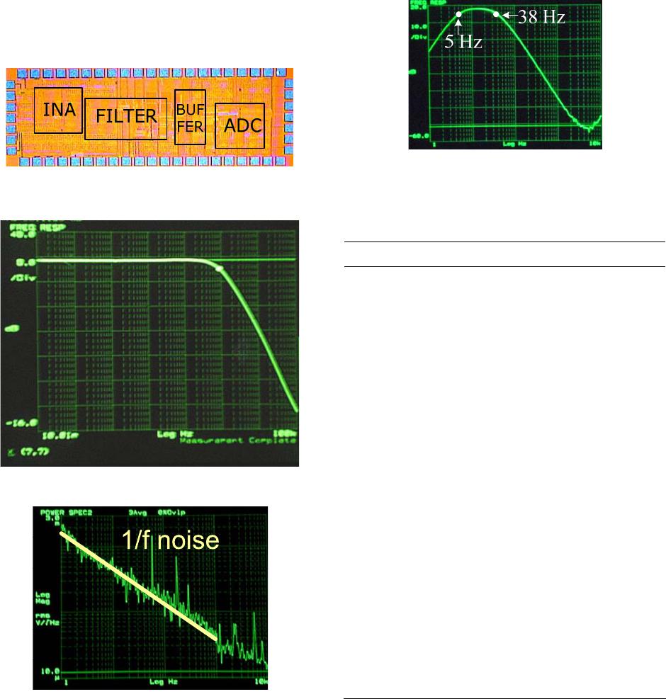
loss in the filter design. In the proposed low-frequency
filter for the AC-path, the intrinsic loss is the most im-
portant one and equals to 1.4 dB in the SPICE simula-
tion.
The comparison with other AFE ICs in the literature is
listed in Table 2. Ref. [3] accomplishes the lowest power
consumption among the AFEs for the ECG recording.
However, in that work its filter is 1st-order and embedded
within the INA, and it may be difficult to achieve high-
order accurate cut-off frequency. In contrast, in our pro-
posed method a 4th-order band pass on-chip filter is used
for the AC-path, whose current consumption of 0.62 µA
is a partial reason why the proposed AFE IC power con-
sumption is somewhat larger (in the DC-path, only the
first 1st-order filter is used.) Ref. [5] achieves good per-
formances but at the cost of very high current consump-
tion. Ref. [12] uses extensively current-mode circuits to
implement the log-domain amplifier and the log-domain
filter. Its ADC is an 8-bit sigma-delta ADC, but the
power hungry decimation filter of the ADC was not inte-
grated on-chip so the actually current consumption in the
case of Ref. [12] would be much higher. Our measured
noise performance in this AFE IC channel is on the
higher side as suggested from the SPICE simulation as
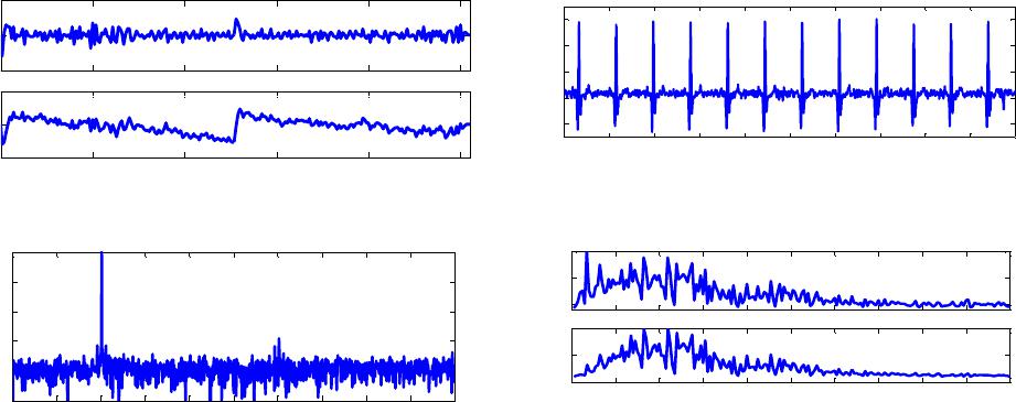
well, but it is demonstrated to still be able to provide
good ECG/EGM waveforms for heartbeat detection from
both measurement and simulation (i.e., Figures 14 and
15). Our ADC also shows excellent low power consump-
tion vs. all the other work surveyed here.
To summarize, the motivation of this proposed re-
search is to try to design a very low-power and generic
AFE IC for bio-sensing applications (say, for both wear-
able and implantable biosensors). The AFE IC can be
switched periodically to check the contact resistance and
the DC offset voltages of each electrode for continuous
Table 2. Literature comparison with other AFE ICs for
CG.
(Meas.) (Meas.) (Meas.) (Meas
E
This work* [3] [5] [12]**
.)
V DD 2 1 1 2
Techµm) 0. 0. 0. 0.
24 3
IRNHz
( (
AD s)
nology (35351835
Current (µA) 2.37 0.895 79.6 1.45**
Gain (dB) 0 - 92 5.6 - 602.8 - 5835 - 62
~0.1 - 500
(µVrms) 40 2.5
N/A
19 nV/Hz)
N/A
22 pArms)
CMRR (dB) 74 71.2 N/A N/A
C ENOB (bit7.4 10.2 > 9 ~8
ADC power (µW) 0.09 0.23 17.6 1.09
*Excluding the VREF/
consumption in the AD
2 p circhip;uding
Cation f
C uses a variable-gain DC-coupled
unding support from the
REFERENCES
[1] L. S. Y. Won. Edvinsson, D. H.
bias setu
decim
uit off-c
ilters.
**Exclthe current
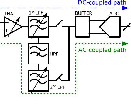
monitoring, with the selectable filtering entirely inte-
grated on-chip. Even though two paths (AC and DC
paths) have been basically implemented in parallel using
somewhat standard circuits on-chip, we have shown that
the proposed AFE IC architecture in Figure 2 is valid,
and that it can deliver comparable performance as other
designs that only use AC-coupled paths, where useful
DC info is lost and some of them also require large off-
chip HPFs. Further AFE IC design improvement to re-
move the external buffer and with improved noise per-
formance using chopper-stabilized INA will be reported
later when data becomes available.
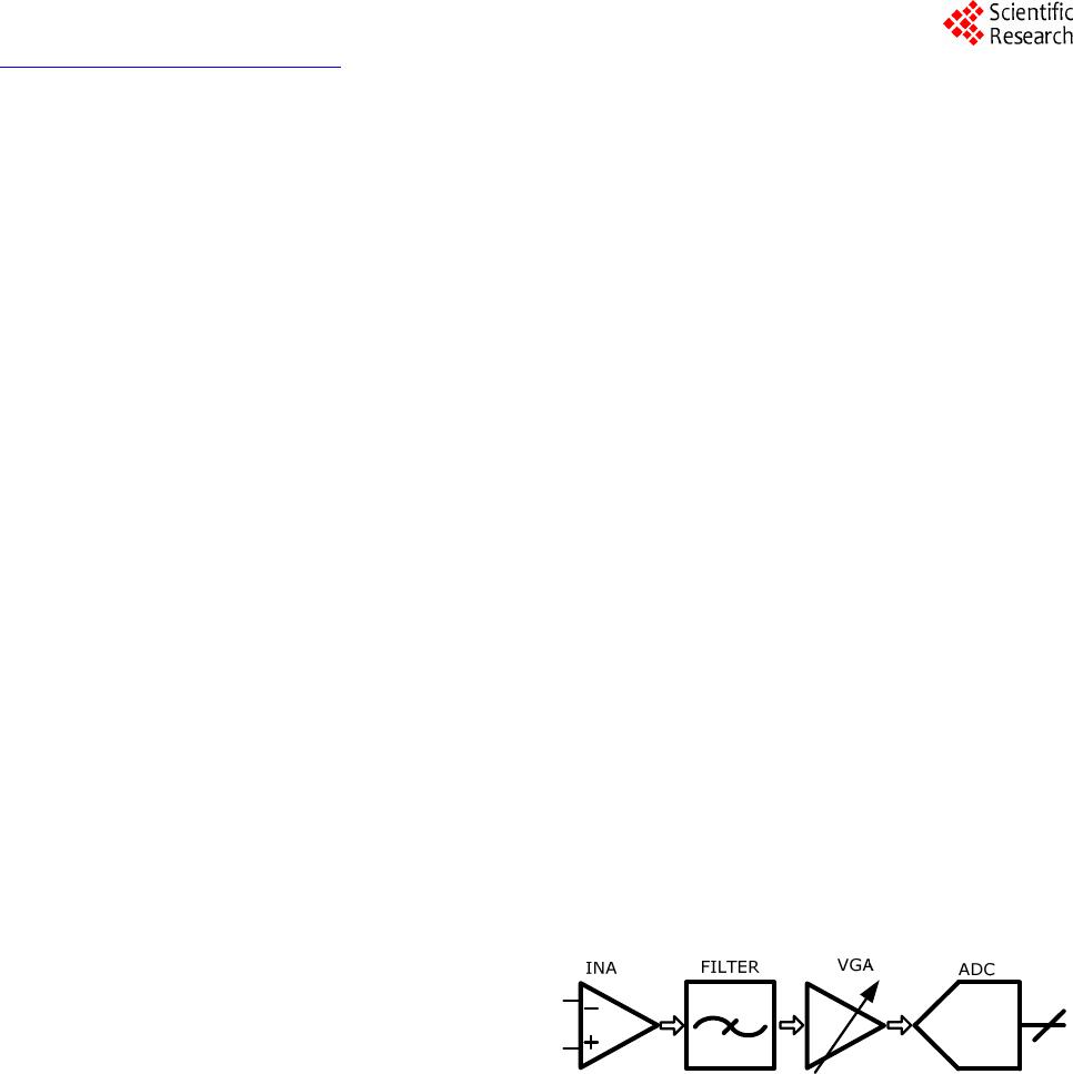
5. Conclusion
The proposed AFE I
INA, and a HPF is placed in the middle of the entire AFE
IC. This arrangement enables the AFE IC to have dual
DC/AC-coupled paths to process bio-signals with either
useful or undesired DC components. The DC-coupled
INA is designed using a DDA with a resistor feedback.
Other blocks, including variable-gain and tunable-band-
width RC filters and the ADC are also explained. Ex-
cluding the external buffer needed to properly drive the
ADC for this AFE IC, the entire AFE IC consumes only
2.37 µA/channel. The AFE IC successfully displays the
sensed ECG waveforms for clear QRS peak detection
and also exhibits correct frequency content of EGM,
suggesting that it should be adequate for peak detection
in pacemaker/ICD applications as well.
6. Acknowledgements
We are also indebted to the f
Semiconductor Research Corp. (SRC) through the Texas
Analog Center of Excellence (TxACE).
g, S. Hossain, A. Ta, J
Rivas and H. Naas, “A Very Low-Power CMOS Mixed-
Signal IC for Implantable Pacemaker Applications,” IEEE
Journal of Solid-State Circuits, Vol. 39, No. 12, 2004, pp.
2446-2456. http://dx.doi.org/10.1109/JSSC.2004.837027
[2] W. Hu, T. Nguyen, Y.-T. Liu and D.Y.C. Lie, “Ultralow
Power Analog Front-End Circuits and System Design for
an Implantable Cardioverter Defibrillator,” Proceedings
of the IEEE-NIH Life Science Systems and Application
Workshop, 2011, pp. 34-37.
[3] X. D. Zou, X. Y. Xu, L. B. Yao and Y. Lian, “A 1-V
450-nW Fully Integrated Programmable Biomedical Sen-
sor Interface System,” IEEE Journal of Solid-State Cir-
cuits, Vol. 44, No. 4, 2009, pp. 1067-1077.
http://dx.doi.org/10.1109/JSSC.2009.2014707
[4] N. Verma, A. Shoeb, J. Bohorquez, J. Dawson, J. Guttag
and A. P. Chandrakasan, “A Micro-Power EEG Acquisi-
tion SoC with Integrated Feature Extraction Processor for
Open Access OJAB
D. Y. C. LIE ET AL.
Open Access OJAB
111
a Chronic Seizure Detection System,” IEEE Journal of
Solid-State Circuits, Vol. 45, No. 4, 2010, pp. 804-816.
http://dx.doi.org/10.1109/JSSC.2010.2042245
[5] X. Liu, Y. Zheng, M. W. Phyu, F. N. Endru, V. Nava-
neethan and B. Zhao, “An Ultra-Low Power EC
G Acqui-
sition and Monitoring ASIC System for WBAN Applica-
tion,” IEEE Journal of Emerging and Selected Topics in
Circuits and System, Vol. 2, No. 1, 2012, pp. 60-70.
http://dx.doi.org/10.1109/JETCAS.2012.2187707
[6] R. Harrison and C. Charles, “A Low-Power Low-N
CMOS Amplifier for Neural Recording Applic
oise
ations,”
IEEE Journal of Solid-State Circuits, Vol. 38, No. 6, 2003,
pp. 958-965. http://dx.doi.org/10.1109/JSSC.2003.811979
[7] www.ti.com/product/ADS1291
hl, “A Versatile Building [8] E. Sackinger and W. Guggenbu
Block: The CMOS Differential Difference Amplifier,”
d G. C. Temes, “Understanding Delta-Sig-
D. Y. C. Lie and B. P. Ginsburg, “An
t.org/physiobank/database/iafdb
ully Inte-
IEEE Journal of Solid-State Circuits, Vol. 22, No. 2, 1987,
pp. 287-294.
[9] R. Schreier an
ma Data Converters”, 1st Edition, IEEE Press, New Jer-
sey, 2007.
[10] W. Hu, Y.-T. Liu,
8-Bit Single-Ended Ultra-Low-Power SAR ADC with
Novel DAC Switching and Digital Control Circuits for
Bio-Medical Applications’,” IEEE Transactions on Cir-
cuits and Systems-I (TCAS-I), Vol. 60, No. 7, 2013, pp.
1726-1739.
[11] www.physione
[12] A. Gerosa, A. Maniero and A. Neviani, “A F
grated Two-Channel A/D Interface for the Acquisition of
Cardiac Signals in Implantable Pacemakers,” IEEE Jour-
nal of Solid-State Circuit s, Vol. 39, No. 7, 2004, pp. 1083-
1093. http://dx.doi.org/10.1109/JSSC.2004.829921