Paper Menu >>
Journal Menu >>
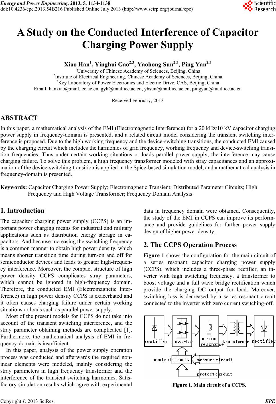 Energy and Power Engineering, 2013, 5, 1134-1138 doi:10.4236/epe.2013.54B216 Published Online July 2013 (http://www.scirp.org/journal/epe) A Study on the Conducted Interference of Capacitor Charging Power Supply Xiao Han1, Yinghui Gao2,3, Yaohong Sun2,3, Ping Yan2,3 1University of Chinese Academy of Sciences, Beijing, China 2Institute of Electrical Engineering, Chinese Academy of Sciences, Beijing, China 3Key Laboratory of Power Electronics and Electric Drive, CAS, Beijing, China Email: hanxiao@mail.iee.ac.cn, gyh@mail.iee.ac.cn, yhsun@mail.iee.ac.cn, pingyan@mail.iee.ac.cn Received February, 2013 ABSTRACT In this paper, a mathematical analysis of the EMI (Electromagnetic Interference) for a 20 kHz/10 kV capacitor charging power supply in frequency-domain is presented, and a related circuit model considering the transient switching inter- ference is proposed. Due to the high working frequency and the device-switching transitions, the conducted EMI caused by the charging circuit which includes the harmonics of grid frequency, working frequency and device-switching transi- tion frequencies. Thus under certain working situations or loads parallel power supply, the interference may cause charging failure. To solve this problem, a high frequency transformer modeled with stray capacitances and an approxi- mation of the device-switching transition is applied in the Spice-based simulation model, and a mathematical analysis in frequency-domain is presented. Keywords: Capacitor Charging Power Supply; Electromagnetic Transient; Distributed Parameter Circuits; High Frequency and High Voltage Transformer; Frequency Domain Analysis 1. Introduction The capacitor charging power supply (CCPS) is an im- portant power charging means for industrial and military applications such as distribution energy storage in ca- pacitors. And because increasing the switching frequency is a common manner to obtain high power density, which means shorter transition time during turn-on and off for semiconductor devices and leads to greater high-frequen- cy interference. Moreover, the compact structure of high power density CCPS complicates stray parameters, which cannot be ignored in high-frequency domain. Therefore, the conducted EMI (Electromagnetic Inter- ference) in high power density CCPS is exacerbated and it often causes charging failure under certain working situations or loads such as parallel power supply. Most of the present models for CCPS do not take into account of the transient switching interference, and the stray parameter obtaining methods are complicated [1]. Furthermore, the mathematical analysis of EMI in fre- quency-domain is insufficient. In this paper, analysis of the power supply operation process was conducted and afterwards the required non- inear elements were modeled, mainly considering the stray parameters in high frequency transformer and the interference of the transient switching harmonics. Satis- factory simulation results which agree with experimental data in frequency domain were obtained. Consequently, the study of the EMI in CCPS can improve its perform- ance and provide guidelines for further power supply design of higher power density. 2. The CCPS Operation Process Figure 1 shows the configuration for the main circuit of a series resonant capacitor charging power supply (CCPS), which includes a three-phase rectifier, an in- verter with high switching frequency, a transformer to boost voltage and a full wave bridge rectification which provide the charging DC output for load. Moreover, switching loss is decreased by a series resonant circuit connected to the inverter with zero current switching-off. Figure 1. Main circuit of a CCPS. Copyright © 2013 SciRes. EPE 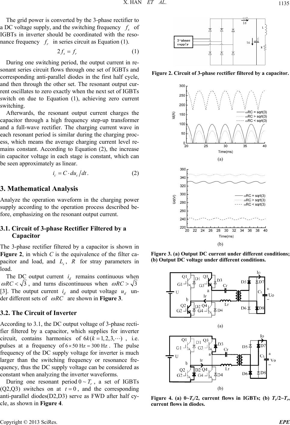 X. HAN ET AL. 1135 The grid power is converted by the 3-phase rectifier to a DC voltage supply, and the switching frequency s f of IGBTs in inverter should be coordinated with the reso- nance frequency r f in series circuit as Equation (1). 2 s r f f (1) During one switching period, the output current in re- sonant series circuit flows through one set of IGBTs and corresponding anti-parallel diodes in the first half cycle, and then through the other set. The resonant output cur- rent oscillates to zero exactly when the next set of IGBTs switch on due to Equation (1), achieving zero current switching. Afterwards, the resonant output current charges the capacitor through a high frequency step-up transformer and a full-wave rectifier. The charging current wave in each resonant period is similar during the charging proc- ess, which means the average charging current level re- mains constant. According to Equation (2), the increase in capacitor voltage in each stage is constant, which can be seen approximately as linear. . cc iC dudt (2) 3. Mathematical Analysis Analyze the operation waveform in the charging power supply according to the operation process described be- fore, emphasizing on the resonant output current. 3.1. Circuit of 3-phase Rectifier Filtered by a Capacitor The 3-phase rectifier filtered by a capacitor is shown in Figure 2, in which C is the equivalence of the filter ca- pacitor and load, and s L, for stray parameters in load. R The DC output current d remains continuous when i 3RC , and turns discontinuous when 3RC [3]. The output current d and output voltage un- der different sets of id u RC are shown in Figure 3. 3.2. The Circuit of Inverter According to 3.1, the DC output voltage of 3-phase recti- fier filtered by a capacitor, which supplies for inverter circuit, contains harmonics of, i.e. pulses at a frequency of. The pulse frequency of the DC supply voltage for inverter is much larger than the switching frequency or resonance fre- quency, thus the DC supply voltage can be considered as constant when analyzing the inverter waveforms. 6(1,2,3, )kk Hz300 Hz6 50 During one resonant period, a set of IGBTs (Q2,Q3) switches on at , and the corresponding anti-parallel diodes(D2,D3) serve as FWD after half cy- cle, as shown in Figure 4. 0~ r T 0t Figure 2. Circuit of 3-phase rectifier filtered by a capacitor. (a) (b) Figure 3. (a) Output DC current under different conditions; (b) Output DC voltage under different conditions. (a) (b) Figure 4. (a) 0~Tr/2, current flows in IGBTs; (b) Tr/2~Tr, current flows in diodes. Copyright © 2013 SciRes. EPE 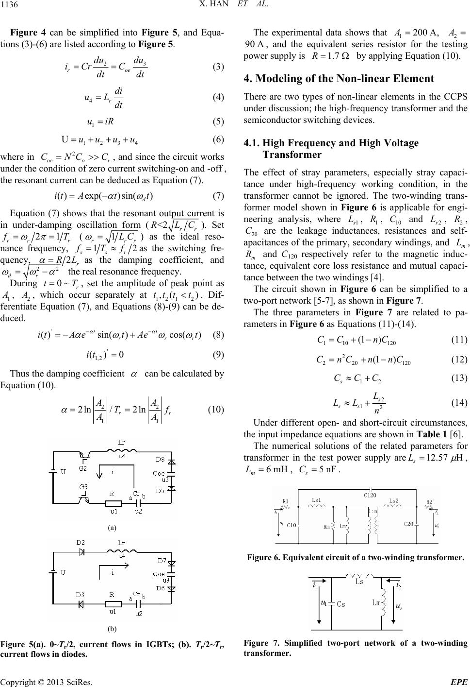 X. HAN ET AL. 1136 Figure 4 can be simplified into Figure 5, and Equa- tions (3)-(6) are listed according to Figure 5. 3 2 r du du iCr C dt dt o e (3) 4rdi uL dt (4) 1 uiR (5) 123 Uuuuu 2 4 (6) where in oe or , and since the circuit works under the condition of zero current switching-on and -off , the resonant current can be deduced as Equation (7). CNCC ()exp()sin() d it Att (7) Equation (7) shows that the resonant output current is in under-damping oscillation form (<2 rr RLC). Set 21 rr r f T (1 rr LC r ) as the ideal reso- nance frequency, 1 ssr 2 f Tf as the switching fre- quency, 2r RL as the damping coefficient, and 22 dr the real resonance frequency. During , set the amplitude of peak point as 1 0~ r tT A , 2 A , which occur separately a2 ). Dif- ferentiate Equation (7), and Equations (8)-(9) can be de- duced. t r 121 ,(ttt t ' ()sin()cos() tt rr itA etAet (8) ' 1,2 () 0it (9) Thus the damping coefficient can be calculated by Equation (10). 2 11 2ln /2ln r A T AA 2 r A f (10) (a) (b) Figure 5(a). 0~Tr/2, current flows in IGBTs; (b). Tr/2~Tr, current flows in diodes. The experimental data shows that 1 2 200 A,A A , and the equivalent series resistor for the testing power supply is 90 A 1.7R by applying Equation (10). 4. Modeling of the Non-linear Element There are two types of non-linear elements in the CCPS under discussion; the high-frequency transformer and the semiconductor switching devices. 4.1. High Frequency and High Voltage Transformer The effect of stray parameters, especially stray capaci- tance under high-frequency working condition, in the transformer cannot be ignored. The two-winding trans- former model shown in Figure 6 is applicable for engi- neering analysis, where 1 s L, 1, 10 and 2 R C s L, 2, 20 are the leakage inductances, resistances and self- apacitances of the primary, secondary windings, and m, m and C120 respectively refer to the magnetic induc- tance, equivalent core loss resistance and mutual capaci- tance between the two windings [4]. R L C R The circuit shown in Figure 6 can be simplified to a two-port network [5-7], as shown in Figure 7. The three parameters in Figure 7 are related to pa- rameters in Figure 6 as Equations (11)-(14). 110 12 (1 )CCnC 0 (11) 2 2 20120 (1 )CnCnnC (12) 1s CCC 2 (13) 2 12 s ss L LL n (14) Under different open- and short-circuit circumstances, the input impedance equations are shown in Table 1 [6]. The numerical solutions of the related parameters for transformer in the test power supply are12.57 s L , 6mΗ m L , 5nF s C . Figure 6. Equivalent circuit of a two-winding transformer. Figure 7. Simplified two-port network of a two-winding transformer. Copyright © 2013 SciRes. EPE 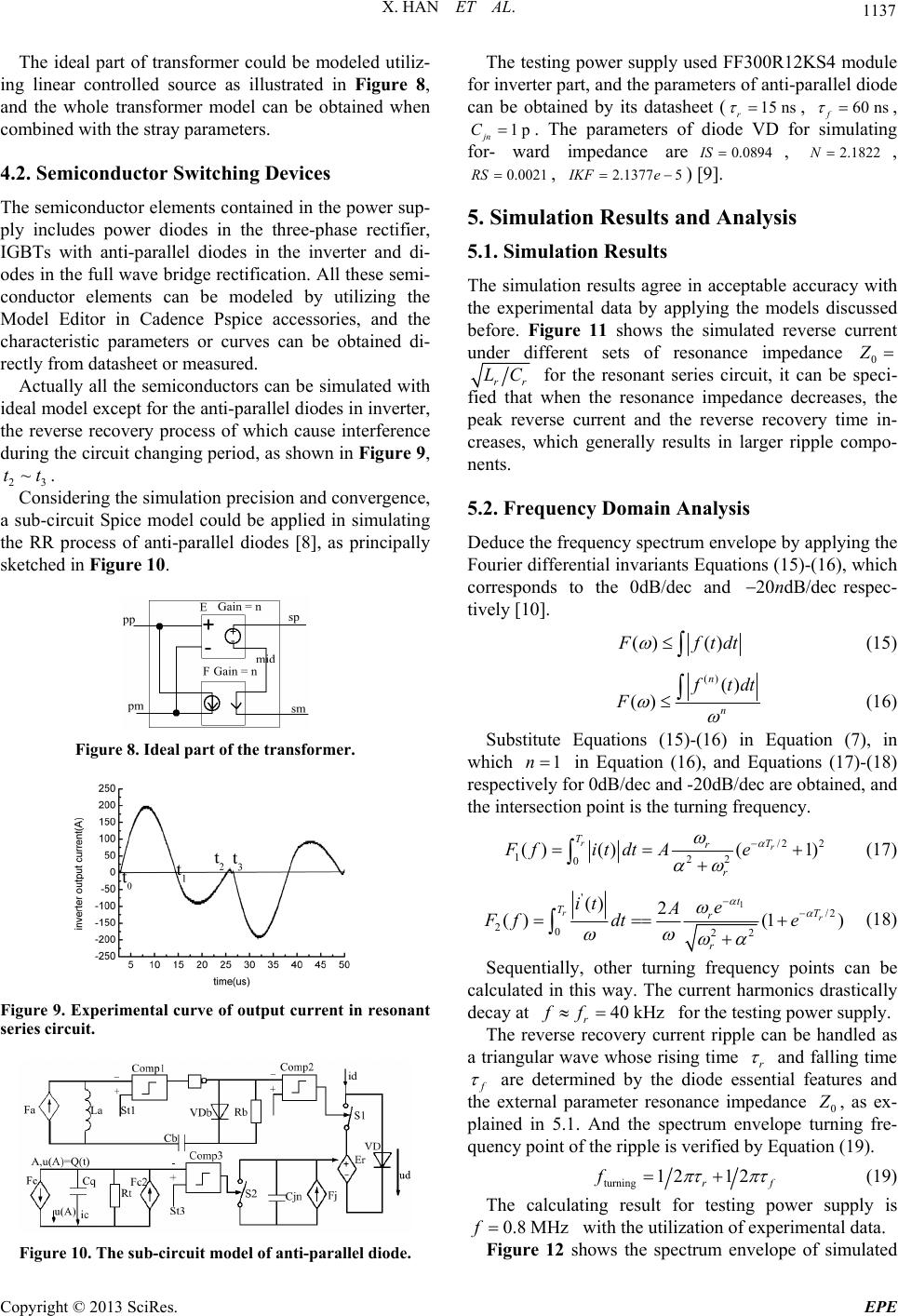 X. HAN ET AL. 1137 The ideal part of transformer could be modeled utiliz- ing linear controlled source as illustrated in Figure 8, and the whole transformer model can be obtained when combined with the stray parameters. 4.2. Semiconductor Switching Devices The semiconductor elements contained in the power sup- ply includes power diodes in the three-phase rectifier, IGBTs with anti-parallel diodes in the inverter and di- odes in the full wave bridge rectification. All these semi- conductor elements can be modeled by utilizing the Model Editor in Cadence Pspice accessories, and the characteristic parameters or curves can be obtained di- rectly from datasheet or measured. Actually all the semiconductors can be simulated with ideal model except for the anti-parallel diodes in inverter, the reverse recovery process of which cause interference during the circuit changing period, as shown in Figure 9, . 23 ~tt Considering the simulation precision and convergence, a sub-circuit Spice model could be applied in simulating the RR process of anti-parallel diodes [8], as principally sketched in Figure 10. Figure 8. Ideal part of the transformer. Figure 9. Experimental curve of output current in resonant series circu it. Figure 10. The sub-circuit model of anti-parallel diode. The testing power supply used FF300R12KS4 module for inverter part, and the parameters of anti-parallel diode can be obtained by its datasheet (, , . The parameters of diode VD for simulating for- ward impedance are, 15 ns r 0.0894 60 ns f 2.1822N 1p jn C IS , 0.0021RS , 2.1377 5IKF e ) [9]. 5. Simulation Results and Analysis 5.1. Simulation Results The simulation results agree in acceptable accuracy with the experimental data by applying the models discussed before. Figure 11 shows the simulated reverse current under different sets of resonance impedance 0 Z rr LC for the resonant series circuit, it can be speci- fied that when the resonance impedance decreases, the peak reverse current and the reverse recovery time in- creases, which generally results in larger ripple compo- nents. 5.2. Frequency Domain Analysis Deduce the frequency spectrum envelope by applying the Fourier differential invariants Equations (15)-(16), which corresponds to the 0dB/dec and respec- tively [10]. 20 dB/decn () () F ftdt (15) () () () n n f tdt F (16) Substitute Equations (15)-(16) in Equation (7), in which 1n in Equation (16), and Equations (17)-(18) respectively for 0dB/dec and -20dB/dec are obtained, and the intersection point is the turning frequency. /2 2 122 0 () ()(1) rr TT r r Ffitdt Ae (17) 1 ' /2 2022 () 2 ()(1 ) rr t TT r r it e A Ff dte (18) Sequentially, other turning frequency points can be calculated in this way. The current harmonics drastically decay at 40 kHz r ff for the testing power supply. The reverse recovery current ripple can be handled as a triangular wave whose rising time r and falling time f are determined by the diode essential features and the external parameter resonance impedance 0 Z , as ex- plained in 5.1. And the spectrum envelope turning fre- quency point of the ripple is verified by Equation (19). turning 12 12 r ff (19) The calculating result for testing power supply is 0.8 MHzf with the utilization of experimental data. Figure 12 shows the spectrum envelope of simulated Copyright © 2013 SciRes. EPE 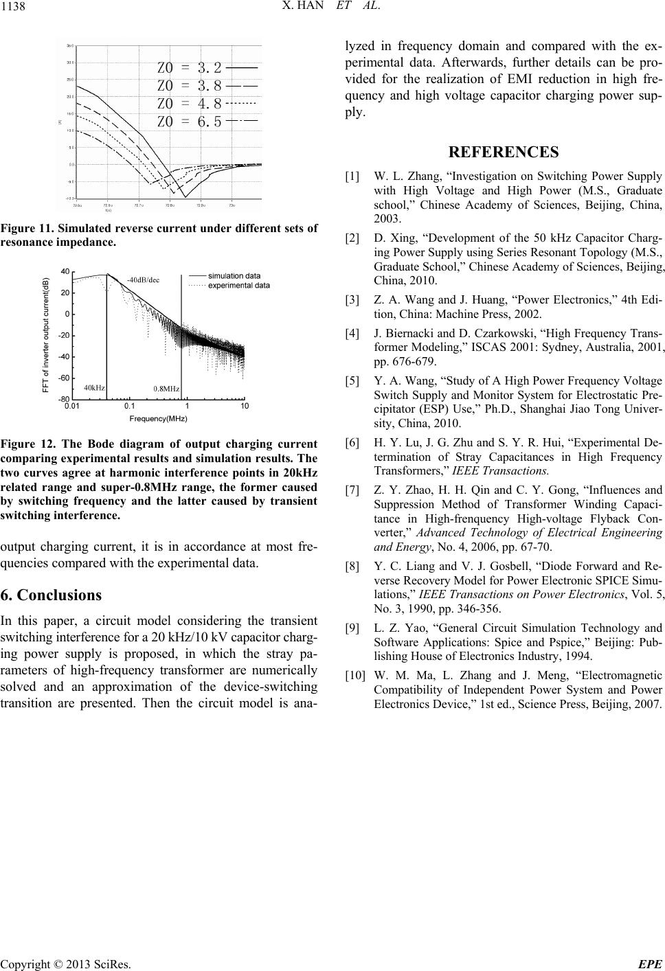 X. HAN ET AL. Copyright © 2013 SciRes. EPE 1138 Figure 11. Simulated reverse current under different sets of resonance impedance. Figure 12. The Bode diagram of output charging current comparing experimental results and simulation results. The two curves agree at harmonic interference points in 20kHz related range and super-0.8MHz range, the former caused by switching frequency and the latter caused by transient switching interference. output charging current, it is in accordance at most fre- quencies compared with the experimental data. 6. Conclusions In this paper, a circuit model considering the transient switching interference for a 20 kHz/10 kV capacitor charg- ing power supply is proposed, in which the stray pa- rameters of high-frequency transformer are numerically solved and an approximation of the device-switching transition are presented. Then the circuit model is ana- lyzed in frequency domain and compared with the ex- perimental data. Afterwards, further details can be pro- vided for the realization of EMI reduction in high fre- quency and high voltage capacitor charging power sup- ply. REFERENCES [1] W. L. Zhang, “Investigation on Switching Power Supply with High Voltage and High Power (M.S., Graduate school,” Chinese Academy of Sciences, Beijing, China, 2003. [2] D. Xing, “Development of the 50 kHz Capacitor Charg- ing Power Supply using Series Resonant Topology (M.S., Graduate School,” Chinese Academy of Sciences, Beijing, China, 2010. [3] Z. A. Wang and J. Huang, “Power Electronics,” 4th Edi- tion, China: Machine Press, 2002. [4] J. Biernacki and D. Czarkowski, “High Frequency Trans- former Modeling,” ISCAS 2001: Sydney, Australia, 2001, pp. 676-679. [5] Y. A. Wang, “Study of A High Power Frequency Voltage Switch Supply and Monitor System for Electrostatic Pre- cipitator (ESP) Use,” Ph.D., Shanghai Jiao Tong Univer- sity, China, 2010. [6] H. Y. Lu, J. G. Zhu and S. Y. R. Hui, “Experimental De- termination of Stray Capacitances in High Frequency Transformers,” IEEE Transactions. [7] Z. Y. Zhao, H. H. Qin and C. Y. Gong, “Influences and Suppression Method of Transformer Winding Capaci- tance in High-frenquency High-voltage Flyback Con- verter,” Advanced Technology of Electrical Engineering and Energy, No. 4, 2006, pp. 67-70. [8] Y. C. Liang and V. J. Gosbell, “Diode Forward and Re- verse Recovery Model for Power Electronic SPICE Simu- lations,” IEEE Transactions on Power Electronics, Vol. 5, No. 3, 1990, pp. 346-356. [9] L. Z. Yao, “General Circuit Simulation Technology and Software Applications: Spice and Pspice,” Beijing: Pub- lishing House of Electronics Industry, 1994. [10] W. M. Ma, L. Zhang and J. Meng, “Electromagnetic Compatibility of Independent Power System and Power Electronics Device,” 1st ed., Science Press, Beijing, 2007. |