Energy and Power Engineering, 2013, 5, 1069-1071
doi:10.4236/epe.2013.54B203 Published Online July 2013 (http://www.scirp.org/journal/epe)
Analysis of Output Characteristics of Buck Converter
Jinquan Wang, Qian Li, Pengchao Song, Pengfei Hou
Engineering Institute of Defence, PLA University of Science&Technology, Nanjing, China
Email: lqtx_0@qq.com
Received February, 2013
ABSTRACT
This Article introduced the concept, topology and function of voltage type Buck converter, built a small signal model,
analysis the negative impedance character of converter, then simulated a Buck-type DC/ DC through MATLAB, ob-
served the dynamic response of converter to pulse-type power load, verified the small-signal theoretical by simulation,
lay the foundation for analyzing DC system stability.
Keywords: Small-signal Model; Nput Impedance; Buck Converter; DC System
1. Introduction
With the rapid development of power electronics tech-
nology and electricity, the number of electronic devices
has more and more extensive application in the grid.
Such a wide range of applications also causing a series of
bad effects, For example, switching tube frequent break-
ing reduces the energy utilization efficiency and lifetime
of the device, the improper design of the internal pa-
rameters of the commutation device will also bring a lot
of problem such as convergence and stability of the sys-
tem[1-3]; Furthermore, the power electronic devices as a
non-linear load inject to grid, resulting in a large number
of harmonics current, which brings a lot of security
problems caused by heat stress. Traditional linear load
statistics matching criteria in this environment has been
challenged. Unstability caused by this power mismatch is
also the key issue of smart micro-grid system, which
consists of source converter output impedance and the
input impedance of the load converter joint decision, in
order to a more convenience study, there need establish
an approximate mathematical model[2,4,5], taking into
account the constant power characteristics of the Buck
converter, there is a negative input impedance character-
istics, according to a given Buck converter, change its
load characteristics, and then separately to analyze the
change in the impedance of the converter. Now study on
DC/DC converter’s negative impedance is mainly con-
centrated in the topology, internal parameters and control
model, in this paper, change the output power to research
Buck circuit input impedance characteristics.
2. Design and Analysis of Voltage type Buck
Converter
2.1. Analysis of Voltage Type Buck
The Buck Chopper is the most widely used form of a
circuit in the DC chopper circuit. Buck circuit is used to
reducing the voltage of the DC power supply, it uses
full-controlled device to control the DC source such of
IGBT, MOSFET and so on, when closed, the DC power
supply to the load, When turned off, the inductor has
been charged still conduct through diode, supply power
to load, so as to achieve the purpose of the step-down
chopper. Having inferred to the following formulation:
o
EDU
(1)
Einput DC voltage
Dduty
Uooutput voltage
In order to stabilize and adjust the output voltage of
the DC/DC converter, generally, use the voltage or cur-
rent- control mode to adjust the duty cycle, as shown in
Figures 1 and 2. Advantages of current mode control:
faster transient response and improve the stability of the
output voltage accuracy, and has current limiting func-
tion by itself, easy-to-achieve converter overcurrent pro-
tection, and thus easier for multiple power supplies in
parallel achieve both streams. Voltage mode control: the
advantages of detecting only one variable output voltage,
and only one control loop, relatively simple to design and
analysis; due to the large amplitude of the serrasoid
waveform, having the strong anti-jamming capability.
This article only analysis the Voltage type Buck con-
verter.
Uin
S
+
-Iref
Uo
e
L
iLi
PWM
VD
A
Figure 1. Current type Buck converter.
Copyright © 2013 SciRes. EPE
J. Q. WANG ET AL.
1070
Figure 2 .Voltage type Buck converter.
For a more intuitive understanding of the negative im-
pedance characteristics of the Buck converter, we assume
that the BUCK circuit components are ideal, the power
transfer efficiency of 100%, the converter has been at the
CCM model. The converters simulation can infer that
inductance is smaller, the greater the overshoot, more
stable; capacitance is smaller, smaller overshoot, the
greater the ripple. Therefore there is need to calculate the
appropriate filter capacitors, inductors which can meet
the requirements of the simulation waveform.
2.2. Small Signal Model
The main course to analysis DC power converter is state
space averaging method [6], given the coefficient matrix
of the equation of state A1, b1, A2, b2, C1
T, C2
T under two
switching state, can infer the mathematical expressions
that describe the steady-state and dynamic small signal
characteristics, induce to the low-frequency equivalent
mode, then through to the disturbance, linearization and
other steps, can get low-frequency small-signal behavior
equation:
^
^^
12 12
[()() ]
ss
dx ^
A
xbvAAXb bVd
dt   (2)
^^
12
()
TTT
yCxC CXd
^
(3)
By the formula (2) and (3) dynamic low-frequency re-
sponse can be obtained by the Laplace transform of the
small signal characteristics, such as the output of the in-
put to the conduction ratio control transfer function. De-
duced from the voltage on the conduction the transfer
function Gvd ratio control is as follows:
^
^
1
12 12
^
()0
12
() ()[( )()
()
()
T]
s
vs
TT
ys CsIAA AXbbV
ds
CCX
 

(4)
Transfer function can be obtained from the above equ-
ation:
0
22
111 1
11
vd s
V
GV
SL
CL D
SCLS
RC LCR

 
S
(5)
3. Analysis and Simulation
For deep understanding of the closed-loop input imped-
ance characteristics of the converter, establish volt-
age-mode control of the synchronous rectifier BUCK
converter model [7-9] and simulation, as shown in Fig-
ure 3;assuming the efficiency of the inverter is 100%:
0in in
PUI
(6)
In formula Uin and Iin is input voltage and input current.
Small signal perturbations superimposed on the amount
of the steady state in the above formula, get following
formula:
^^
0
0()(
inin in in
PPUuI i 
^
)
^
(7)
Assuming the converter's output power is constant,
that is to ignore the disturbance of the output power:
^^^
0in inininininin in
PUI UiIuui (8)
According to formula (6),then ignores the second or-
der component:
^2
^
0
in in
ic
in
uU
ZP
i
 (9)
The formula (9) explaining the reasons for a
closed-loop input impedance appears the negative resis-
tance characteristic. Absolute of input impedance de-
pending on the size of the input voltage and output power,
make input voltage constant, the converter’s input cur-
rent will be reduced when increasing the output power of
the converter, and verify by simulation following.
Figure 3. Buck converter small signal model.
Copyright © 2013 SciRes. EPE
J. Q. WANG ET AL.
Copyright © 2013 SciRes. EPE
1071
Figure 4. Simulation model.
Figure 5. Current waveform.
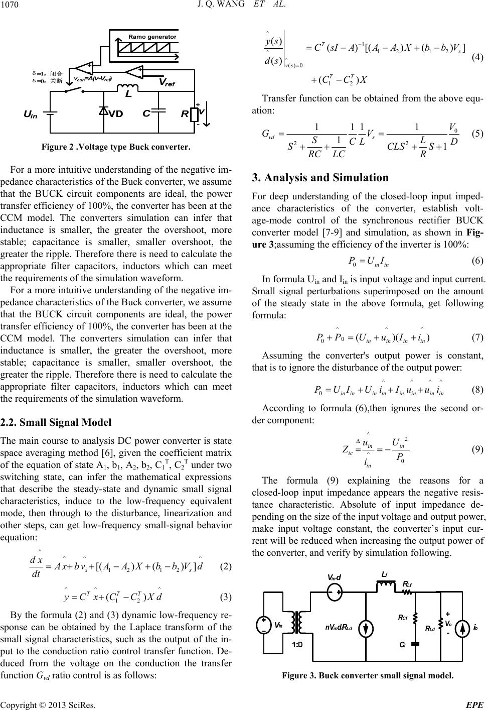
In Buck converter simulation, set the voltage feedback
loop control system, the converter input voltage E = 200
V, output voltage Uo = 120 V, the initial resistive load is
1.5 , due to it is assumed that the converter has been
working in CCM state[10-12], according to inductance
LC of formula, it can obtain the value of the L, C, and
then multiplied by a certain margin coefficient, and fi-
nally set L = 6e-5 H, C = 5e-4F,make simulation time is
0.02 seconds, and paralle a plurality of resistive load in
the load terminal, then trigger pulse at different times, the
purpose of increasing the load is to observe the change of
the input current, and the validation of the negative im-
pedance characteristics. The simulation model is shown
in Figure 4.
4. Results of Simulation
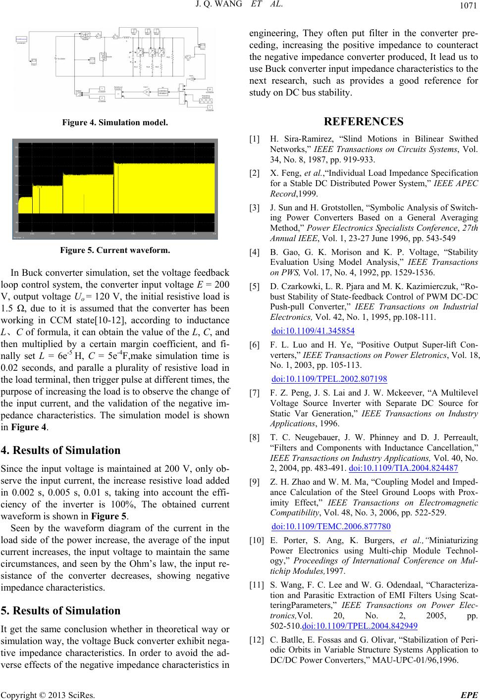
Since the input voltage is maintained at 200 V, only ob-
serve the input current, the increase resistive load added
in 0.002 s, 0.005 s, 0.01 s, taking into account the effi-
ciency of the inverter is 100%, The obtained current
waveform is shown in Figure 5.
Seen by the waveform diagram of the current in the
load side of the power increase, the average of the input
current increases, the input voltage to maintain the same
circumstances, and seen by the Ohm’s law, the input re-
sistance of the converter decreases, showing negative
impedance characteristics.
5. Results of Simulation
It get the same conclusion whether in theoretical way or
simulation way, the voltage Buck converter exhibit nega-
tive impedance characteristics. In order to avoid the ad-
erse effects of the negative impedance characteristics in
engineering, They often put filter in the converter pre-
ceding, increasing the positive impedance to counteract
the negative impedance converter produced, It lead us to
use Buck converter input impedance characteristics to the
next research, such as provides a good reference for
study on DC bus stability.
REFERENCES
[1] H. Sira-Ramirez, “Slind Motions in Bilinear Swithed
Networks,” IEEE Transactions on Circuits Systems, Vol.
34, No. 8, 1987, pp. 919-933.
[2] X. Feng, et al.,“Individual Load Impedance Specification
for a Stable DC Distributed Power System,” IEEE APEC
Record,1999.
[3] J. Sun and H. Grotstollen, “Symbolic Analysis of Switch-
ing Power Converters Based on a General Averaging
Method,” Power Electronics Specialists Conference, 27th
Annual IEEE, Vol. 1, 23-27 June 1996, pp. 543-549
[4] B. Gao, G. K. Morison and K. P. Voltage, “Stability
Evaluation Using Model Analysis,” IEEE Transactions
on PWS, Vol. 17, No. 4, 1992, pp. 1529-1536.
[5] D. Czarkowki, L. R. Pjara and M. K. Kazimierczuk, “Ro-
bust Stability of State-feedback Control of PWM DC-DC
Push-pull Converter,” IEEE Transactions on Industrial
Electronics, Vol. 42, No. 1, 1995, pp.108-111.
doi:10.1109/41.345854
[6] F. L. Luo and H. Ye, “Positive Output Super-lift Con-
verters,” IEEE Transactions on Power Eletronics, Vol. 18,
No. 1, 2003, pp. 105-113.
doi:10.1109/TPEL.2002.807198
[7] F. Z. Peng, J. S. Lai and J. W. Mckeever, “A Multilevel
Voltage Source Inverter with Separate DC Source for
Static Var Generation,” IEEE Transactions on Industry
Applications, 1996.
[8] T. C. Neugebauer, J. W. Phinney and D. J. Perreault,
“Filters and Components with Inductance Cancellation,”
IEEE Transactions on Industry Applications, Vol. 40, No.
2, 2004, pp. 483-491. doi:10.1109/TIA.2004.824487
[9] Z. H. Zhao and W. M. Ma, “Coupling Model and Imped-
ance Calculation of the Steel Ground Loops with Prox-
imity Effect,” IEEE Transactions on Electromagnetic
Compatibility, Vol. 48, No. 3, 2006, pp. 522-529.
doi:10.1109/TEMC.2006.877780
[10] E. Porter, S. Ang, K. Burgers, et al.,“Miniaturizing
Power Electronics using Multi-chip Module Technol-
ogy,” Proceedings of International Conference on Mul-
tichip Modules,1997.
[11] S. Wang, F. C. Lee and W. G. Odendaal, “Characteriza-
tion and Parasitic Extraction of EMI Filters Using Scat-
teringParameters,” IEEE Transactions on Power Elec-
tronics,Vol. 20, No. 2, 2005, pp.
502-510.doi:10.1109/TPEL.2004.842949
[12] C. Batlle, E. Fossas and G. Olivar, “Stabilization of Peri-
odic Orbits in Variable Structure Systems Application to
DC/DC Power Converters,” MAU-UPC-01/96,1996.
v