Paper Menu >>
Journal Menu >>
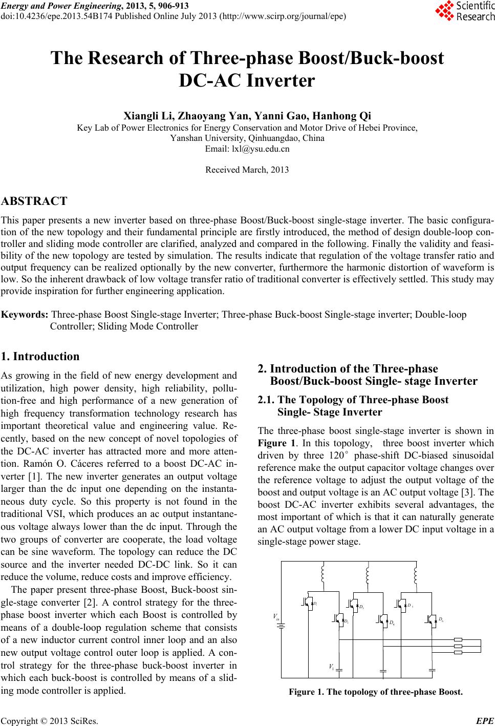 Energy and Power Engineering, 2013, 5, 906-913 doi:10.4236/epe.2013.54B174 Published Online July 2013 (http://www.scirp.org/journal/epe) The Research of Three-phase Boost/Buck-boost DC-AC Inverter Xiangli Li, Zhaoyang Yan, Yanni Gao, Hanhong Qi Key Lab of Power Electronics for Energy Conservation and Motor Drive of Hebei Province, Yanshan University, Qinhuangdao, China Email: lxl@ysu.edu.cn Received March, 2013 ABSTRACT This paper presents a new inverter based on three-phase Boost/Buck-boost single-stage inverter. The basic configura- tion of the new topology and their fundamental principle are firstly introduced, the method of design double-loop con- troller and sliding mode controller are clarified, an alyzed and compared in the following. Finally the valid ity and feasi- bility of the new topology are tested by simulation. The results indicate that regulation of the voltage transfer ratio and output frequency can be realized optionally by the new converter, furthermore the harmonic distortion of waveform is low. So the inherent drawback of low voltage transfer ratio of traditio n al conv erter is effectiv ely settled. Th is study may provide inspiration for further engineering application. Keywords: Three-phase Boost Single-stage Inverter; Three-phase Buck-boost Single-stage inverter; Double-loop Controller; Sliding Mode Controller 1. Introduction As growing in the field of new energy development and utilization, high power density, high reliability, pollu- tion-free and high performance of a new generation of high frequency transformation technology research has important theoretical value and engineering value. Re- cently, based on the new concept of novel topologies of the DC-AC inverter has attracted more and more atten- tion. Ramón O. Cáceres referred to a boost DC-AC in- verter [1]. The new inverter generates an output voltage larger than the dc input one depending on the instanta- neous duty cycle. So this property is not found in the traditional VSI, which produces an ac output instantane- ous voltage always lower than the dc input. Through the two groups of converter are cooperate, the load voltage can be sine waveform. The topology can reduce the DC source and the inverter needed DC-DC link. So it can reduce the volume, reduce costs and improve efficiency. The paper present three-phase Boost, Buck-boost sin- gle-stage converter [2]. A control strategy for the three- phase boost inverter which each Boost is controlled by means of a double-loop regulation scheme that consists of a new inductor current control inner loop and an also new output voltage control outer loop is applied. A con- trol strategy for the three-phase buck-boost inverter in which each buck-boost is controlled by means of a slid- ing mode controller is applied. 2. Introduction of the Three-phase Boost/Buck-boost Single- stage Inverter 2.1. The Topology of Three-phase Boost Single- Stage Inverter The three-phase boost single-stage inverter is shown in Figure 1. In this topology, three boost inverter which driven by three 120°phase-shift DC-biased sinusoidal reference make the output capacitor voltage changes over the reference voltage to adjust the output voltage of the boost and output voltage is an AC output voltage [3]. The boost DC-AC inverter exhibits several advantages, the most important of which is that it can naturally generate an AC output voltag e from a lower DC input vo ltage in a single-stage power stage. 1 V in V 1 D 2 D 3 D 4 D 5 D 6 D Figure 1. The topology of three-phase Boost. Copyright © 2013 SciRes. EPE 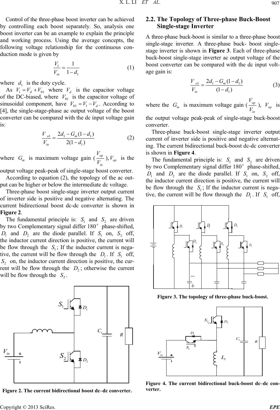 X. L. LI ET AL. 907 Control of the three-phase boost inverter can be achieved by controlling each boost separately. So, analysis one boost inverter can be an example to explain the principle and working process. Using the average concepts, the following voltage relationship for the continuous con- duction mode is given by 1 1 1 1 in V Vd (1) where is the duty cycle. 1 d As 101d where d V is the capacitor voltage of the DC-biased, where 01 is the capacitor voltage of sinusoidal component, have 011 d. According to [4], the single-stage-phase ac output voltage of the boost converter can be compared with the dc inpu t voltag e gain is: VVV VVVV 11 1 2(1 2(1 ) om in VdGd Vd 1 ) (2) where is maximum voltage gain ( m Gop in V V), is the output volta ge peak - peak of singl e-stage boost conve rt er. op V According to equation (2), the topology of the ac out- put can be higher or below the intermediate dc voltage. Three-phase boost single-stage inverter output current of inverter side is positive and negative alternating. The current bidirectional boost dc-dc converter is shown in Figure 2. The fundamental principle is: 1 and 2 are driven by two Complementary signal differ 180°phase-shifted, 1 and 2 are the diode parallel. If 1 on, 2 off, the inductor current direction is positive, the current will be flow through the 1; If the inductor current is nega- tive, the current will be flow throu gh the 1. If 1 off, 2 on, the inductor current direction is positiv e, the cur- rent will be flow through the ; otherwise the current will be flow through the . S 2 S S D D S D S S S D 2 S 1 S 1 D 2 S 2 D 1 C R in V Figure 2. The current bidirectional boost dc–dc converter. 2 A three-phase buck-bilar to a three-phase boost .2. The Topology of Three-phase Buck-Boost Single-stage Inverter oost is sim single-stage inverter. A three-phase buck- boost single- stage inverter is shown in Figure 3. Each of three-phase buck-boost single-stage inverter ac output voltage of the boost converter can be compared with the dc input volt- age gain is: 11 1 1 2(1 (1 ) om in VdGd Vd ) (3) where the is maximum voltage gain ( m G op in V V), is the output voltage peak-peak of single-stage buck-boost ase buck-boost single-stage inverter output cu inciple is: and are driven by op V converter. Three-ph rrent of inverter side is positive and negative alternat- ing. The current bidirectional buck-boost dc-dc converter is shown in Figure 4. The fundamental pr1 S er 2 S ph th two Complementary signal diff 180°ase-shifted, 1 D and 2 D are the diode parallel. If 1 S on, 2 S off, inductor current direction is positive, e curre will be flow through the 1 S; If the inductor current is nega- tive, the current will bflow through the 1 D. If 1 S off, the nt e 1 D 2 D 3 D 4 D 5 D 6 D Figure 3. The topology of three-phase buck-boost. 2 S 1 D 1 S 2 D 1 C R in V 1 L Figure 4. The current bidirectional buck-boost dc–dc con- verter. Copyright © 2013 SciRes. EPE 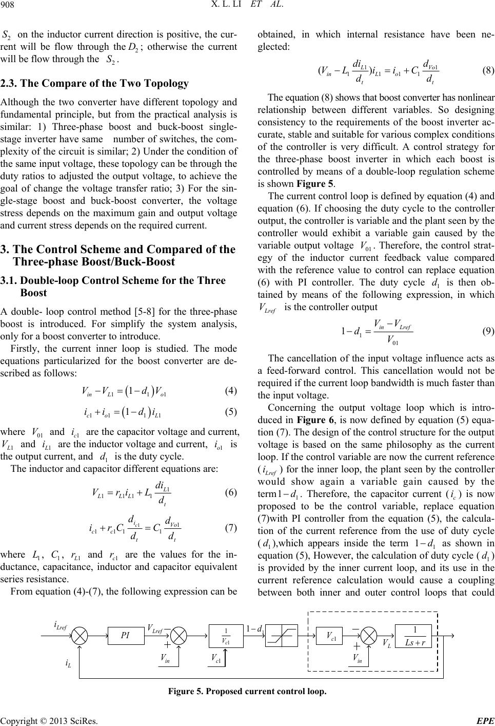 X. L. LI ET AL. Copyright © 2013 SciRes. EPE 908 he inductor current direction is positive, the cur- 2.3. The Compare of the Two Topology logy and 3.1he Three A doub control method [5-8] for the three-phase ied. The mode eq 2 S on tobtained, in which internal resistance have been ne- glected: rent will be flow through the2 D; otherwise the current will be flow through the 2 S. 1 1 1111 () Vo L inL o tt d di VLi iC dd (8) The equation (8) shows that boost converter has nonlinear relationship between different variables. So designing consistency to the requirements of the boost inverter ac- curate, stable and suitab le for various complex cond itio ns of the controller is very difficult. A control strategy for the three-phase boost inverter in which each boost is controlled by means of a double-loop regulation scheme is shown Figure 5. Although the two converter have different topo fundamental principle, but from the practical analysis is similar: 1) Three-phase boost and buck-boost single- stage inverter have same number of switches, the com- plexity of the circuit is similar; 2) Under the condition of the same input voltage, these topology can be throu gh the duty ratios to adjusted the output voltage, to achieve the goal of change the voltage transfer ratio; 3) For the sin- gle-stage boost and buck-boost converter, the voltage stress depends on the maximum gain and output voltage and current stress depends on the required current. The current control loop is defined by equation (4) and equation (6). If choosing the duty cycle to the controller output, the controller is variable and the plant seen by the controller would exhibit a variable gain caused by the variable output voltage 01 . Therefore, the control strat- egy of the inductor current feedback value compared with the reference value to control can replace equation (6) with PI controller. The duty cycle 1 is then ob- tained by means of the following expression, in which V d L ref V is the controller output 3. The Control Scheme and Compared of the Three-phase Boost/Buck-Boost . Double-loop Control Scheme for t Boost le- loop 101 1in Lref VV dV (9) boost is introduced. For simplify the system analysis, only for a boost converter to introduce. Firstly, the current inner loop is studThe cancellation of the input voltage influence acts as a feed-forward control. This cancellation would not be required if the current loop bandwidth is much faster than the input voltage. uations particularized for the boost converter are de- scribed as follows: 11 1 in Lo VV dV 1 (4) Concerning the output voltage loop which is intro- duced in Figure 6, is now defined by equation (5) equa- tion (7). The design of the control structure for the output voltage is based on the same philosophy as the current loop. If the control variable are now the current reference ( L ref i) for the inner loop, the plant seen by the controller would show again a variable gain caused by the term 1 1d . Therefore, the capacitor current (c i) is now proposed to be the control variable, replace equation (7)with PI controller from the equation (5), the calcula- tion of the current reference from the use of duty cycle (1 d),which appears inside the term 1 as shown in equation (5), However, the calculation of duty cycle (1) is provided by the inner current loop, and its use in the current reference calculation would cause a coupling between both inner and outer control loops that could 1dd 11 1 1 co L ii di 1 (5) where and are the capacitor voltage and current, 01 V1c i 1 L V an1 d L i are e inductor voltage and current, 1o i is outputrrent, and 1 d is the duty cycle. The inductor and capacitor different equation th the cus are: 1 1111 L LLL t di VriL d (6) 11 111 1 c iVo cc t dd irC C d t d (7) where 1 L, 1 C, 1 L r tan and are the values for the in- (4)-(7), the following expression can be 1c r ucductanccacice, indtor and capacitor equivalent series resistance. From equation e, pa 1c V r L s 1 L i Lref V in V 1c V 1 1d L V in V PI Lref i 1 1 c V Figure 5. Proposed current control loop. 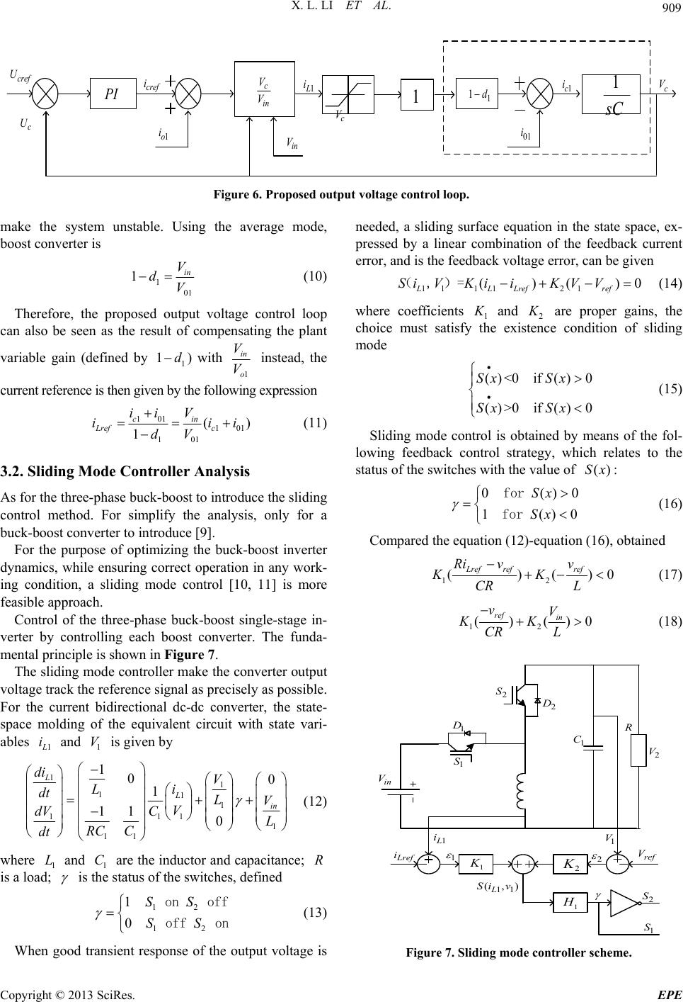 X. L. LI ET AL. 909 sC 1 PI 1 cref U c U cref i 1o i 1 L i in V 1 1d 01 i 1c i c V c V c in V V Figure 6. Proposed output voltage control loop. ake the system unstable. Using the average mode, m boost converter is 101 1in V dV (10) Therefore, the proposed output voltage control loop can also be seen as the result of compensating the plant variable gain (defined by ) with 1 1d 1 in o V instead, the V current reference is then given by the following expression 101 101 101 () 1 cin Lref c ii V iii dV (11) 3.2. Sliding Mode Controller Analysis e the sliding ck-boost inverter dy ee-phase buck-boost single-stage in- ve ter output vo As for the three-phase buck-boost to introduc control method. For simplify the analysis, only for a buck-boost converter to introduce [9]. For the purpose of optimizing the bu namics, while ensuring correct operation in any work- ing condition, a sliding mode control [10, 11] is more feasible approach. Control of the thr rter by controlling each boost converter. The funda- mental principle is shown in Figure 7. The sliding mode con troller make the conver ltage track the reference signal as precisely as possible. For the current bidirectional dc-dc converter, the state- space molding of the equivalent circuit with state vari- ables 1 L i and 1 V is given by 11 111 1 111 11 100 1 11 0 L Lin di V Li dt LV V dV CL RC C dt (12) where and are the inductor and capacitance; 1 L d; 1 C R is a loa is t status of the switches, defined 1 SS on off he 12 12 0 SS off on (13) When good transient response of the output voltage is needed, a sliding surface equation in the state space, ex- pressed by a linear combination of the feedback current error, and is the feedback voltage error, can be given 11 1121 ()()0 LLLref ref SiVKiiKVV (,)= (14) 1 K and 2 K where coefficients are proper gai choice mutence condition of sliding (15) Sliding mode control is obtained by means of the fol- lowing feedback control strategy, which relates to the st (16) Compared the equation (12)-equatio ns, the st satisfy the exis mode ()<0 if ()0 ()>0 if ()0 Sx Sx Sx Sx atus of the switches with the value of ()Sx: 0 ()0 1 ()0 Sx Sx for for n (16), obtained 12 ()()0 Lref refref Ri vv KK (17 CR L) 12 ()() ref in vV KK CR L 0 (18) 1 S 1 D 2 S 2 D 1 C R in V 1 K 2 K 1 H 1 L i L ref i 1 11 (,) L Siv 2 S 1 S 2 1 V ref V 2 V Figure 7. Sliding mode controller scheme. Copyright © 2013 SciRes. EPE  X. L. LI ET AL. 910 If the sliding mode exists, the system behavior is com- pletely determined by coefficients 1 K and 2 K . It is determines the system respon The sliding mode function is applied to a hys- teresis comparator se, stability and robustness. ()Sx (1 H ), proby the switch control signal (duced ) in the power switch and . By adjusted 1 S2 S 1 L i and make so as to realize the ac- curate tracg of ohrence signal. In addition, the inductor current is related to the load, the reference value is difficult to determine. Therefore, in practical applications, the inductor current feedback by a high-pass filter, take its high-frequency component to replace the inductor current error, so only need to control the high frequency component of the inductor current. 4. The Analysis of Simulation 4.1. Th ide nd 2 i 1 kin Vthe utp ()Sx ut vo0, ltage of te refe e Result of Simulation The simulation results are given assuming the three- phase input voltage source, power switch, elements such as inductance and capacitanceal. The prototype in- verter parameters a specification are: input voltage 48 in VV, switching frequency 0KHz,nductor 1 L .13mH , three-phase load 123 RRR 32, capacitance 123 54CCC uF , the output frequency is 50Hz, sliding mode controller coefficients 10.25K, 20.54K; double-loop control scheme for each Boost are a current loop bandwidth close to 2KHz and a voltage lo op bandwidth of about 800Hz, both phase margins of 50°. The contrast analysis diagrams are the three-phase boo 23 0LL st double-loop control and three-phase buck-boost sliding phase boost double- ol of load FFT: nt: distortion of the output voltage waveform ve is low; 3) -loop control, w mode control of load voltage: The contrast analyses are three- loop control and sliding mode contr The contrast analyses are the three-phase boost dou- ble- loop control and three-phase buck-boost sliding mode control of capacitance voltage: The contrast analyses are the three-phase Boost dou- ble-loop control and three-phase buck-boost sliding mode control of inductor curre Three-phase buck-boost sliding surface of the sliding mode control: Three-phase boost single-stage inverter load sharp re- duction in 0.05s, the simulation waveform graph is shown below: 4.2. The Simulation Results Analysis 1) Three-phase boost/buck-boost single-stage inverter indicates that regulation of the voltage transfer ratio can be realized optionally and the output voltage can be ac- curately tracked according to the reference given by the change; 2) As can be seen from the Figure 8 and Figure 9 the harmonic for three-phase symmetrical sinusoidal wa From Figure 8 can be seen that the double ithout overshoot system into a steady state quickly. From Figure 9 can be seen sliding mode control of the load voltage startup performance is poorer, before into the sliding mode surface ,the system has overshoot, there is a lot of impulse voltage, and power is not enough; 4) The double-loop control is the direct control of the cur- rent and it has strong robustness to external interference. The buck-boost inverter capacitor voltage stress is lower than the boost inverter, so the switching loss of the for- mer is smaller than the latter, which adopts the double- loop control of output harmonic is smaller than using sliding mode control of output harmonic, as shown in Figure 10 the harmonic is 0.6%, and in Figure 11, the harmonic is 2.05%; 5) Compared with double-loop con- trol, sliding mode control has better tracking. Sliding mode control of the feedback voltage is almost consistent and a given voltage (155.5 V) for 155.4 V, and the feed- back voltage is 156 V in the double-loop con trol; 6) Fig- ure 12 and Figure 13 shows the output capacitor voltage has dc-biased. 00.050.1 0. 15 - 300 - 250 - 200 - 150 - 100 -50 0 50 100 150 200 t/s 载电负 压 Figure 8. Three-phase boost double-loop control of the load. Copyright © 2013 SciRes. EPE  X. L. LI ET AL. 911 00.05 0.1 0.15 -300 -200 -100 0 100 200 300 400 t/s 负载电压 Figrue 9. Three-phase buck-boost sliding mode control of the load voltage. Figure 10. Three-phase boost double-loop control of the load FFT. Figure 11. Three-phase buck-boost sliding mode control of the load FFT. 00.05 0.1 0.15 0 100 200 300 400 500 600 t/s 电容电压 Figure 12. Three-phase boost double- loop control of the capacitance voltage. 00.05 0.10.15 - 100 0 100 200 300 400 500 600 700 t/s 电容电压 Figur . e 13. Three-phase buck-boost sliding mode contr ol of the ca pacitanc e voltage Copyright © 2013 SciRes. EPE  X. L. LI ET AL. 912 0.05 0.1 0.150.2 0.25 -40 -20 0 20 40 60 80 100 t/s 电感电流 Figure 14. Three-phase Boost double-loop co ntr ol of the inductor c urrent. 0.05 0.1 0.15 0.2 0.25 -20 -10 0 10 20 30 40 50 60 t/s 电感电流 Figure 15. Three-phase Buck-boost sliding mode c ontrol of the inductor current. 00.05 0.1 0.15 0.2 0.250.3 -0.5 -0.4 -0.3 -0.2 -0.1 0 0.1 0.2 0.3 0.4 0.5 S(x) 滑模面 Figure 16. Three-phase Buck-boost sliding mode control of sliding surface. 0.01 0.02 0.03 0.04 0.05 0.06 0.070.08 0.090.1 - 200 - 150 - 100 -50 0 50 100 150 200 t/s Figure 17. Three-phase boost double-loop control of the load sharp reduction voltage. Copyright © 2013 SciRes. EPE  X. L. LI ET AL. Copyright © 2013 SciRes. EPE 913 5. Conclusions The paper deals with the topology and comparison of three-phase boost, buck-boost single-stage inverter. A control strategy for the three-phase buck-boost inverter has been proposed in this project in which buck-boost converters of the buck-boost inverter are controlled by means of a sliding mode control, while the three-phase boost inverter in which each boost is controlled are by means of a double-loop control scheme that consists of a new inductor current control inner loop and a new output voltage control outer loop. These loops include several compensations that mak e boost converters. In addition, some feed-forward reg- ulations are also designed to make the system highly ro- bust for both of input voltage and output current distur- bances. The simulation result shows that regulation of the voltage transfer ratio and output frequency can be real- ized optionally by the new converter, furthermore the harmonic distortions of waveform is low and have the advantage, such as robustness, good tracking perform- ance. These new inverter is intended to be used in unin- terruptible power supply (UPS) and ac driver systems design whenever an ac voltage larger than the dc link voltage is needed, with no need of a second power con- version stage. ments [2] Z. X. Yan, J. X. Li, W. Zhang, Q. Zhang, Y. N. Zheng and W. Y. Wu, “Topology Family and the Simulation of “BOOK” Differential Single-stage Stage Inverter,” IEEE, 2010. doi:10.1109/63.737601 e possible an accurate control of th 6. Acknowledge This work was supported by key programs of NSFC(50837003), and by the Program of the Science and Technology Foundation of Hebei province of China (11213943),and also be supported by the Doctor Re- search Fund of Yanshan University(No.B549). REFERENCES [1] R. O. Cáceres and I. Barbi, “A Boost DC–AC Converter: Analysis, Design, and Experimentation,” IEEE, Transac- tions on Power Electronics 19 99, Vol. 14, pp. 134-141. [3] Z. Y. Yan, J. X. Li, Y. N. Zheng and W. Y. Wu, “Re- search of Double-Boost Single-stage Stage DC/AC Con- verter based on SPWM,” Vol. 47, No. 9, 2007, pp. 17-19. [4] N. Vazquez, D. Cones, C. HemaIldez, et a1., “A New Nonlinear Control Strategy for the Boost Inverter,” IEEE International power Electronics Conference, Mexico, 2003. [5] P. Sanchis, A. U. E. Gubía and L. Marroyo, “Boost l Strategy,” IEEE Trans- ol. 20, No. 02, 2005, pp. 343-353. doi:10.1109/TPEL.2004.843000 DC-AC Inverter: A New Contro actions on Power Electronics, V [6] B. Kalaivani, V. K. Chinniyan and J. Jerome, “A Novel Control Strategy for the Boost DC-AC Inverter,” India International Conference on Power Electronics, 2006, pp. 341-344. [7] R. Cáceres, R. Rojas and O. Camacho, “Robust PID Con- trol of a Buck-Boost DC-AC Converter,” IEEE, 1998, pp. 180-185. [8] P. Sanchis, A. Ursua, E. Gubia and L. Marroyo, “Buck- Boost DC-AC inverter: Proposal for a New Control Strategy,” 35th Annual IEEE Power Electronics Special- ists Conference, 2004, pp. 3994-3998. [9] Z. Q. Cai, F. Hong and Wang, “Research on a Sin- ,” Power Supply [11] J. Chen, “The Research of DC-AC Inverter Based on Sliding Mode s, University,2003. gle-stage-stage Buck/Boost Inverter Technologies and Application, Vol. 11, No. 4, 2008, pp. 43-47. [10] H. Ma, T. Zhang and S. L. han, “Analysis and Design of Sliding Mode Control for Novel Buck Inverter,” Transac- tions of China Electrotechnical Society, 2005, Vol. 20, No. 7, pp. 50-56. Control,” Master’s Thesi [12] J. L. Zhu, Z. Yue, X. P. Zhang, S. S. Liu and S. W. Liu, “A Study of BMC and BBMC with High Volt- age Trans- fer Ratio. Proceedings of the CSEE,” 2007, Vol. 27, No. 16, pp. 85-91 |