Energy and Power Engineering, 2013, 5, 857-863
doi:10.4236/epe.2013.54B164 Published Online July 2013 (http://www.scirp.org/journal/epe)
A Single Phase Current Source PFC Converter
Based on UC3854*
Jianbo Yang1, Weiping Zhang2Faris Al-Naemi1Xiaoping Chen2
1Materials and Engineering Research Institute (MERI), Sheffield Hallam University (SHU), Sheffield, UK
2Lab of Green Power & Energy System (GPES), North China University of Technology (NCUT), Beijing, China
Email: jumbo-yang@hotmail.com
Received September, 2012
ABSTRACT
A novel high-power-factor Buck type converter with average current control based on UC 3854 is proposed. The input
current is directly controlled by average current control scheme to deliver sinusoidal input current and to gain a high
power factor. The practical results, which illustrate the proposed control philosophy, were obtained from a 120 W
AC/DC Buck type converter. The power factor can reach 0.97.
Keywords: Current Source; PFC; UC3854
1. Introduction
With the extensive application of high frequency power
supply, severe distortions will be introduced into the in-
put current. Thus, the input current which contains a lot
of harmonics will degrade the Power Factor. Therefore,
high power factor techniques are required [1].
PFC can be divided into two main types by the output.
One is voltage source PFC, and the counterpart is current
source PFC (power factor correction). However, the main
research work has been focusing on the voltage source
PFC for quite a long time. The reason is that capacitor
used in voltage source PFC as an energy storage element
is smaller and cheaper than inductor used in current
source PFC. Therefore, the research and application of
the current source PFC is restricted [2,3]. Nevertheless,
the energy storage problem of current source PFC is go-
ing to be solved by the development of superconducting
technology [4]. As a result, the current source PFC will
be more popular. With the research going deep, the reac-
tive power compensation of the power system [5], active
electric power filter [6], solar and wind energy and other
renewable energy, which are based on current source
PFC, are developing rapidly.
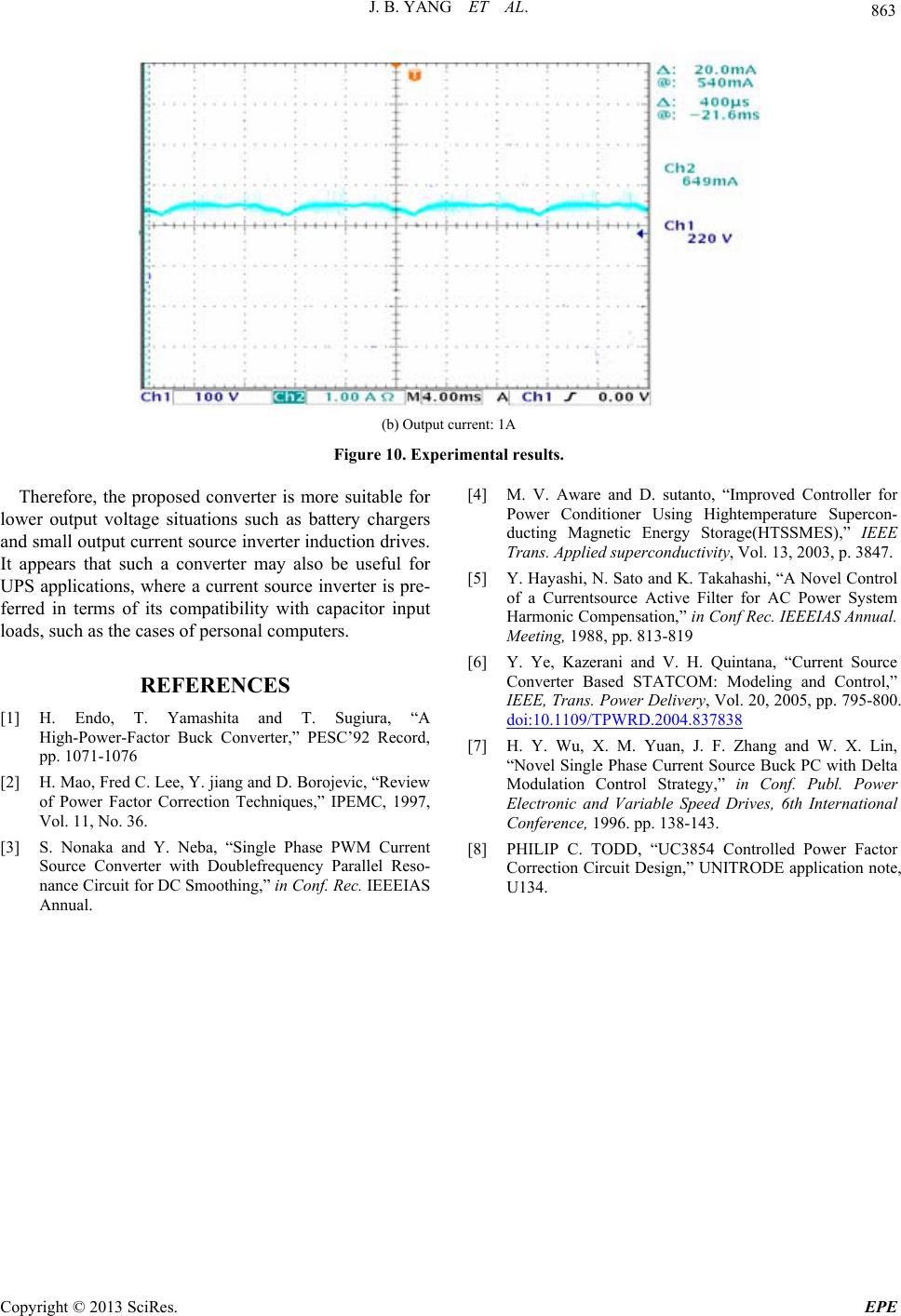
A 120 w single phase current source PFC based on
Buck type converter has been developed in this paper.
With the directly control scheme, the output current can
be kept at 1 A. Also, the output voltage is 200 V which is
lower than the input voltage 220 V (RMS), which over-
comes the disadvantage of the Boost PFC.
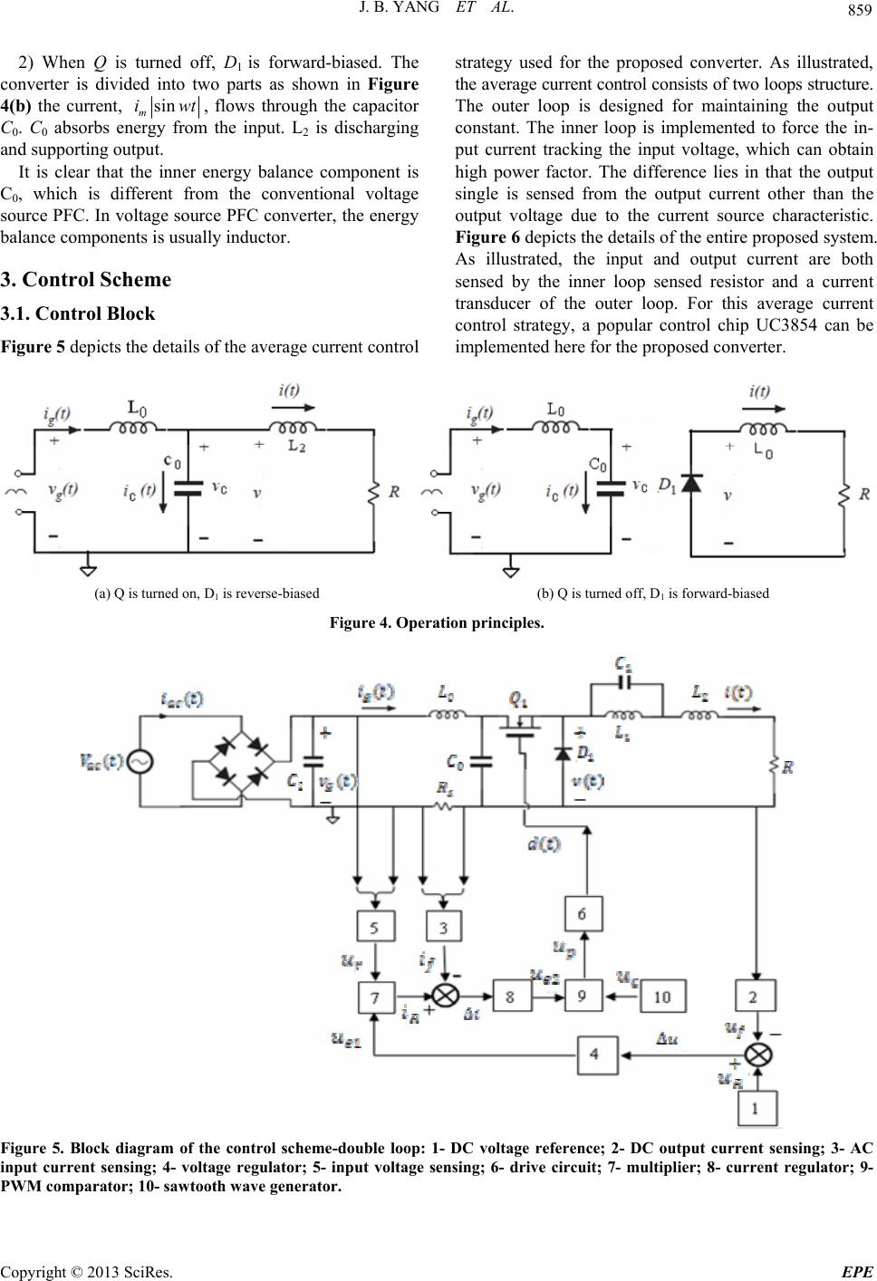
2. Power Stage
2.1. Circuit Configuration
Topologies of the two kinds of PFC mentioned in chapter
1 are actually dual with each other, which is shown is
Figure 1[7]. The power stage of single phase current
source PFC can be suggested in Figure 1(b). One prob-
lem can be found easily is that the input power supply is
an AC current source which is not the same as the AC
voltage source usually used in the normal life. To coun-
teract this inconsistency, an input inductor can be em-
ployed, as shown in Figure 2. The problem is solved as
the input AC voltage supply and the input inductor can
form an analog AC current source. Therefore, the pro-
posed single phase current source PFC base on Buck
topology can be obtained.
The input voltage and input current can be expressed
as follows when the PFC function is accomplished
sin sin
mmout o
uwtiwtuI
(1)
The output voltage is suggested as:
2
sin(1cos 2)
2
mm mm
out oo
ui ui
uwt
II
wt
(2)
There exists a low frequency component which is
twice of line frequency in the output voltage. If only an
inductor servers for filter to file this low frequency ripple,
the size of the inductor at the DC side will be obviously
large. To reduce the size of the inductor at the output side
(L0), a LC parallel resonance net which is in series with
*Project supported by Natural Science foundation of China (N0.
51277004). The Importation and Development of High-Caliber Talents
Project of Beijing Municipal Institutions (No.IDHT20130501)
Copyright © 2013 SciRes. EPE
J. B. YANG ET AL.
858
the output inductor is employed. Figure 3 presents the
suggested converter.
The parallel resonant filter prevents the second har-
monic distortions presenting at the output current. Thus,
the specifications for the filter design are resonant fre-
quency and Q factor. The principles can be given as,
0
11
0
01
1
2
2
o
l
e
wf
LC
ff
R
QwL


(3)
The inductor should be large enough to attenuate the
resonant current which may cause the inductor magnetic
saturation.
2.2. Operation Principles
The parallel net shown in Figure 3 is just used to filter
out the two time of line-frequency harmonic of the output
voltage. The design of the net is provided by (3). Thus,
the net can be out of concern when the operation princi-
ples of the proposed converter are discussed. Therefore,
the operation discussed in this paper is based on the con-
figuration shown in Figure 2. However, the circuit used
in the experiment is based on Figure 3.
When the converter operates as a PFC Preregulator,
the input current will follow the input voltage, which can
be presented as sin
m
iwt
. The operation principles of
the proposed converter shown in Figure 2 are illustrated
in Figure 4. As shown, the average voltage over L0 is
zero in steady state. Thus, the average voltage over C0 is
input voltage, sin
m
Vwt.
1) When Q is turned on, D1 is reverse-biased. The
current flows through the capacitor is
0sin 0
Com
iIi wt
 (4)
Io is the output current which is thought to be constant.
C0 is discharging and transfer energy to load and L2.
(a) Voltage source PFC (b) Current source PFC
Figure 1. Tw o diffe rent type PFC circuits.
Figure 2. Proposed converter.
Figure 3. A proposed converter with parallel net.
Copyright © 2013 SciRes. EPE
J. B. YANG ET AL. 859
2) When Q is turned off, D1 is forward-biased. The
converter is divided into two parts as shown in Figure
4(b) the current, sin
m
iwt, flows through the capacitor
C0. C0 absorbs energy from the input. L2 is discharging
and supporting output.
It is clear that the inner energy balance component is
C0, which is different from the conventional voltage
source PFC. In voltage source PFC converter, the energy
balance components is usually inductor.
3. Control Scheme
3.1. Control Block
Figure 5 depicts the details of the average current control
strategy used for the proposed converter. As illustrated,
the average current control consists of two loops structure.
The outer loop is designed for maintaining the output
constant. The inner loop is implemented to force the in-
put current tracking the input voltage, which can obtain
high power factor. The difference lies in that the output
single is sensed from the output current other than the
output voltage due to the current source characteristic.
Figure 6 depicts the details of the entire proposed system.
As illustrated, the input and output current are both
sensed by the inner loop sensed resistor and a current
transducer of the outer loop. For this average current
control strategy, a popular control chip UC3854 can be
implemented here for the proposed converter.
(a) Q is turned on, D1 is reverse-biased (b) Q is turned off, D
1 is forward-biased
Figure 4. Operation principles.
Figure 5. Block diagram of the control scheme-double loop: 1- DC voltage reference; 2- DC output current sensing; 3- AC
input current sensing; 4- voltage regulator; 5- input voltage sensing; 6- drive circuit; 7- multiplier; 8- current regulator; 9-
WM comparator; 10- sawtooth wave generator.
P
Copyright © 2013 SciRes. EPE
J. B. YANG ET AL.
860
As depicted in Figure 6, the average current control
has the conventional double-loop structure. However, the
difference lies in the output sensing. As the output is a
constant DC current that works as a DC current source.
Thus, the output current is sensed by a current transducer.
Then, this sensed signal is transferred to voltage which is
compared to the reference voltage to make the output
stable. This makes sure that the conventional PFC IC can
be used in this proposed converter.
There are two operational amplifiers and two corre-
sponding compensation network, which is the same as
the conventional average current control scheme used for
the voltage source PFC converter.
3.2. Switching Current Analysis
The power stage of the converter has two different con-
figurations shown in Figure 4. If the input current is as-
sumed to track the input voltage correctly and the output
current can be kept as a constant value, then the wave-
forms of the proposed converter can be depicted as Fig-
ure 7 the output current of the proposed converter will be
higher than the peak of output current. This is very simi-
lar with the relationship of the input voltage and output
voltage of the single phase voltage source Boost PFC.
The modulating voltage and the carried voltage are
both generated by the UC3854, which are used to gener-
ate the switch control signal [8].
s
u is sinusoidal and is
compared with the triangular voltage, c When u
s
c,
a turn-on signal is generated to make the switch open.
When
uu
s
c
uu
, Q will be turned off.
The switch current varies in accordance with the on-
time of the switch. Further analysis can be made that the
switch current can be expanded by Fourier series as,
0
1
cos
2
Qn
n
a
ia
 nwt
(5)
Figure 6. Proposed “double current loop” control strategy,
Figure 7. Waveforms of proposed converters: us—modulating wave; uc—carrier wave; iQ—switch current; iD1—diode cur-
rent.
Copyright © 2013 SciRes. EPE
J. B. YANG ET AL. 861
1~2
in Figure 7 mean the conduction angles in a
quarter of the line cycle. Consequently, the switch cur-
rent can be expressed as,
24
1
135
24
[(1sinsin
sinsinsin)cos]
Q outout
n
iIInn
nnnnn



 
 wt
(6)
The fundamental wave and other harmonics of the
switch current are decided by the conduction angle,
which is decided by the conjunction of the and
c
u
s
u.
4. Results
4.1. Simulations
Simulations using Pspice has been carried out. As shown
in Figure 8, the double-loop control structure is identical
to the theoretical analysis shown in Figure 6. The input
voltage was set to be 220 V (RMS) with 50 Hz frequency.
The switch frequency is 100 kHz. The input power is 200
W and the output power is 170 W. The efficiency is
about 85%.
The results are shown below and prove that the power
factor can be about 0.97 and the output current can be
constant.
4.2. Experiments
A 120 W prototype has been was proposed for verifying
the features of the converter. The experimental results are
in coincidence with the simulations ones. The results are
shown in Figure 10.
5. Conclusions
A high power factor single phase current source con-
verter is proposed in this paper. Input current is directly
controlled by the average current control scheme based
on UC 3854, which forms a particular “double-current-
loop” control programme. Moreover, a parallel resonant
filter is employed to downsize the output inductor. The
proposed converter can deliver a constant DC output
current which can function as a DC current source. In
addition, it does not require that the output voltage has to
be higher than the input voltage.
R11
0.4
R13
100k
C11
220n
R12 0.4 C9 36u
1 2
L3
70mH
R6
220k
+
5
-
6
V+
4
V- 11
OUT 7
U5B
LM324
C4
62n C5
22n
R7
22k
0
V7
15Vdc
R8
3.9k
0
1 2
L2
700u
C2
220n
0
0
Dbreak
D5
Dbreak
D1 Dbreak
Dbreak
D3 Dbreak
D4
V1
FREQ = 50
VAMPL = 310
VOFF = 0R1
100
+
-
+
-
S1
S
VON = 5. 0V
VOFF = 0. 0V
0
OUT+
OUT-
IN+
IN-
E1
V(%IN+, %IN-)
ETABLE
1 2
L1
1.5mH
V5
R2
0.01
0
ABS
0
C7
220n
V11
FREQ = 50
VAMPL = 0.3
VOF F = 0
0
+
-
H2
H
C10
330n
0
V10
15Vdc
0
+5
-6
V+
4
V- 11
OUT
7
U1B
LM324
0
V12
3Vdc
+
-
H3
H
Figure 8. Pspice simulation block.
Copyright © 2013 SciRes. EPE
J. B. YANG ET AL.
862
Time
350ms 360ms 370ms 380ms 390ms400ms
V(D3:2,V1:-)/200 -I(V1)
0
-2.0
2.0
(a) Input voltage: 310v (peak) ; Input current: 1.3A (peak)
Time
300ms 310ms 320ms 330ms340ms 350ms
-I(R1)
0A
-2.0A
3.0A
(b) Output current: 1.4A
Figure 9. Simulation results.
(a) Input voltage: 220V (RMS); Input current: 550mA (RMS) load: 100; Power factor: 0.974
Copyright © 2013 SciRes. EPE
J. B. YANG ET AL.
Copyright © 2013 SciRes. EPE
863
(b) Output current: 1A
Figure 10. Experimental results.
[4] M. V. Aware and D. sutanto, “Improved Controller for
Power Conditioner Using Hightemperature Supercon-
ducting Magnetic Energy Storage(HTSSMES),” IEEE
Trans. Applied superconductivity, Vol. 13, 2003, p. 3847.
Therefore, the proposed converter is more suitable for
lower output voltage situations such as battery chargers
and small output current source inverter induction drives.
It appears that such a converter may also be useful for
UPS applications, where a current source inverter is pre-
ferred in terms of its compatibility with capacitor input
loads, such as the cases of personal computers.
[5] Y. Hayashi, N. Sato and K. Takahashi, “A Novel Control
of a Currentsource Active Filter for AC Power System
Harmonic Compensation,” in Conf Rec. IEEEIAS Annual.
Meeting, 1988, pp. 813-819
[6] Y. Ye, Kazerani and V. H. Quintana, “Current Source
Converter Based STATCOM: Modeling and Control,”
IEEE, Trans. Power Delivery, Vol. 20, 2005, pp. 795-800.
doi:10.1109/TPWRD.2004.837838
REFERENCES
[1] H. Endo, T. Yamashita and T. Sugiura, “A
High-Power-Factor Buck Converter,” PESC’92 Record,
pp. 1071-1076 [7] H. Y. Wu, X. M. Yuan, J. F. Zhang and W. X. Lin,
“Novel Single Phase Current Source Buck PC with Delta
Modulation Control Strategy,” in Conf. Publ. Power
Electronic and Variable Speed Drives, 6th International
Conference, 1996. pp. 138-143.
[2] H. Mao, Fred C. Lee, Y. jiang and D. Borojevic, “Review
of Power Factor Correction Techniques,” IPEMC, 1997,
Vol. 11, No. 36.
[3] S. Nonaka and Y. Neba, “Single Phase PWM Current
Source Converter with Doublefrequency Parallel Reso-
nance Circuit for DC Smoothing,” in Conf. Rec. IEEEIAS
Annual.
[8] PHILIP C. TODD, “UC3854 Controlled Power Factor
Correction Circuit Design,” UNITRODE application note,
U134.