Paper Menu >>
Journal Menu >>
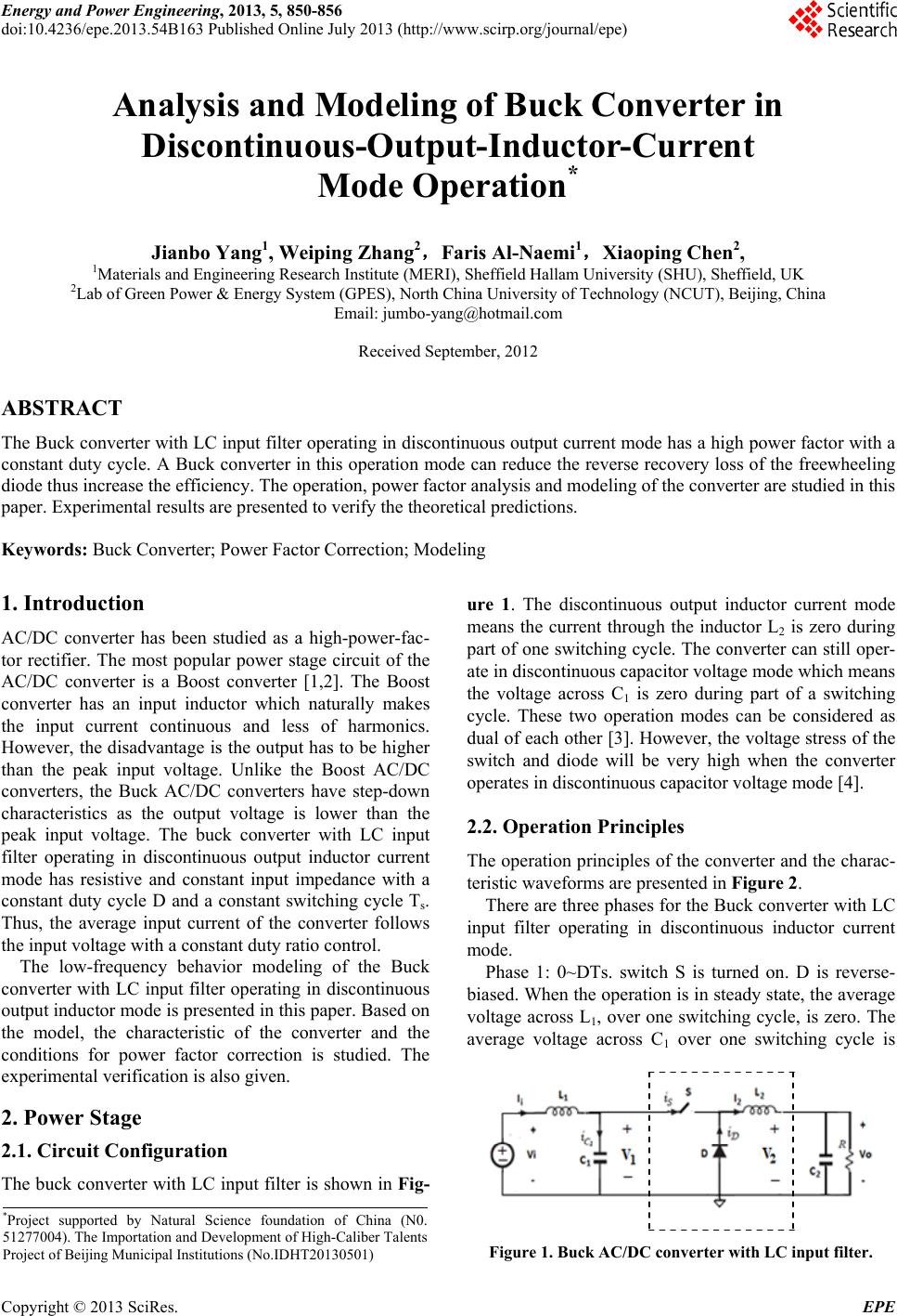 Energy and Power Engineering, 2013, 5, 850-856 doi:10.4236/epe.2013.54B163 Published Online July 2013 (http://www.scirp.org/journal/epe) Analysis and Modeling of Buck Converter in Discontinuous-Output-Inductor-Current Mode Operation* Jianbo Yang1, Weiping Zhang2,Faris Al-Naemi1,Xiaoping Chen2, 1Materials and Engineering Research Institute (MERI), Sheffield Hallam University (SHU), Sheffield, UK 2Lab of Green Power & Energy System (GPES), North China University of Technology (NCUT), Beijing, China Email: jumbo-yang@hotmail.com Received September, 2012 ABSTRACT The Buck converter with LC input filter operating in discontinuous output current mode has a high power factor with a constant duty cycle. A Buck converter in this operation mode can reduce the reverse recovery loss of the freewheeling diode thus increase the efficiency. The operation, power factor analysis and modeling of the converter are studied in this paper. Experimental results are presented to verify the theoretical predictions. Keywords: Buck Converter; Power Factor Correction; Modeling 1. Introduction AC/DC converter has been studied as a high-power-fac- tor rectifier. The most popular power stage circuit of the AC/DC converter is a Boost converter [1,2]. The Boost converter has an input inductor which naturally makes the input current continuous and less of harmonics. However, the disadvantage is the output has to be higher than the peak input voltage. Unlike the Boost AC/DC converters, the Buck AC/DC converters have step-down characteristics as the output voltage is lower than the peak input voltage. The buck converter with LC input filter operating in discontinuous output inductor current mode has resistive and constant input impedance with a constant duty cycle D and a constant switching cycle Ts. Thus, the average input current of the converter follows the input voltage with a constant duty ratio control. The low-frequency behavior modeling of the Buck converter with LC input filter operating in discontinuous output inductor mode is presented in this paper. Based on the model, the characteristic of the converter and the conditions for power factor correction is studied. The experimental verification is also given. 2. Power Stage 2.1. Circuit Configuration The buck converter with LC input filter is shown in Fig- ure 1. The discontinuous output inductor current mode means the current through the inductor L2 is zero during part of one switching cycle. The converter can still oper- ate in discontinuous capacitor voltage mode which means the voltage across C1 is zero during part of a switching cycle. These two operation modes can be considered as dual of each other [3]. However, the voltage stress of the switch and diode will be very high when the converter operates in discontinuous capacitor voltage mode [4]. 2.2. Operation Principles The operation principles of the converter and the charac- teristic waveforms are presented in Figure 2. There are three phases for the Buck converter with LC input filter operating in discontinuous inductor current mode. Phase 1: 0~DTs. switch S is turned on. D is reverse- biased. When the operation is in steady state, the average voltage across L1, over one switching cycle, is zero. The average voltage across C1 over one switching cycle is *Project supported by Natural Science foundation of China (N0. 51277004). The Importation and Development of High-Caliber Talents Project of Beijing Municipal Institutions (No.IDHT20130501) Figure 1. Buck AC/DC converter with LC input filter. Copyright © 2013 SciRes. EPE 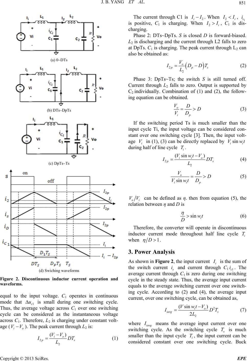 J. B. YANG ET AL. 851 (a) 0~DTs (b) DTs~DpTs (c) DpTs~Ts (d) Swiching waveforms Figure 2. Discontinuous inductor current operation and waveforms. equal to the input voltage. C1 operates in continuous mode that 1c is small during one switching cycle. Thus, the average voltage across C1 over one switching cycle can be considered as the instantaneous voltage across C1. Therefore, L2 is charging under constant volt- age (V). The peak current through L2 is: u o V i 2 2 () io p s VV I DT L (1) The current through C1 is 2i I I. When 2i I I , 1 c is positive, C1 is charging. When i 2i I I, C1 is dis- charging. Phase 2: DTs~DpTs. S is closed D is forward-biased. L2 is discharging and the current through L2 falls to zero at DpTs. C1 is charging. The peak current through L2 can also be obtained as: 2 2 o p p V s I DDT L (2) Phase 3: DpTs~Ts; the switch S is still turned off. Current through L2 falls to zero. Output is supported by C2 individually. Combination of (1) and (2), the follow- ing equation can be obtained. i o p V VDD D (3) If the switching period Ts is much smaller than the input cycle Ti, the input voltage can be considered con- stant over one switching cycle [3]. Then, the input volt- age i in (1), (3) can be directly replaced by during half of line cycle . Vsin ii Vwt i T 2 2 (sin ) iio p s VwtV I DT L (4) sn i ii o p Vwt VDD D (5) io VV can be defined as η. then from equation (5), the relation between η and D is sin i wt D (6) Therefore, the converter will operate in discontinuous inductor current mode throughout half line cycle when i T 1D . 3. Power Analysis As shown in Figure 2, the input current i I is the sum of the switch current s i and current through C11c. The average current through C1 is zero during one switching cycle in the steady state. Thus, the average input current equals to the average switching current over one switch- ing cycle. According to (2) and (4), the average input current, over one switching cycle, can be obtained as, i 2 2 (sin ) 2 io iavg s VwtV I DT L (7) where iavg means the average input current over one switching cycle. As the switching cycle I s T is much smaller than the input cycle i, the input current can be considered constant over one switching cycle. Buck T Copyright © 2013 SciRes. EPE 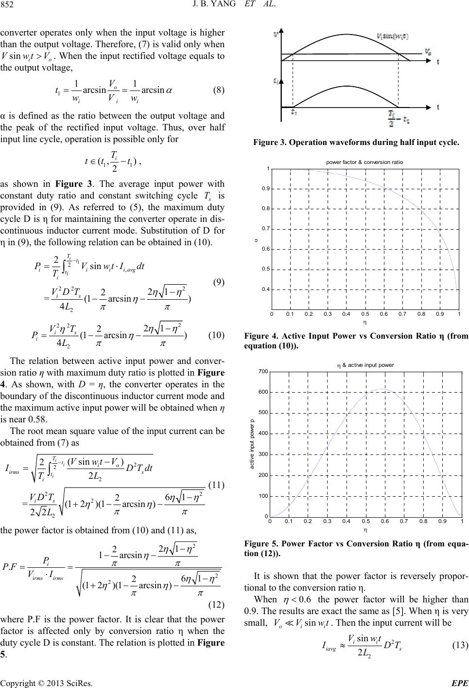 J. B. YANG ET AL. 852 converter operates only when the input voltage is higher than the output voltage. Therefore, (7) is valid only when o . When the input rectified voltage equals to the output voltage, sin i VwtV 1 11 arcsin arcsin o iii V twVw (8) α is defined as the ratio between the output voltage and the peak of the rectified input voltage. Thus, over half input line cycle, operation is possible only for 11 (, ) 2 i T tt t , as shown in Figure 3. The average input power with constant duty ratio and constant switching cycle s T is provided in (9). As referred to (5), the maximum duty cycle D is η for maintaining the converter operate in dis- continuous inductor current mode. Substitution of D for η in (9), the following relation can be obtained in (10). 1 1 2, 2 22 2 2 = Tsin 21 2 (1 arcsin) 4 i Tt iiiiavg t i is PVwtIdt VDT L (9) 2 22 2 21 2 (1 arcsin) 4 is i PVT L (10) The relation between active input power and conver- sion ratio η with maximum duty ratio is plotted in Figure 4. As shown, with D = η, the converter operates in the boundary of the discontinuous inductor current mode and the maximum active input power will be obtained when η is near 0.58. The root mean square value of the input current can be obtained from (7) as 2 2 2 2 2 2 2 (sin ) 2 2 61 2 =(12)(1arcsin) 22 ii i Ttio irms s t i is VwtV IDTdt TL VDT L (11) the power factor is obtained from (10) and (11) as, 2 2 2 21 2 1arcsin . 61 2 (12)(1arcsin ) i irms irms P PF VI (12) where P.F is the power factor. It is clear that the power factor is affected only by conversion ratio η when the duty cycle D is constant. The relation is plotted in Figure 5. t t Figure 3. Operation waveforms during half input cycle. 00.1 0.20.3 0.4 0.50.6 0.70.8 0.91 0.4 0.5 0.6 0.7 0.8 0.9 1 power factor & conversi on rat i o Figure 4. Active Input Power vs Conversion Ratio η (from equation (10)). 00.1 0.2 0.30.4 0.50.60.7 0.80.91 0 100 200 300 400 500 600 700 ac tiv e input power p & active input power Figure 5. Power Factor vs Conversion Ratio η (from equa- tion (12)). It is shown that the power factor is reversely propor- tional to the conversion ratio η. When 0.6 the power factor will be higher than 0.9. The results are exact the same as [5]. When η is very small, . Then the input current will be sin oi VVi wt 2 2 sin 2 ii iavg s Vwt I DT L (13) Copyright © 2013 SciRes. EPE 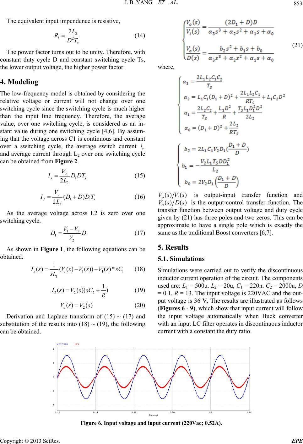 J. B. YANG ET AL. Copyright © 2013 SciRes. EPE 853 The equivalent input impendence is resistive, (21) 2 2 2 i s L RDT (14) The power factor turns out to be unity. Therefore, with constant duty cycle D and constant switching cycle Ts, the lower output voltage, the higher power factor. where, 4. Modeling The low-frequency model is obtained by considering the relative voltage or current will not change over one switching cycle since the switching cycle is much higher than the input line frequency. Therefore, the average value, over one switching cycle, is considered as an in- stant value during one switching cycle [4,6]. By assum- ing that the voltage across C1 is continuous and constant over a switching cycle, the average switch current s i and average current through L2 over one switching cycle can be obtained from Figure 2. 2 1 2 2 s s V I DDT L (15) 2 21 2 () 21 s V I DDDT L (16) () () oi VsVs is output-input transfer function and () () o VsDs is the output-control transfer function. The transfer function between output voltage and duty cycle given by (21) has three poles and two zeros. This can be approximate to have a single pole which is exactly the same as the traditional Boost converters [6,7]. As the average voltage across L2 is zero over one switching cycle. 12 1 2 VV D V D (17) 5. Results As shown in Figure 1, the following equations can be obtained. 5.1. Simulations 11 1 1 ()(() ()) ()* si 1 I sVsVsVss sL C (18) Simulations were carried out to verify the discontinuous inductor current operation of the circuit. The components used are: L1 = 500u. L2 = 20u, C1 = 220n. C2 = 2000u, D = 0.1, R = 13. The input voltage is 220VAC and the out- put voltage is 36 V. The results are illustrated as follows (Figures 6 - 9), which show that input current will follow the input voltage automatically when Buck converter with an input LC filter operates in discontinuous inductor current with a constant the duty ratio. 222 1 () ()() Is VssCR (19) 2 () () o Vs Vs (20) Derivation and Laplace transform of (15) ~ (17) and substitution of the results into (18) ~ (19), the following can be obtained. 0.12 0.140.16 0.180.20.22 Time ( s ) 0 -2 -4 2 4 VP17/100I9*2 Figure 6. Input voltage and input current (220Vac; 0.52A). 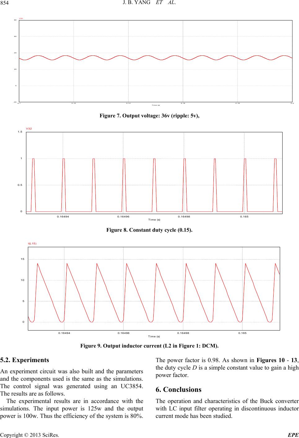 J. B. YANG ET AL. 854 0.10.12 0.14 0.16 0.180.2 Time (s) 0 -20 20 40 60 80 V20 Figure 7. Output voltage: 36v (ripple: 5v), 0.16494 0.164960.164980.165 Time (s) 0 0.5 1 1.5 V32 Figure 8. Constant duty cycle (0.15). 0.16494 0.164960.164980.165 Time (s) 0 5 10 15 I(L15) Figure 9. Output inductor current (L2 in Figure 1: DCM). 5.2. Experiments An experiment circuit was also built and the parameters and the components used is the same as the simulations. The control signal was generated using an UC3854. The results are as follows. The experimental results are in accordance with the simulations. The input power is 125w and the output power is 100w. Thus the efficiency of the system is 80%. The power factor is 0.98. As shown in Figures 10 - 13, the duty cycle D is a simple constant value to gain a high power factor. 6. Conclusions The operation and characteristics of the Buck converter with LC input filter operating in discontinuous inductor current mode has been studied. Copyright © 2013 SciRes. EPE 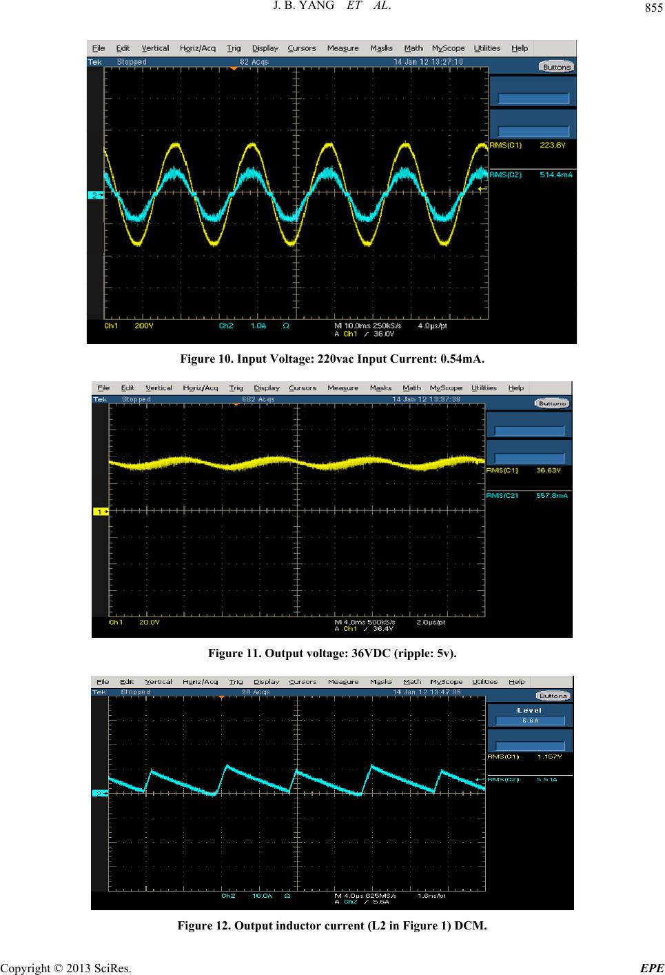 J. B. YANG ET AL. 855 Figure 10. Input Voltage: 220vac Input Current: 0.54mA. Figure 11. Output voltage: 36VDC (ripple: 5v). Figure 12. Output inductor current (L2 in Figure 1) DCM. Copyright © 2013 SciRes. EPE 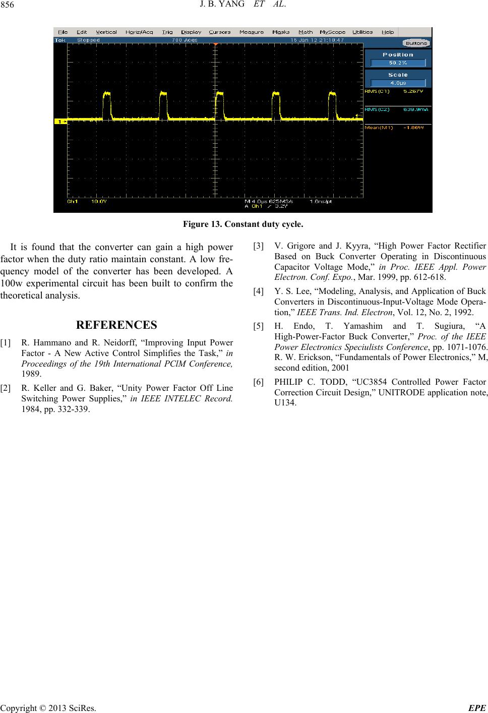 J. B. YANG ET AL. 856 Figure 13. Constant duty cycle. It is found that the converter can gain a high power factor when the duty ratio maintain constant. A low fre- quency model of the converter has been developed. A 100w experimental circuit has been built to confirm the theoretical analysis. REFERENCES [1] R. Hammano and R. Neidorff, “Improving Input Power Factor - A New Active Control Simplifies the Task,” in Proceedings of the 19th International PClM Conference, 1989. [2] R. Keller and G. Baker, “Unity Power Factor Off Line Switching Power Supplies,” in IEEE INTELEC Record. 1984, pp. 332-339. [3] V. Grigore and J. Kyyra, “High Power Factor Rectifier Based on Buck Converter Operating in Discontinuous Capacitor Voltage Mode,” in Proc. IEEE Appl. Power Electron. Conf. Expo., Mar. 1999, pp. 612-618. [4] Y. S. Lee, “Modeling, Analysis, and Application of Buck Converters in Discontinuous-Input-Voltage Mode Opera- tion,” IEEE Trans. Ind. Electron, Vol. 12, No. 2, 1992. [5] H. Endo, T. Yamashim and T. Sugiura, “A High-Power-Factor Buck Converter,” Proc. of the IEEE Power Electronics Speciulists Conference, pp. 1071-1076. R. W. Erickson, “Fundamentals of Power Electronics,” M, second edition, 2001 [6] PHILIP C. TODD, “UC3854 Controlled Power Factor Correction Circuit Design,” UNITRODE application note, U134. Copyright © 2013 SciRes. EPE |