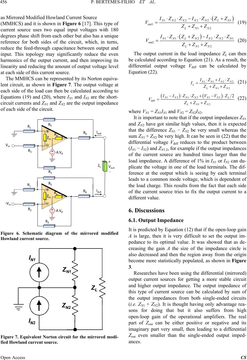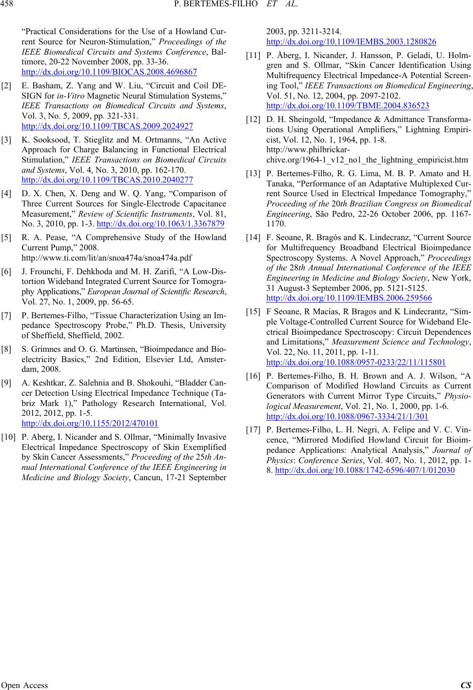
P. BERTEMES-FILHO ET AL.
Open Access CS
458
“Practical Considerations for the Use of a Howland Cur-
rent Source for Neuron-Stimulation,” Proceedings of the
IEEE Biomedical Circuits and Systems Conference, Bal-
timore, 20-22 November 2008, pp. 33-36.
http://dx.doi.org/10.1109/BIOCAS.2008.4696867
[2] E. Basham, Z. Yang and W. Liu, “Circuit and Coil DE-
SIGN for in-Vitro Magnetic Neural Stimulation Systems,”
IEEE Transactions on Biomedical Circuits and Systems,
Vol. 3, No. 5, 2009, pp. 321-331.
http://dx.doi.org/10.1109/TBCAS.2009.2024927
[3] K. Sooksood, T. Stieglitz and M. Ortmanns, “An Active
Approach for Charge Balancing in Functional Electrical
Stimulation,” IEEE Transactions on Biomedical Circuits
and Systems, Vol. 4, No. 3, 2010, pp. 162-170.
http://dx.doi.org/10.1109/TBCAS.2010.2040277
[4] D. X. Chen, X. Deng and W. Q. Yang, “Comparison of
Three Current Sources for Single-Electrode Capacitance
Measurement,” Review of Scientific Instruments, Vol. 81,
No. 3, 2010, pp. 1-3. http://dx.doi.org/10.1063/1.3367879
[5] R. A. Pease, “A Comprehensive Study of the Howland
Current Pump,” 2008.
http://www.ti.com/lit/an/snoa474a/snoa474a.pdf
[6] J. Frounchi, F. Dehkhoda and M. H. Zarifi, “A Low-Dis-
tortion Wideband Integrated Current Source for Tomogra-
phy Applications,” European Journal of Scientific Research,
Vol. 27, No. 1, 2009, pp. 56-65.
[7] P. Bertemes-Filho, “Tissue Characterization Using an Im-
pedance Spectroscopy Probe,” Ph.D. Thesis, University
of Sheffield, Sheffield, 2002.
[8] S. Grimnes and O. G. Martinsen, “Bioimpedance and Bio-
electricity Basics,” 2nd Edition, Elsevier Ltd, Amster-
dam, 2008.
[9] A. Keshtkar, Z. Salehnia and B. Shokouhi, “Bladder Can-
cer Detection Using Electrical Impedance Technique (Ta-
briz Mark 1),” Pathology Research International, Vol.
2012, 2012, pp. 1-5.
http://dx.doi.org/10.1155/2012/470101
[10] P. Aberg, I. Nicander and S. Ollmar, “Minimally Invasive
Electrical Impedance Spectroscopy of Skin Exemplified
by Skin Cancer Assessments,” Proceeding of the 25th An-
nual International Conference of the IEEE Engineering in
Medicine and Biology Society, Cancun, 17-21 September
2003, pp. 3211-3214.
http://dx.doi.org/10.1109/IEMBS.2003.1280826
[11] P. Åberg, I. Nicander, J. Hansson, P. Geladi, U. Holm-
gren and S. Ollmar, “Skin Cancer Identification Using
Multifrequency Electrical Impedance-A Potential Screen-
ing Tool,” IEEE Transactions on Biomedical Engineering,
Vol. 51, No. 12, 2004, pp. 2097-2102.
http://dx.doi.org/10.1109/TBME.2004.836523
[12] D. H. Sheingold, “Impedance & Admittance Transforma-
tions Using Operational Amplifiers,” Lightning Empiri-
cist, Vol. 12, No. 1, 1964, pp. 1-8.
http://www.philbrickar-
chive.org/1964-1_v12_no1_the_lightning_empiricist.htm
[13] P. Bertemes-Filho, R. G. Lima, M. B. P. Amato and H.
Tanaka, “Performance of an Adaptative Multiplexed Cur-
rent Source Used in Electrical Impedance Tomography,”
Proceeding of the 20th Brazilian Congress on Biomedical
Engineering, São Pedro, 22-26 October 2006, pp. 1167-
1170.
[14] F. Seoane, R. Bragós and K. Lindecranz, “Current Source
for Multifrequency Broadband Electrical Bioimpedance
Spectroscopy Systems. A Novel Approach,” Proceedings
of the 28th Annual International Conference of the IEEE
Engineering in Medicine and Biology Society, New York,
31 August-3 September 2006, pp. 5121-5125.
http://dx.doi.org/10.1109/IEMBS.2006.259566
[15] F Seoane, R Macías, R Bragos and K Lindecrantz, “Sim-
ple Voltage-Controlled Current Source for Wideband Ele-
ctrical Bioimpedance Spectroscopy: Circuit Dependences
and Limitations,” Measurement Science and Technology,
Vol. 22, No. 11, 2011, pp. 1-11.
http://dx.doi.org/10.1088/0957-0233/22/11/115801
[16] P. Bertemes-Filho, B. H. Brown and A. J. Wilson, “A
Comparison of Modified Howland Circuits as Current
Generators with Current Mirror Type Circuits,” Physio-
logical Measurement, Vol. 21, No. 1, 2000, pp. 1-6.
http://dx.doi.org/10.1088/0967-3334/21/1/301
[17] P. Bertemes-Filho, L. H. Negri, A. Felipe and V. C. Vin-
cence, “Mirrored Modified Howland Circuit for Bioim-
pedance Applications: Analytical Analysis,” Journal of
Physics: Conference Series, Vol. 407, No. 1, 2012, pp. 1-
8. http://dx.doi.org/10.1088/1742-6596/407/1/012030