Energy and Power Engineering, 2013, 5, 733-739
doi:10.4236/epe.2013.54B142 Published Online July 2013 (http://www.scirp.org/journal/epe)
The Control Technology Research of the Z-source
Three-phase Four-bridge Arm Inverter
Xiangli Li, Zhaoyang Yan , Keke Pan, Chenghao Ma, Hanhong Qi
Key Lab of Power Electronics for Energy Conservation and Motor Drive of Hebei Province,
Yanshan university, Qinhuangdao, China
Email: lxl@ysu.edu.cn
Received March, 2013
ABSTRACT
Z-source inverter can boost the voltage of the DC-side, allow the two switches of the same bridge arm conducting at the
same time and it has some other advantages. The zero-sequence current flows through the fourth leg of the three-phase
four-leg inverter so the three-phase four-leg inverter can work with unbalanced load. This paper presents a Z-source
three-phase four-leg inverter which combines a Z-source network with three-phase four-leg inverter. The circuit uses
simple SPWM modulation technique and the fourth bridge arm uses fully compensated control method. The inverter
can maintain a symmetrical output voltage when the proposed scheme under the unbalanced load.
Keywords: Z-source Inverter; Three-phase Four-leg inverter; Unbalanced Load; Imbalanced Voltage
1. Introduction
Z-source inverter[1-5] with Buck-Boost characteristic
can boost the low DC power to a specified high voltage,
and the two switches of the same bridge arm can conduct
at the same time. Then there is no longer necessary to
add the dead zone, thereby Z-source inverter can reduce
the harmonic content because of the dead zone setting,
and improve the quality of the power conversion. The
traditional three-phase inverter can not provide pathways
for the zero sequence current which is generated by un-
balanced load, It is only suitable for balanced load.
Three-phase four-bridge arm inverter[6-7] increases a
bridge arm on the basis of the traditional three-bridge
arm inverter structure. And this bridge arm constitutes
midline and then eliminates the need of the midpoint
transformer when the load is unbalanced, reduces the
volume and weight of the system. Dq0 rotating coordi-
nate variables are mutually orthogonal, there is no cou-
pling, they can be individually controlled, but the disad-
vantage of this method is the large amount calculation of
the coordinate transformation and coordinate inverse
transformation[8]. The paper separates the fourth bridge
arm from the other control coupled bridge arm. The
fourth bridge arm is individually controlled. Based on the
advantages of the Z-source network and three-phase
four-bridge arm inverter, this paper presents Z source
three-phase four- bridge arm inverter, and it can improve
the voltage pressure, under the unbalanced load it is able
to maintain a good symmetrical output voltage.
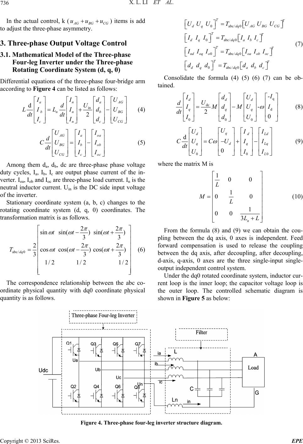
2. Analysis of the Main Circuit
2.1. The Main Circuit
The main circuit is shown in Figure 1. Z-source imped-
ance network is provided by the diode D, capacitor C1,
C2 and inductors L1, L2.In the design of the Z imped-
ance network, the capacitance value of C1, C2 is equal
and the inductance value of L1, L2 is equal. And the
formula is C1 = C2 = C, L1 = L2 = L.
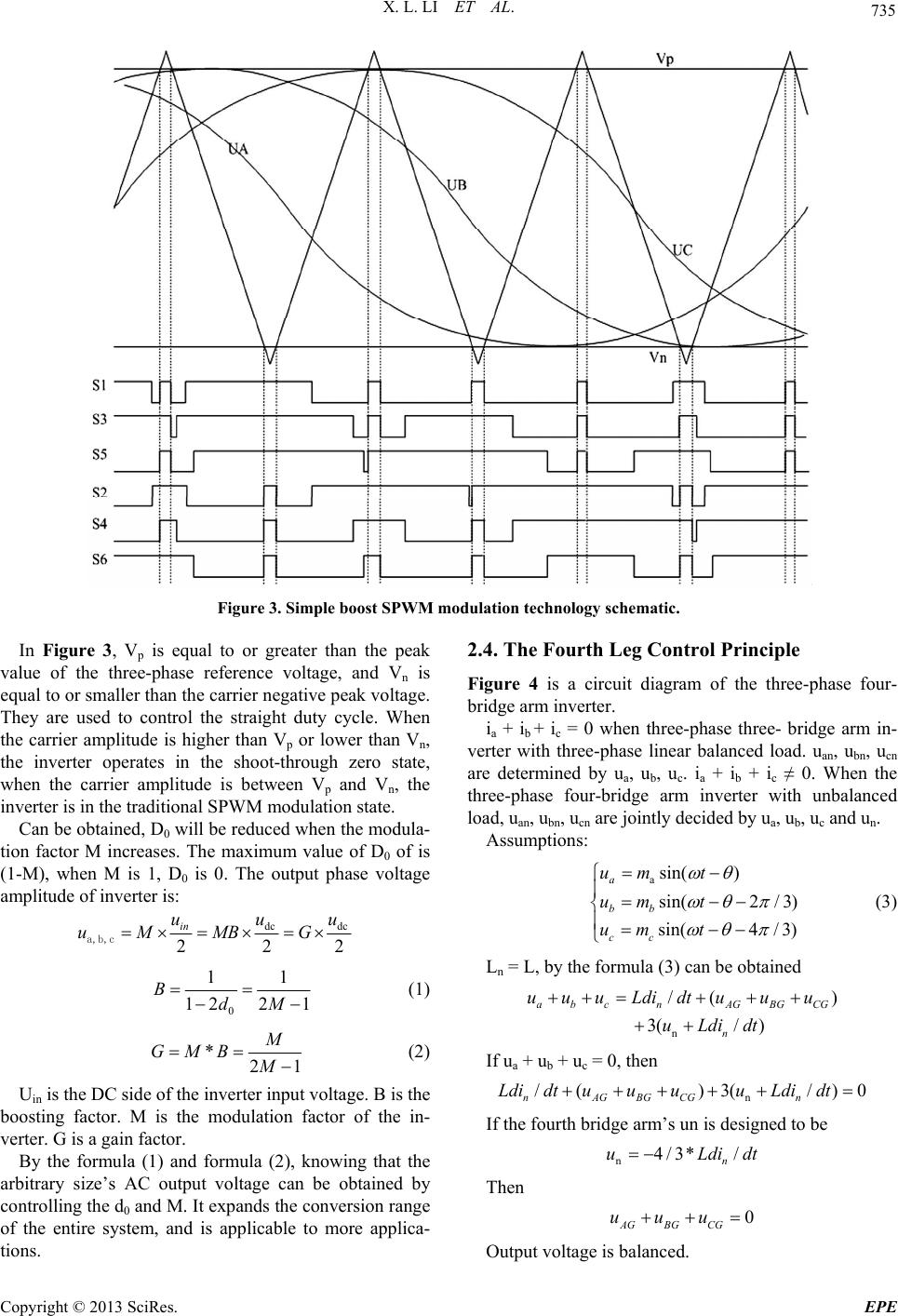
The fourth bridge arm of the three-phase four- bridge
arm inverter is added to the traditional three-phase three
arms. The fourth bridge arm consists of switching tube
Q7, Q8. The midpoint of the bridge arm connects the in-
ductor Ln to the load neutral point. The main function of
the inductance Ln is to filter the switching ripple of the
neutral current. Z-source network and three-phase four-
bridge arm inverter are combined to form a Z -source
three-phase four-bridge arm inverter. The DC voltage
Udc boost by the Z-source network then changes into
alternating current through the four-leg inverter then the
alternating current powers the unbalanced load through
the LC filter.
2.2. Working Principle of Z-source Inverter
Z-source inverter has two working conditions which are
the active state and the shoot-through state. The inverter
can be equivalent to a controlled current source iin.
Figure 2(a) shows the active working state of the Z-
source inverter’s equivalent circuit diagram. When the
Copyright © 2013 SciRes. EPE
X. L. LI ET AL.
734
switching state is one of the active state or the traditional
zero vector, the input of the diode D is conducting, the
power source and the inductors L1, L2 simultaneously
power the load, capacitor Cl and C2 are charging status.
Figure 2( a) can be obtained:
12 21
11 21
dc CLCL
inCL C L CL
uuuuu
uuuuuuu


Calculate the above two formulas,we can obtain:
2
inC dc
uuu
where uin is the DC side input voltage .
Figure 2(b) shows the shoot-through working state of
the Z-source inverter’s equivalent circuit diagram. Diode
D is cutoff. Inductor and capacitor exchange energy. Ca-
pacitance charges inductance .We can obtain from Fig-
ure 2 (b):
12 12
in 0
CCCLL
uuuuuu
u

L
The inductor L1 (L2) should satisfy the volt-second
characteristic within a switching period Ts (the average
storage energy of a switching cycle is zero). During a
switching cycle, anti-shoot-through state works time is
T1, shoot- through state works time is T0,and T1 + T0 =
Ts, d0 is the straight-through duty cycle. Then we can
obtain:
10
0
1
10 0
0
() 0
1
12
1
12
dc CC
Cdc
in dc
uuTuT
d
T
uu
TT d
uu
d
dc
u



It can be seen that when T 0 varies within the range of
0-0.5T, Uin / Udc is theoretical from 1 to infinity.
2.3. The Simple Boost SPWM Modulation Me-
thod
The basic idea of the Z source three-phase inverter SPWM
modulation is as follows. When Z-source inverter works
in traditional zero vector state and shoot-through zero
vector state, the three-phase load is short-circuited. Re-
place the part time of the traditional zero vector time
with the shoot-through zero vector time, keep the effec-
tive vector works time the same, and then can increase
the output voltage value of the Z-source inverter. The
modulation principle is shown in Figure 3.
Figure 1. The main circuit topology of Z-source three-phase four-leg inverter.
Figure 2. The status of the Z-source inverter.
Copyright © 2013 SciRes. EPE
X. L. LI ET AL. 735
Figure 3. Simple boost SPWM modulation technology sche matic .
In Figure 3, Vp is equal to or greater than the peak
value of the three-phase reference voltage, and Vn is
equal to or smaller than the carrier negative peak voltage.
They are used to control the straight duty cycle. When
the carrier amplitude is higher than Vp or lower than Vn,
the inverter operates in the shoot-through zero state,
when the carrier amplitude is between Vp and Vn, the
inverter is in the traditional SPWM modulation state.
Can be obtained, D0 will be reduced when the modula-
tion factor M increases. The maximum value of D0 of is
(1-M), when M is 1, D0 is 0. The output phase voltage
amplitude of inverter is:
dc dc
22
in
uu
uMMB G 
a,b,c 2
u
0
11
122 1
BdM


(1)
*21
M
GMB
M

(2)
Uin is the DC side of the inverter input voltage. B is the
boosting factor. M is the modulation factor of the in-
verter. G is a gain factor.
By the formula (1) and formula (2), knowing that the
arbitrary size’s AC output voltage can be obtained by
controlling the d0 and M. It expands the conversion range
of the entire system, and is applicable to more applica-
tions.
2.4. The Fourth Leg Control Principle
Figure 4 is a circuit diagram of the three-phase four-
bridge arm inverter.
ia + ib + ic = 0 when three-phase three- bridge arm in-
verter with three-phase linear balanced load. uan, ubn, ucn
are determined by ua, ub, uc. ia + ib + ic 0. When the
three-phase four-bridge arm inverter with unbalanced
load, uan, ubn, ucn are jointly decided by ua, ub, uc and un.
Assumptions:
asin( )
sin(2/ 3)
sin(4/ 3)
a
bb
cc
um t
um t
um t

 
 



(3)
Ln = L, by the formula (3) can be obtained
n
/(
3(/)
a b cnAGBGCG
n
uuuLdi dtuuu
uLdidt
 

)
0
If ua + ub + uc = 0, then
n
/()3( /)
nAGBGCGn
Ldi dtuuuuLdi dt
 
If the fourth bridge arm’s un is designed to be
n4/3* /
n
uLdi dt
Then
0
AG BG CG
uuu

Output voltage is balanced.
Copyright © 2013 SciRes. EPE
X. L. LI ET AL.
736
In the actual control, k (AG BG) items is add
to adjust the three-phase asymmetry.
CG
uuu
3. Three-phase Output Voltage Control
3.1. Mathematical Model of the Three-phase
Four-leg Inverter under the Three-phase
Rotating Coordinate System (d, q, 0)
Differential equations of the three-phase four-bridge arm
according to Fig u r e 4 can be listed as follows:
in
d
2
ana
bn nbBG
cnc
IId
U
d
LILIdU
dt dt
IId
 
 

 
 
 
AG
CG
U
U
(4)
AGa oa
B
Gbob
CGc oc
UII
d
CUI I
dt UII






(5)
Among them da, db, dc are three-phase phase voltage
duty cycles, Ia, Ib, Ic are output phase current of the in-
verter. Ioa, Iob and Ioc are three-phase load current. In is the
neutral inductor current. Uin is the DC side input voltage
of the inverter.
Stationary coordinate system (a, b, c) changes to the
rotating coordinate system (d, q, 0) coordinates. The
transformation matrix is as follows.
abc/ 0
22
sinsin() sin()
33
22
coscos() cos()
33
1/ 21/21/ 2
dq
tt t
Tttt

 

 


2
3
(6)
The correspondence relationship between the abc co-
ordinate physical quantity with dq0 coordinate physical
quantity is as follows.
0abc/0
0abc/0
o0abc/0
0abc/0
TT
d qdqAG BGCG
TT
dqdq abc
TT
doqodqoa ob oc
TT
dqdq abc
UUUTUUU
IIITIII
IIIT III
ddd Tddd
















(7)
Consolidate the formula (4) (5) (6) (7) can be ob-
tained.
q
dc
d
000
-
-
20
ddd
qqq
I
IdU
U
d
Md MUI
dt IdU
  
  

  
  
 
(8)
00
d
0
q
dd
qdq
L
U
UI
CU CUII
dt UI
0
Ld
Lq
I
I
 




 

 

(9)
where the matrix M is
100
1
0
1
00
3n
L
ML
LL
0
(10)
From the formula (8) and (9) we can obtain the cou-
pling between the dq axis, 0 axes is independent. Feed
forward compensation is used to release the coupling
between the dq axis, after decoupling, after decoupling,
d-axis, q-axis, 0 axes are the three single-input single-
output independent control system.
Under the dq0 rotated coordinate system, inductor cur-
rent loop is the inner loop; the capacitor voltage loop is
the outer loop. The controlled schematic diagram is
shown in Figure 5 as below:
Figure 4. Three-phase four-leg inverter structure diagram.
Copyright © 2013 SciRes. EPE
X. L. LI ET AL. 737
Figure 5. dq0 axis control schematic structure diagram.
3.2. Z-source Network Capacitor Voltage
Control Design Idea
Here is the controlled method of Z-source network ca-
pacitor voltage. The Z-source network capacitor voltage
control block diagram is shown in Figure 5. In the de-
sign of the capacitor voltage out loop, the current inner
loop is regarded as a gain link in the out loop path. Ig-
noring the inverter bridge own loss under the condition
of unity power factor, the active power of the inverter
AC side is equal to the active power of the inverter cir-
cuit DC side, then we can obtain the formula (11).
ad
333
222
in inadq
uiuiuiui
q
(11)
In order to simplify the design of the controlled system,
q axis vector voltage was regarded as the 0 vector volt-
age in the two-phase synchronous rotating coordinate
system (d, q). so formula (11) is converted into formula
(12).
a
33
22
in inad
uiui ui
d
(12)
There are formulas (13), (14) of the Z-source network
as follows.
0
1
212
inc dcdc
uuu u
d

(13)
inZL C
iii
(14)
According to formula (13) and formula (14), formula
15 can be obtained. Where uin is the DC side of the in-
verter input voltage, iin is the DC side of the inverter in-
put current, udc is the power supply of the system. iZL is
the current in the inductor Z-source network.
0
(1 2)
33
22
dd dd
cZLinZL ZL
in dc
uiui d
iii ii
uu
 (15)
So capacitor current ic of the voltage loop can be con-
trolled by controlling the load AC current id and thus
control the capacitor voltage.
4. The Simulation Results
System simulation parameters are as follows:
Three-phase output phase voltage: 1102/50 Hz
Input voltage of the DC side: 330 V
Three-phase filter inductor: 1 mH
Midline inductance: 1mH
Filter capacitor: 25
F
Z-source network inductance: 2 mH
Z-source network capacitor: 3300
F
The next two cases were analyzed: (1) the Z source
three-phase three-leg with unbalanced load (two-phase
no-load, one phase with a load of 50 ohms) (2) Z-source
three-phase four-leg with unbalanced load(two-phase no-
load, one phase with a load of 50 ohms).
From Figure 6, we can see the output waveforms
quality is poor and the load voltage is unbalanced when
Z-source three-phase three-bridge arm inverter circuit is
with unbalanced load.
Copyright © 2013 SciRes. EPE
X. L. LI ET AL.
738
00.02 0.04 0.060.080.10.12
-5
0
5
t /s
Out put c urrent/A
00.02 0.04 0.060.080.10.12
-500
0
500
t /s
Out put voltage/V
Figure 6. Three-phase three-leg simulation waveforms with unbalanced load.
0.10.11 0.12 0.13 0.14 0.150.16 0.17 0.18 0.19 0.2
-4
-2
0
2
4
t /s
Output current
/A
0.10.11 0.12 0.130.14 0.15 0.160.17 0.18 0.19 0.2
-200
-100
0
100
200
t/s
Output v oltage
/V
Figrue 7. Three-phase four-le g with unbalanced load simulation.
From Figure 7, we can see the waveforms in the Z-
source three-phase four-bridge arm inverter system with
the same load have been greatly better. The degree of
imbalance of output voltage is small. But the amplitude
does not have a very good stability in expectation; there
is a growing trend, so the control mode needs to improve.
5. Conclusions
This paper presents a Z-source three-phase four-bridge
arm inverter which combines a Z-source network with
three-phase four-leg inverter. The circuit uses simple
SPWM modulation technique. The three-phase four-
bridge arm use PI control in synchronous rotating coor-
dinate system, the fourth bridge arm use independent
methods to control. The simulation results demonstrate
the Z-source three-phase four-bridge arm inverter can
output three-phase sine wave voltage under unbalanced
load conditions.
REFERENCES
[1] F. Z. Peng, X. P. Fang, B. Gu, et al., “Z-Source Con-
verter,” Transactions of China Electrotechnical Society,
Vol. 19, No. 2, 2004, pp. 47-51.
[2] M. S. Shen, J. Wang, F. Z. Peng, et al., “Maximum Con-
stant Boost Control of the Z-source Inverter,” IEEE In-
dustry Applications Society Annual Meeting, 2004, pp.
142-147.
[3] E. Wit and J. McClure, “Statistics for Microarrays: De-
sign, Analysis, and Inference,” 5th Edition, John Wiley &
Sons Ltd., Chichester, 2004. doi:10.1002/0470011084
[4] X. P. DingZ. M. QianB. Cuiet al., “Fuzzy PID
Controller for DC-link Boost Voltage in Z-source In-
Copyright © 2013 SciRes. EPE
X. L. LI ET AL. 739
verter,” Proceedings of the CSEE, Vol. 28, No. 24, 2008,
pp. 31-38.
[5] P. C. Loh, D. M. Vilathgamuwa, C. J. Gajanayake, Y. R.
Lim and C. W. Teo, “Transient Modeling and Analysis of
Pulse-Width Modulated Z-Source Inverter,” EEEE Trans-
action on Power Electronics, Vol. 22, No. 2, 2009, pp.
498-507.
[6] L. B. Li, Z. G. Zhao, et al., “Study on three-phase photo-
voltaic grid-connected inverter system based on composi-
tive control,” Power System Protection and Control, 2010,
Vol. 38, No. 21, pp. 44-47.
[7] L. Jun, T. C. Green and C. Feng, “Increasing Voltage
Utilization inSplit-Link, Four-Wire Inverters,” IEEE
Trans. on Power Electronics,” Vol. 6, No. 24, 2009, pp.
1562-1569.
[8] P. C. Loh, D. M. Vilathgamuwa, C. J. Gajanayake,
L. T. Wong, C. P. Ang, “Z-Source Current—Type
Inverters: Digital Modulation and Logic Imple-
mentation,” IEEE Transactions on Power Electron-
ics, Vol. 22, No. 1, 2007, pp. 169-177.
doi:10.1109/TPEL.2006.886618
Copyright © 2013 SciRes. EPE