Communications and Network, 2013, 5, 6-10
http://dx.doi.org/10.4236/cn.2013.53B2002 Published Online September 2013 (http://www.scirp.org/journal/cn)
A 30GHz Wideband CMOS Injection-Locked Frequency
Divider for 60GHz Transceiver*
Chunqi Shi, Runxi Zhang, Zongsheng Lai
Institute of Microelectronic Circuits and Systems, East China Normal University, Shanghai, China
Email: cqshi@ee.ecnu.edu.cn, rxzhang@ee.ecnu.edu.cn
Received June, 2013
ABSTRACT
In this paper, a 30 GHz wide locking-range (26.2 GHz-35.7 GHz) direct injection-locked frequency divider (ILFD),
which operating in the millimeter-wave (MMW) band, is presented. The locking range of the ILFD is extended by using
differential injection topology. Besides, varactors are used in RLC resonant tank for extending the frequency tuning
range. The post simulation results show that a wide locking-range of 9.5 GHz (30.7%) is achieved. When the VCO
output frequency varies from 26.85 GHz to 34.42 GHz, the proposed ILFD can achieve divide-by-two correctly. De-
signed in 0.13 μm CMOS technology, the ILFD occupies a core area of 0.76 mm2 while drawing 7 mA of current from
2.5 V power supply.
Keywords: CMOS; Injection-locked Frequency Divider (ILFD); Locking Range; VCO; Wideband
1. Introduction
With rapid advances in CMOS technology, the CMOS
circuit operating in millimeter-wave (MMW) band has
attracted increasing interest and research [1-9], such as
point-to-point communications, image sensing, and au-
tomotive radar systems.
Frequency dividers are key components for frequency
synthesizer in a MMW PLL. Conventionally, current-
mode-logic (CML) static divider [1], Miller divider [2],
and injection-locked frequency divider (ILFD) [3-7] are
widely used in various applications. Among these divid-
ers, the CML static diver covers a wide locking range,
but its input frequency is low and its power consumption
is usually high, compared with ILFDs. For a Miller di-
vider and an ILFD, they have a higher input frequency.
However, their locking ranges are quite limited. To real-
ize a divider higher than 20 GHz, an ILFD may be one of
the good candidates.
This paper describes a differential direct ILFD with
varactors for 802.15.3c transceiver. Several design con-
siderations for the ILFD are analyzed for increasing the
wide locking-range. The paper is organized as follows.
Section 2 describes the 60 GHz communication system
architecture. Section 3 addresses the analysis and design
of an ILFD. Section 4 gives the post simulation result
and the comparison with some state-of-the-art counter-
parts. Finally, section 5 gives the conclusion.
2. System Architecture
Figure 1 shows a block diagram of the proposed 60 GHz
transceiver regulated by 802.15.3c, in which the 60 GHz
LO signal is generated using a frequency double and a 30
GHz PLL. The proposed PLL consists of a phase frequency
detector (PFD), charge pump (CP), loop filter, VCO, high
speed ILFD as a first divide stage and a series of subsequent
frequency CML dividers. According to the system analysis
and simulation, the reference frequency is 58.6 MHz, the
gain of VCO is 5 GHz/V, the tuning range of VCO is from
28.5 GHz to 33 GHz, and the loop width is 750 kHz. The
detail design of ILFD will be discussed. The main design
challenge is to reduce input capacitance while maintaining a
wide operating frequency range.
*This paper is funded by project No. 13511500702, Key Laboratory o
f
Wireless Sense Network & Communication, Shanghai Institute o
f
Microsystem and Information Technology, Chinese Academy of Sci-
ences and ECNU
p
ro
j
ect No. 78210082. Figure 1. Block diagram of 60GHz transceiver.
C
opyright © 2013 SciRes. CN
C. Q. SHI ET AL. 7
3. Circuit Implementation
A conventional LC-based ILFD is shown in Figure 2(a).
The input stage Min is used to provide both an input sig-
nal path and a DC bias path. Thus, Min is typically large,
resulting in a large input capacitance. Moreover, the in-
put signal is significantly degraded by the parasitic ca-
pacitor Ctail. By using a peaking inductor between the
drain terminal of Min and the ground, this problem can be
solved; however, this strategy requires a larger die area.
A direct LC-based ILFD is shown in Figure 2(b), it pro-
vides a solution for MMW operation with a low input
capacitance, but it suffers from a narrow locking range.
3.1. Circuit Structure
For wide locking range, the proposed differential ILFD
circuit for high-speed operation is shown in Figure 3.
The ILFD composed of a conventional LC-VCO, varac-
tors, output buffers, and two transistors (M5, M6) receive
the differential injection signals. A complementary cross-
coupled pair is used to implement the active gm.
3.2. Locking Range
In Figure 3, the input transistor M5 and M6 are directly
connected to the drain nodes of the differential cross-
coupled pair (M1, M2 and M3, M4). An equivalent mod-
el of single input transistor is given in Figure 4.
(a) (b)
Figure 2. Conventional ILFD.
Figure 3. The proposed differential ILFD.
Figure 4. Equivalent model.
Ractive is the equivalent resistance of cross-coupled pair;
R, L, and C represent the equivalent passive load.
Assume that, ()cos(2 )
inB i
VtV Vt

() cos
oCMo
Vt VVt
and ()cos(2 )
inB i
VtV Vt

where θ stands for the phase difference between the input
and the output. The input current Iin can be expressed [8]
by separating its in-phase and quadrature phase compo-
nents as
,
( )[4()2cos]cos
(2sin)sin
inBCMth inio
io
tKVVV KVV
KVV t
t

 
 (1)
where (/)/2
nox in
KCWL
.
Iin in equation (1), can also be expressed by phasor as
00
,0, ,0
00
,
90 90
,
4() 2
(2cos )(cos )
(2sin )(sin )
jj
inBCMthinoino
jj
in iioMAXo
jj
in qoMAXo
KVVVVegV e
IKV VegVe
I
KVVegV e







  
(2)
where g
in,0 is the equivalent conductance of the input
transistor and gMAX is the equivalent transconductance of
the input transistor.
The locking range is derived from two aspects, that is
the phase condition and the gain condition.
According the magnitude and phase phasors at node
Vo+ shown in Figure 4, the following equality is given:
0
CLin
III
 (3)
When the input frequency ωin is equal to 2ω0, it result
in ,
0, 0
CL inq
II I
, and 180
.
When ωin is large than 2ω0, the magnitude of IC be-
comes larger than that of I
L. The input current should
increase the quadrature component Iin,q to compensate it.
The corresponding current phasors are shown in Figure
5(a). Similarly, when ωin is smaller the 2ω0, the corre-
sponding current phasors are shown in Figure 5(b).
While the magnitude of Iin,q is at its maximum, θ is
equal to 90º or 270º. The input frequency at this time is
defined as the highest locking frequency, 2ωH, and the
lowest locking frequency, 2ωL, respectively. The phase
Copyright © 2013 SciRes. CN
C. Q. SHI ET AL.
8
(a) 2ω0<ωin<2ωH (b) 2ωL<ωin<2ω0
Figure 5. Current phasors diagram.
shift of the RLC network between ω0 and ωH or ωL is
expressed as
,
0
0
||2
tan( ),
||
in qeffff
Leff
CCP
e
0
I
Q
QR
I
L

  (4)
where Reff is the effective resistance seen by the input
transistor. By the phase condition, the locking range (LR)
referred to the input is derived as
2
0
0
e
22
4() R
MAX MAX
phase L
ffmm ff
Lgg
LR
e
R
g
gC

 (5)
As for gain condition, if there is no input signal, the
loop gain of ILFD should be (gmReff)2 and its value
should exceed unity to assure oscillating. After injection,
the loop gain requirement is given as
2
e
[(cos) R]1
mMAX ff
gg
 (6)
Also, the gain of the input transistor needs to exceed
unity to satisfy the Bark hausen criteria.
The effective impedance of the RLC is expressed as
e
tan 1(2/
ff
k
eff
R
ZjQ )

(7)
The locking range determined by the gain condition is
derived as
e2
e
1
21( )
mff
MAX
gain
MAX ff
gR
g
LR CgR
 (8)
If the ILFD is at the edge of oscillation, the locking
range is simplified as
2
M
AX
gain
g
LR C
(9)
According to equation (5) and (9), in order to increase
the locking range, the capacitance has to be small. Also,
gMAX should be large and it is achieved by increasing the
size and the input magnitude. The size of cross-coupled
pair should be small to realize a smaller gm which will
increase the locking range.
In this design, two input transistors, M5 and M6, are
used to improve the equivalent transconductance. The
simulation results show that the locking range is increase
by 50% compare to single injection topology.
3.3. Tuning Range
The locking range of the ILFD is directly related to its
tuning range. The output frequency of VCO in this de-
sign is from 26.85 GHz to 34.41 GHz. For wide tuning
range, the varactors are used at the output nodes. The
control voltage of ILFD is connected to that of the VCO,
which can realize the synchronous tuning. Thus, the tun-
ing range is extended.
3.4. Output Buffers
The output buffers in Figure 3 are composed of two
stages, the outputs of the first buffer stage are for the
next stage divider, and outputs of second buffer stage are
for testing. The buffers ensure the stability of the loading
capacitance, thus ensure the stability of the tuning fre-
quency.
4. Simulation Results
4.1. Layout and Simulation Results
The layout of the proposed ILFD is shown in Figure 6.
Figure 7 shows the post simulation result of the transient
output waveform. When the control voltage (Vtune) is
equal to 2.5 V, the output frequency of VCO is 34.42
GHz, and the output frequency of ILFD is 17.21 GHz.
Figure 6. Layout of the propose ILFD.
Figure 7. Output waveforms of the proposed ILFD.
Copyright © 2013 SciRes. CN
C. Q. SHI ET AL. 9
Figure 8. Tuning curves of the ILFD.
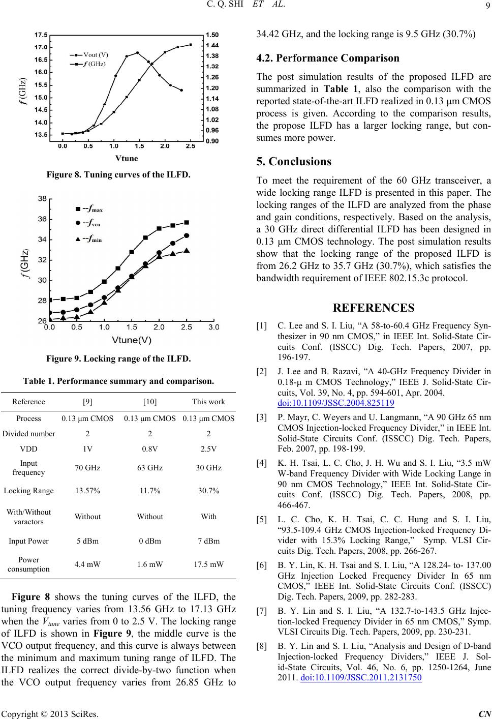
Figure 9. Locking range of the ILFD.
Table 1. Performance summary and comparison.
Reference [9] [10] This work
Process 0.13 μm CMOS 0.13 μm CMOS 0.13 μm CMOS
Divided number 2 2 2
VDD 1V 0.8V 2.5V
Input
frequency 70 GHz 63 GHz 30 GHz
Locking Range 13.57% 11.7% 30.7%
With/Without
varactors Without Without With
Input Power5 dBm 0 dBm 7 dBm
Power
consumption 4.4 mW 1.6 mW 17.5 mW
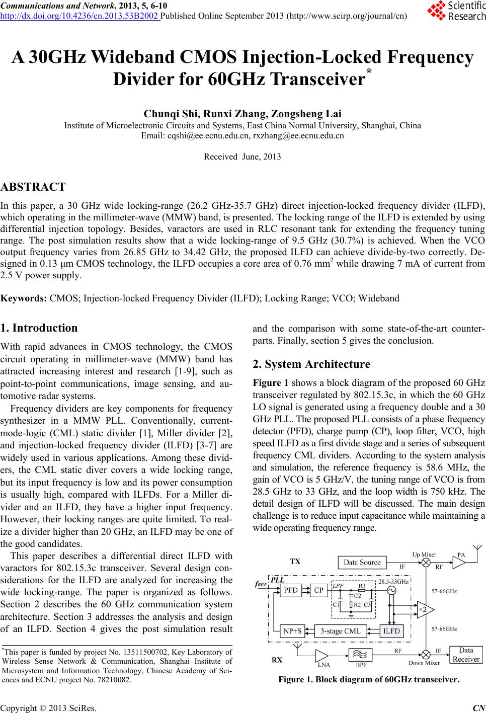
Figure 8 shows the tuning curves of the ILFD, the
tuning frequency varies from 13.56 GHz to 17.13 GHz
when the Vtune varies from 0 to 2.5 V. The locking range
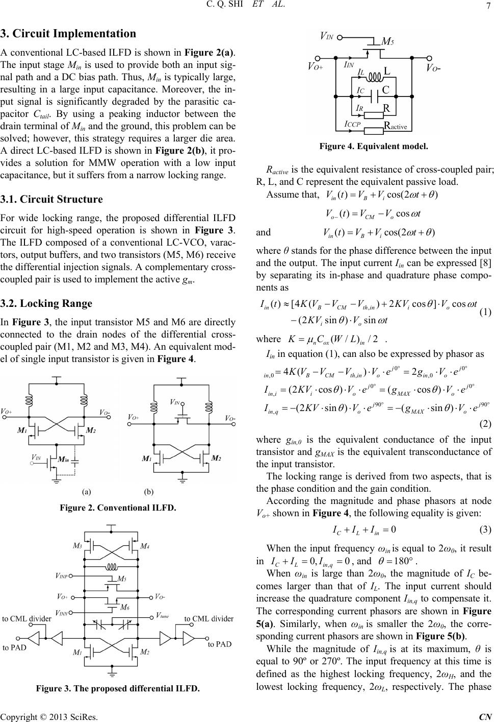
of ILFD is shown in Figure 9, the middle curve is the
VCO output frequency, and this curve is always between
the minimum and maximum tuning range of ILFD. The
ILFD realizes the correct divide-by-two function when
the VCO output frequency varies from 26.85 GHz to
34.42 GHz, and the locking range is 9.5 GHz (30.7%)
4.2. Performance Comparison
The post simulation results of the proposed ILFD are
summarized in Table 1, also the comparison with the
reported state-of-the-art ILFD realized in 0.13 μm CMOS
process is given. According to the comparison results,
the propose ILFD has a larger locking range, but con-
sumes more power.
5. Conclusions
To meet the requirement of the 60 GHz transceiver, a
wide locking range ILFD is presented in this paper. The
locking ranges of the ILFD are analyzed from the phase
and gain conditions, respectively. Based on the analysis,
a 30 GHz direct differential ILFD has been designed in
0.13 μm CMOS technology. The post simulation results
show that the locking range of the proposed ILFD is
from 26.2 GHz to 35.7 GHz (30.7%), which satisfies the
bandwidth requirement of IEEE 802.15.3c protocol.
REFERENCES
[1] C. Lee and S. I. Liu, “A 58-to-60.4 GHz Frequency Syn-
thesizer in 90 nm CMOS,” in IEEE Int. Solid-State Cir-
cuits Conf. (ISSCC) Dig. Tech. Papers, 2007, pp.
196-197.
[2] J. Lee and B. Razavi, “A 40-GHz Frequency Divider in
0.18-μ m CMOS Technology,” IEEE J. Solid-State Cir-
cuits, Vol. 39, No. 4, pp. 594-601, Apr. 2004.
doi:10.1109/JSSC.2004.825119
[3] P. Mayr, C. Weyers and U. Langmann, “A 90 GHz 65 nm
CMOS Injection-locked Frequency Divider,” in IEEE Int.
Solid-State Circuits Conf. (ISSCC) Dig. Tech. Papers,
Feb. 2007, pp. 198-199.
[4] K. H. Tsai, L. C. Cho, J. H. Wu and S. I. Liu, “3.5 mW
W-band Frequency Divider with Wide Locking Lange in
90 nm CMOS Technology,” IEEE Int. Solid-State Cir-
cuits Conf. (ISSCC) Dig. Tech. Papers, 2008, pp.
466-467.
[5] L. C. Cho, K. H. Tsai, C. C. Hung and S. I. Liu,
“93.5-109.4 GHz CMOS Injection-locked Frequency Di-
vider with 15.3% Locking Range,” Symp. VLSI Cir-
cuits Dig. Tech. Papers, 2008, pp. 266-267.
[6] B. Y. Lin, K. H. Tsai and S. I. Liu, “A 128.24- to- 137.00
GHz Injection Locked Frequency Divider In 65 nm
CMOS,” IEEE Int. Solid-State Circuits Conf. (ISSCC)
Dig. Tech. Papers, 2009, pp. 282-283.
[7] B. Y. Lin and S. I. Liu, “A 132.7-to-143.5 GHz Injec-
tion-locked Frequency Divider in 65 nm CMOS,” Symp.
VLSI Circuits Dig. Tech. Papers, 2009, pp. 230-231.
[8] B. Y. Lin and S. I. Liu, “Analysis and Design of D-band
Injection-locked Frequency Dividers,” IEEE J. Sol-
id-State Circuits, Vol. 46, No. 6, pp. 1250-1264, June
2011. doi:10.1109/JSSC.2011.2131750
Copyright © 2013 SciRes. CN
C. Q. SHI ET AL.
Copyright © 2013 SciRes. CN
10
[9] C. Y. Wu and C. Y. Yu, “Design and Analysis of Milli-
meter-wave Direct Injection-locked Frequency Divider
with Large Frequency Locking Range,” IEEE Transac-
tions on Microwave Theory and Techniques, Vol. 55, No.
8, 2007, pp. 1649-1658. doi:10.1109/TMTT.2007.902067
[10] S. J. Rong, W. L. Alan and H. C. Luong, “0.9 mW 7 GHz
and 1.6 mW 60 GHz Frequency Dividers with Lock-
ing-range Enhancement in 0.13 μm CMOS,” IEEE Int.
Solid-State Circuits Conf. (ISSCC) Dig. Tech. Papers,
2009, pp. 96-97.