 Energy and Power Engineering, 2013, 5, 219-225 doi:10.4236/epe.2013.54B043 Published Online July 2013 (http://www.scirp.org/journal/epe) Research on Parallel Interleaved Inverters with Discontinuous Space-Vector Modulation* Feng Yang1, Xu Zhao1, Cong Wang1, ZhiFei Sun2 1China University of Mining & Technology (Beijing), Beijing, China 2Chongqing Research Institute of China Coal Technology & Engineering Group Corporation, Chongqing, China Email: yangfengwy@163.com Received April, 2013 ABSTRACT Parallel converter can significantly increase the capacity of the converter and improve the power quality of AC side, but the circulation which can lead to high switching loss and even damage the devices will easily exist in the direct parallel converters. In this paper, the average model of parallel interleaved inverters system to analyze the circulation current is shown, and the cross current is relevant to DC-bus voltage and the overlap time of zero vectors in the switching period. Based on this observation, a discontinuous space vector modulation without using zero vectors (000) is eliminate and suppress the zero-sequence current to entire system. Finally, the effectiveness of modulation strategy is verified by the simulations in this paper. Keywords: Interleaved Inverters; Circulating Current; Discontinuous Space-vector Modulation; Zero- sequence Current 1. Introduction With the increasing demand for power equipment capac- ity and quality, how to improve the capacity of the power electronic converters and improve its output performance is an important development direction of modern power electronics technology. High-frequency inverters due to the switching frequency and the power devices loss limit, the single component of the inverter only suitable for low or medium capacity occasions. In recent years, in the application of high power applications, the multi-level, mixed topologies, or parallel multiple methods is an ef- fective way for expansion of the capacity of the inverters. Three-phase inverter parallel system has many advan- tages, such as the system can achieve high current level, the current and voltage ripple is small, the parallel sys- tem has higher bandwidth. Previous research on parallel systems are mainly concentrated in the UPS, motor drives, as well as to improve the power factor occasions [1-2,4-6]. With the development of IGBT and other power semiconductor device of intelligent control to the integrated structure, now more and more application modules are directly connected in parallel, especially where a high power density integration is required, such as power sources, traction systems, uninterruptible power supplies, power factor correction circuits and active power filters (APF), and high power photovoltaic power generation system [3,8], through parallel technology to improve converter power and current levels, and enhance the redundancy of the system. therefore, parallel PWM inverter technology is of great significance for the pro- motion of high-power photovoltaic, wind power applica- tions。 Putting modules in parallel, however, is not risk free. One of the major concerns for the parallel operation of a three-phase system is the cross-coupling between the three-phase system parallel modules, i.e., when each module in a certain switching state, the inverter module is connected with a DC bus at the same time to a com- mon power supply or load, to increase the system does not require the circulation loop. In order to avoid this problem, the traditional method is to use an isolation transformer [4-5]. However, the use of transformer will undoubtedly increase the size and cost of the inverter system, especially in the high power and low switching frequency occasions, this problem more prominent. Therefore, the power converter modules are directly connected in parallel is required[3]. Through a comprehensive system analysis using the averaged model, this paper shows the mechanism of how the zero-sequence current is produced with the inter- leaved technology, and the peak of zero-sequence current is related to DC voltage and the overlap time of zero vectors in a switching period. The discontinuous space *National Natural Science Foundation of China. (51077125); The Fundamental Research Funds for the Central Universities. (2010YJ03). Copyright © 2013 SciRes. EPE 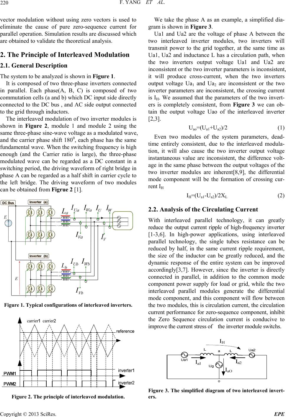 F. YANG ET AL. 220 vector modulation without using zero vectors is used to eliminate the cause of pure zero-sequence current for parallel operation. Simulation results are discussed which are obtained to validate the theoretical analysis. 2. The Principle of Interleaved Modulation 2.1. General Description The system to be analyzed is shown in Figure 1. It is composed of two three-phase inverters connected in parallel. Each phase(A, B, C) is composed of two commutation cells (a and b) which DC input side directly connected to the DC bus , and AC side output connected to the grid through inductors. The interleaved modulation of two inverter modules is shown in Figure 2, module 1 and module 2 using the same three-phase sine-wave voltage as a modulated wave, and the carrier phase shift 1800, each phase has the same fundamental wave. When the switching frequency is high enough (and the Carrier ratio is large), the three-phase modulated wave can be regarded as a DC constant in a switching period, the driving waveform of right bridge in phase A can be regarded as a half shift in carrier cycle to the left bridge. The driving waveform of two modules can be obtained from Figrue 2 [1]. Figure 1. Typical configur ations of inte rle a ve d invert er s. Figure 2. The principle of interleaved modulation. We take the phase A as an example, a simplified dia- gram is shown in Figure 3. Ua1 and Ua2 are the voltage of phase A between the two interleaved inverter modules, two inverters will transmit power to the grid together, at the same time as Ua1, Ua2 and inductance L has a circulation path, when the two inverters output voltage Ua1 and Ua2 are inconsistent or the two inverter parameters is inconsistent, it will produce cross-current, when the two inverters output voltage Ua1 and Ua2 are inconsistent or the two inverter parameters are inconsistent, the crossing current is IH. We assumed that the parameters of the two invert- ers is completely consistent, from Figure 3 we can ob- tain the output voltage Uao of the interleaved inverter [2,3]. Uao=(Ua1+Ua2)/2 (1) Even two modules of the system parameters, dead- time entirely consistent, due to the interleaved modula- tion, it will also cause the two inverter output voltage instantaneous value are inconsistent, the difference volt- age in the same phase between the output voltages of the two inverter modules are inherent[8,9], the differential mode component will be the formation of crossing cur- rent IH IH=(Ua1-Ua2)/2XL (2) 2.2. Analysis of the Circulating Current With interleaved parallel technology, it can greatly reduce the output current ripple of high-frequency inverter [1-3,6]. In high-power applications, using interleaved parallel technology, the single tubes resistance can be reduced by half, in the same current ripple requirement, the size of the inductor can be greatly reduced, and the dynamic response of the entire system can be improved accordingly[3,7]. However, since the inverter is directly connected in parallel, in addition to the common mode component power supply for load or grid, while the two interleaved parallel modules generate the differential mode component, and this component will flow between the two modules, this is circulation current, the circulation current performance for zero-sequence component, inhibit the Zero Sequence circulation current is conducive to improve the current stress of the inverter module switchs. Figure 3. The simplified diagram of two interleaved invert- ers. Copyright © 2013 SciRes. EPE 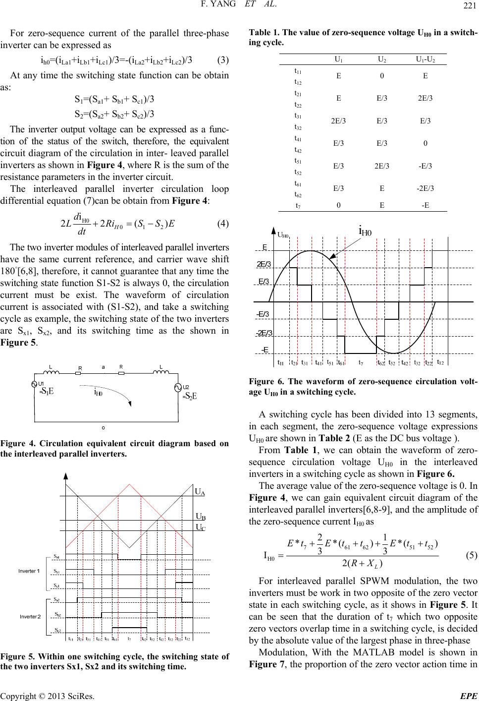 F. YANG ET AL. 221 For zero-sequence current of the parallel three-phase inverter can be expressed as ih0=(iLa1+iLb1+iLc1)/3=-(iLa2+iLb2+iLc2)/3 (3) At any time the switching state function can be obtain as: S1=(Sa1+ Sb1+ Sc1)/3 S2=(Sa2+ Sb2+ Sc2)/3 The inverter output voltage can be expressed as a func- tion of the status of the switch, therefore, the equivalent circuit diagram of the circulation in inter- leaved parallel inverters as shown in Figure 4, where R is the sum of the resistance parameters in the inverter circuit. The interleaved parallel inverter circulation loop differential equation (7)can be obtain from Figure 4: H0 012 i 22( H d LRiSS dt )E (4) The two inverter modules of interleaved parallel inverters have the same current reference, and carrier wave shift 180◦[6,8], therefore, it cannot guarantee that any time the switching state function S1-S2 is always 0, the circulation current must be exist. The waveform of circulation current is associated with (S1-S2), and take a switching cycle as example, the switching state of the two inverters are Sx1, Sx2, and its switching time as the shown in Figure 5. Figure 4. Circulation equivalent circuit diagram based on the interleaved parallel inverters. Figure 5. Within one switching cycle, the switching state of the two inverters Sx1, Sx2 and its switching time. Table 1. The value of zero-sequence voltage UH0 in a switch- ing cycle. U 1 U2 U1-U2 t11 t12 E 0 E t21 t22 E E/3 2E/3 t31 t32 2E/3 E/3 E/3 t41 t42 E/3 E/3 0 t51 t52 E/3 2E/3 -E/3 t61 t62 E/3 E -2E/3 t7 0 E -E Figure 6. The waveform of zero-sequence circulation volt- age UH0 in a switching cycle. A switching cycle has been divided into 13 segments, in each segment, the zero-sequence voltage expressions UH0 are shown in Table 2 (E as the DC bus voltage ). From Table 1, we can obtain the waveform of zero- sequence circulation voltage UH0 in the interleaved inverters in a switching cycle as shown in Figure 6. The average value of the zero-sequence voltage is 0. In Figure 4, we can gain equivalent circuit diagram of the interleaved parallel inverters[6,8-9], and the amplitude of the zero-sequence current IH0 as 76162 51 H0 21 **()*( 33 I2( ) L EtE ttE tt RX 52 ) (5) For interleaved parallel SPWM modulation, the two inverters must be work in two opposite of the zero vector state in each switching cycle, as it shows in Figure 5. It can be seen that the duration of t7 which two opposite zero vectors overlap time in a switching cycle, is decided by the absolute value of the largest phase in three-phase Modulation, With the MATLAB model is shown in Figure 7, the proportion of the zero vector action time in Copyright © 2013 SciRes. EPE 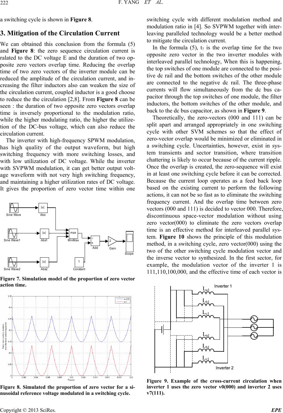 F. YANG ET AL. 222 a switching cycle is shown in Figure 8. 3. Mitigation of the Circulation Current We can obtained this conclusion from the formula (5) and Figure 8: the zero sequence circulation current is ralated to the DC voltage E and the duration of two op- posite zero vectors overlap time. Reducing the overlap time of two zero vectors of the inverter module can be reduced the amplitude of the circulation current, and in- creasing the filter inductors also can weaken the size of the circulation current, coupled inductor is a good choose to reduce the the circulation [2,8]. From Figure 8 can be seen : the duration of two opposite zero vectors overlap time is inversely proportional to the modulation ratio, while the higher modulating ratio, the higher the utilize- tion of the DC-bus voltage, which can also reduce the circulation current. The inverter with high-frequency SPWM modulation, has high quality of the output waveform, but high switching frequency with more switching losses, and with low utilization of DC voltage. While the inverter with SVPWM modulation, it can get better output volt- age waveform with not very high switching frequency, and maintaining a higher utilization rates of DC voltage. It gives the proportion of zero vector time within one Sine Wave2 Sine Wave1 Sine Wave Scope max MinMax 2 Gai n 1 Constant Add |u| Abs2 |u| Abs1 |u| Abs Figure 7. Simulation model of the proportion of zero vector action time. Figure 8. Simulated the proportion of zero vector for a si- nusoidal reference voltage modulated in a switching cycle. switching cycle with different modulation method and modulation ratio in [4]. So SVPWM together with inter- leaving paralleled technology would be a better method to mitigate the circulation current. In the formula (5), t7 is the overlap time for the two opposite zero vector in the two inverter modules with interleaved parallel technology, When this is happening, the top switches of one module are connected to the posi- tive dc rail and the bottom switches of the other module are connected to the negative dc rail. The three-phase currents will flow simultaneously from the dc bus ca- pacitor through the top switches of one module, the filter inductors, the bottom switches of the other module, and back to the dc bus capacitor, as shown in Figure 9. Theoretically, the zero-vectors (000 and 111) can be split apart and arranged appropriately in one switching cycle with other SVM schemes so that the effect of zero-vector overlap would be minimized or eliminated in a switching cycle. Uncertainties, however, exist in sys- tem transients and sector transition, where transition chattering is likely to occur because of the current ripple. Once the overlap is created, the zero-sequence will exist in at least one switching cycle before it can be corrected. Because the current loop operates as a feed back loop based on the existing current to perform the following actions, it can not be so fast as to eliminate the switching frequency current. And the overlap time between zero vectors (000 and 111) is decided to vector 000. Therefore, discontinuous space-vector modulation without using zero vector(000) to eliminate the zero vectors overlap time is an effective method for interleaved parallel sys- tem. Figure 10 shows the principle of this modulation method, in a switching cycle, zero vector(000) using the two of the other switching cycle modulation vector and the inverse vector to synthesized. In the first sector, for example, the modulation vector of the inverter 1 is 111,110,100,000, and the effective time of each vector is Figure 9. Example of the cross-current circulation when inverter 1 uses the zero vector v0(000) and inverter 2 uses v7(111). Copyright © 2013 SciRes. EPE 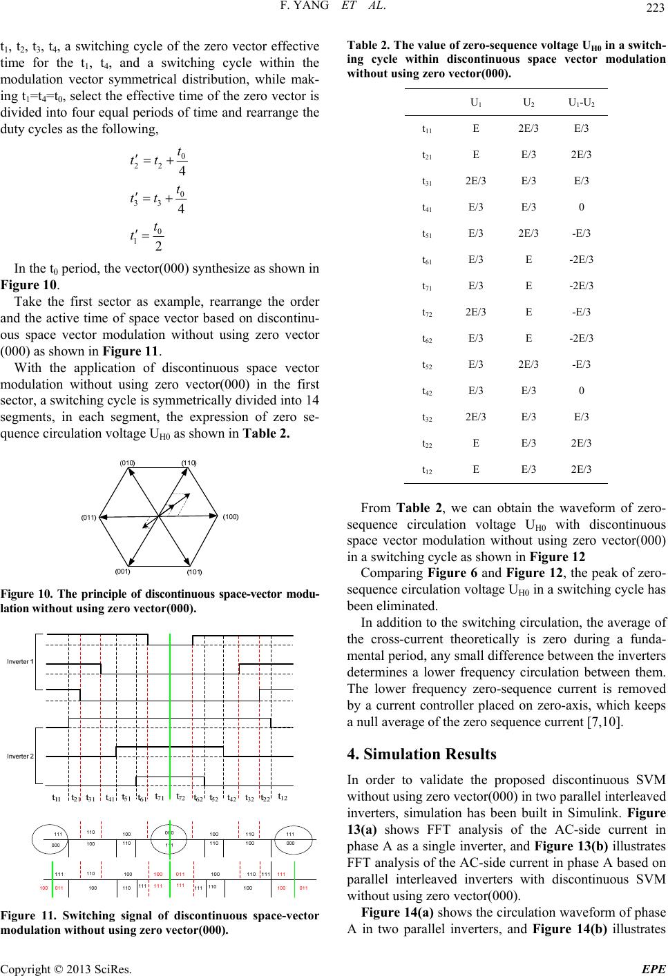 F. YANG ET AL. 223 t1, t2, t3, t4, a switching cycle of the zero vector effective time for the t1, t4, and a switching cycle within the modulation vector symmetrical distribution, while mak- ing t1=t4=t0, select the effective time of the zero vector is divided into four equal periods of time and rearrange the duty cycles as the following, 0 22 0 33 0 1 4 4 2 t tt t tt t t In the t0 period, the vector(000) synthesize as shown in Figure 10. Take the first sector as example, rearrange the order and the active time of space vector based on discontinu- ous space vector modulation without using zero vector (000) as shown in Figure 11. With the application of discontinuous space vector modulation without using zero vector(000) in the first sector, a switching cycle is symmetrically divided into 14 segments, in each segment, the expression of zero se- quence circulation voltage UH0 as shown in Table 2. Figure 10. The principle of discontinuous space-vector modu- lation without using zero vector(000). Figure 11. Switching signal of discontinuous space-vector modulation without using zero vector(000). Table 2. The value of zero-sequence voltage UH0 in a switch- ing cycle within discontinuous space vector modulation without using zero vector(000). U 1 U2 U1-U2 t11 E 2E/3 E/3 t21 E E/3 2E/3 t31 2E/3 E/3 E/3 t41 E/3 E/3 0 t51 E/3 2E/3 -E/3 t61 E/3 E -2E/3 t71 E/3 E -2E/3 t72 2E/3 E -E/3 t62 E/3 E -2E/3 t52 E/3 2E/3 -E/3 t42 E/3 E/3 0 t32 2E/3 E/3 E/3 t22 E E/3 2E/3 t12 E E/3 2E/3 From Table 2, we can obtain the waveform of zero- sequence circulation voltage UH0 with discontinuous space vector modulation without using zero vector(000) in a switching cycle as shown in Figure 12 Comparing Figure 6 and Figure 12, the peak of zero- sequence circulation voltage UH0 in a switching cycle has been eliminated. In addition to the switching circulation, the average of the cross-current theoretically is zero during a funda- mental period, any small difference between the inverters determines a lower frequency circulation between them. The lower frequency zero-sequence current is removed by a current controller placed on zero-axis, which keeps a null average of the zero sequence current [7,10]. 4. Simulation Results In order to validate the proposed discontinuous SVM without using zero vector(000) in two parallel interleaved inverters, simulation has been built in Simulink. Figure 13(a) shows FFT analysis of the AC-side current in phase A as a single inverter, and Figure 13(b) illustrates FFT analysis of the AC-side current in phase A based on parallel interleaved inverters with discontinuous SVM without using zero vector(000). Figure 14(a) shows the circulation waveform of phase A in two parallel inverters, and Figure 14(b) illustrates Copyright © 2013 SciRes. EPE 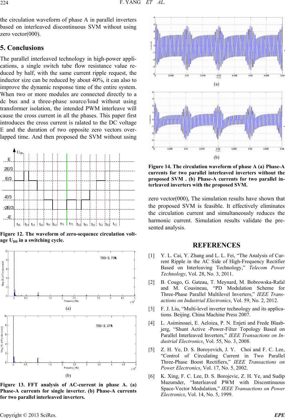 F. YANG ET AL. 224 the circulation waveform of phase A in parallel inverters based on interleaved discontinuous SVM without using zero vector(000). 5. Conclusions The parallel interleaved technology in high-power appli- cations, a single switch tube flow resistance value re- duced by half, with the same current ripple request, the inductor size can be reduced by about 40%, it can also to improve the dynamic response time of the entire system. When two or more modules are connected directly to a dc bus and a three-phase source/load without using transformer isolation, the intended PWM interleave will cause the cross current in all the phases. This paper first introduces the cross current is ralated to the DC voltage E and the duration of two opposite zero vectors over- lapped time. And then proposed the SVM without using Figure 12. The waveform of zero-sequence circulation volt- age UH0 in a switching cycle. (a) (b) Figure 13. FFT analysis of AC-current in phase A. (a) Phase-A currents for single inverter. (b) Phase-A currents for two parallel interleaved inverters. (a) (b) Figure 14. The circulation waveform of phase A (a) Phase-A currents for two parallel interleaved inverters without the proposed SVM . (b) Phase-A currents for two parallel in- terleaved inverters with the proposed SVM. zero vector(000), The simulation results have shown that the proposed SVM is feasible. It effectively eliminates the circulation current and simultaneously reduces the harmonic current. Simulation results validate the pre- sented analysis. REFERENCES [1] Y. L. Cai, Y. Zhang and L. L. Fei, “The Analysis of Cur- rent Ripple in the AC Side of High-Frequency Rectifier Based on Interleaving Technology,” Telecom Power Technology, Vol. 28, No. 3, 2011. [2] B. Cougo, G. Gateau, T. Meynard, M. Bobrowska-Rafal and M. Cousineau, “PD Modulation Scheme for Three-Phase Parallel Multilevel Inverters,” IEEE Trans- actions on Industrial Electronics, Vol. 59, No. 2, 2012. [3] F. J. Liu, “Multi-level inverter technology and its applica- tions. Beijing. China Machine Press 2007. [4] L. Asiminoaei, E. Aeloiza, P. N. Enjeti and Frede Blaab- jerg, “Shunt Active -Power-Filter Topology Based on Parallel Interleaved Inverters,” IEEE Transactions on In- dustrial Electronics, Vol. 55, No. 3, 2008. [5] Z. H. Ye, D. S. Boroyevich, J. Y. Choi and F. C. Lee, “Control of Circulating Current in Two Parallel Three-Phase Boost Rectifiers,” IEEE Transactions on Power Electronics, Vol. 17, No. 5, 2002. [6] K. Xing, F. C. Lee, D. S. Borojevic, Z. H. Ye, and Sudip Mazumder, “Interleaved PWM with Discontinuous Space-Vector Modulation,” IEEE Transactions on Power Electronics, Vol. 14, No. 5, 1999. Copyright © 2013 SciRes. EPE  F. YANG ET AL. Copyright © 2013 SciRes. EPE 225 [7] L. A. Moran, J. W. Dixon and R. R. Wallace, “A Three-phase Active Power Filter Operating with Fixed Switching Frequency for Reactive Power and Current Harmonic Compensation,” IEEE Transactions on Indus- trial Electronics , Vol. 42, No. 4, 1995, pp. 402-408. doi:10.1109/41.402480 [8] P.-W. Lee, Y.-S. Lee, D. K. W. Cheng, and X.-C. Liu, “Steady-state Analysis of an Interleaved Boost Converter with Coupled Inductors,” IEEE Transactions on Indus- trial Electronics, Vol. 47, No. 4, 2000, pp. 787-795. doi:10.1109/41.857959 [9] J. M. Guerrero, L. Garcia de Vicuna, J. Matas, M. Castilla, and J. Miret, “Output Impedance Design of Parallel- Connected UPS Inverters with Wireless Load-sharing Control,” IEEE Transactions on Industrial Electronics, Vol. 52, No. 4, 2005, pp. 1126-1135. doi:10.1109/TIE.2005.851634 [10] Y. H. Zhi, D. Boroyevich, C. Jae-Young and F. C. Lee, “Control of Circulating Current in Two Parallel Three-phase Boost Rectifiers,” IEEE Transactions on Power Electronics, Vol. 17, No. 5,2002, pp. 609-615.doi:10.1109/TPEL.2002.802170
|