J. LIU, Y. G. ZHANG
206
the Micro-controller with some feedback signals from the
circuit, such the DC Bus voltage, the inverter output
voltage and the PLL signal. And the whole control sys-
tem is a close loop with voltage regulation [6].
In order to get high quality output AC voltage, there is
a filter circuit at the terminal of the output of the inverter,
which can filter the high numbers harmonics produced
by the inverter, even though the voltage THD (Total
Harmonic Distortion) is very small with SPWM control
algorithm.
There is a human-machine Interface in PC, which is
communicated with the controller card through SCI (Se-
rial Communication Interface) and programmed with C#
language. The functions of the interface software are to
initialize and set the control parameters of the control
system; setup the control models; monitor the p arameters
get from controller card and give out the sine waveform
of the power grid voltage, voltage waveform of the out-
put of the inverter[7].
With the interface, it is convenience to change the pa-
rameters of control and observe the different results
caused by different parameters. And using the interface
software can give quickly starting to study the control
algorithm and understand the operation principle of PV
power generation system more easily. It is a good assis-
tant to control and monitor the operation of the DC-DC
Boost circuit, PLL circuit and the inverter circuit, and
can store the data of operation in the PC [8].
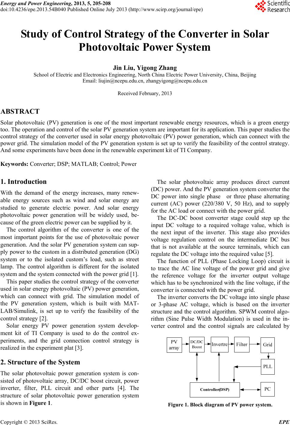
3. Simulation Model
The solar photovoltaic power generation system simula-
tion model is established with the MATLAB/Simulink.
The simulation model structure is shown in Figur e 2.
The PV array produces variable DC voltage according
to the sun light and temperature.
The DC/DC Boost block step up the DC voltage into a
required DC Bus voltage, which is the voltage of the ca-
pacitor in Figure 2. And the DC Bus voltage should
great than the peak value of the AC side voltage if the
active power wants to be transmitted from the DC side to
the AC side [9].
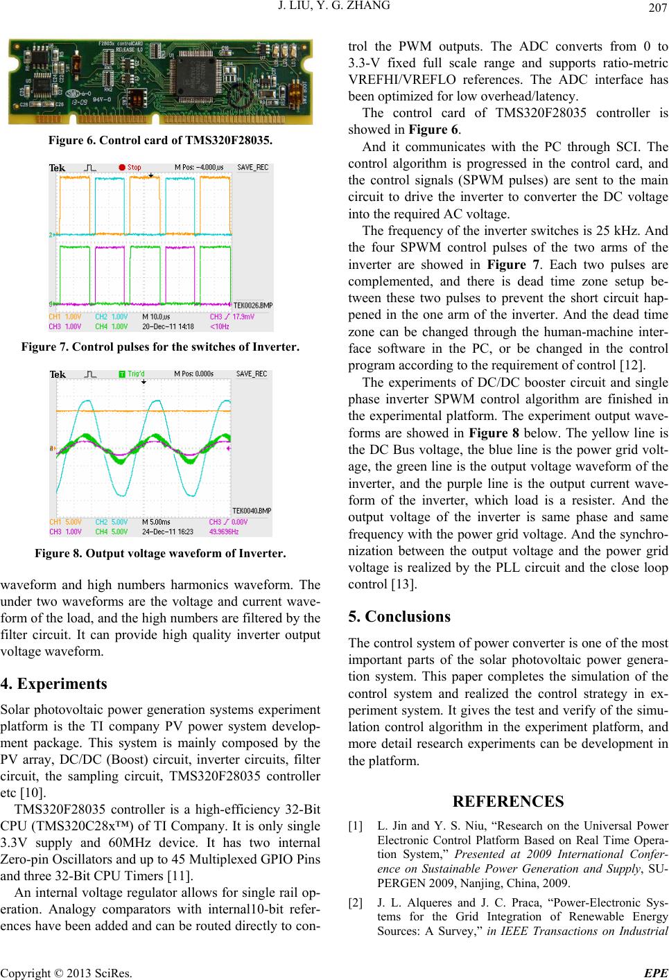
The DC Bus voltage regulation control subsystem
block is showed in Figure 3. It is consisted of PLL block,
abc to dq0 converter block, PI controller block, dq0 to
abc inverter block and the PWM pulses generator block.
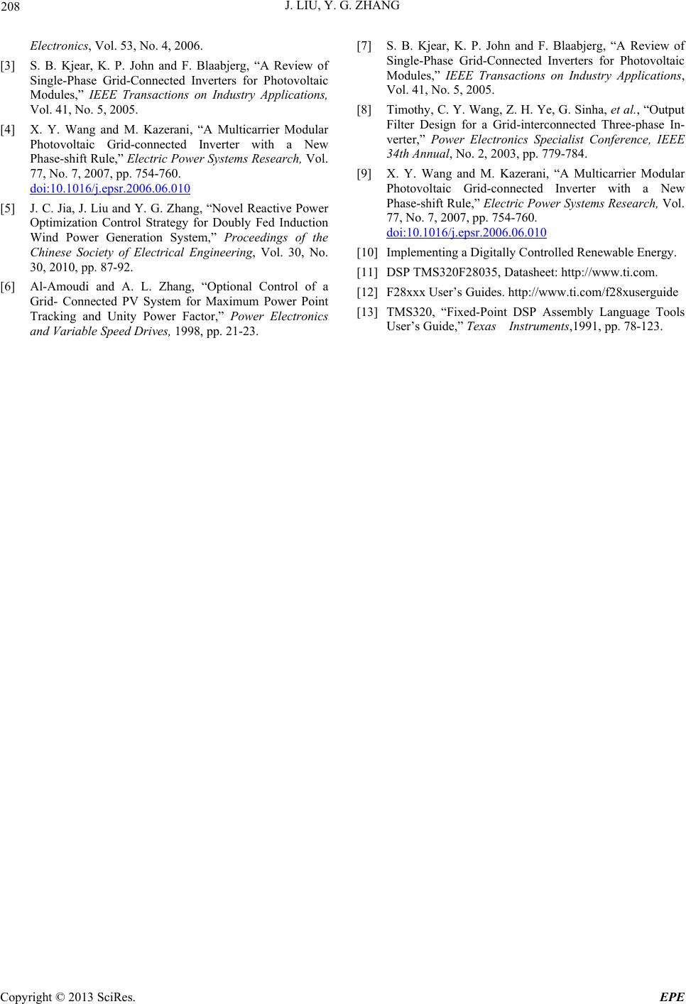
The inverter circuit is a three phase full bridge voltage
source converter, which uses the IGBT as switches, and
there are Diodes reverse parallel connected with the
IGBTs. The function of Diodes is to provide the flow
path for the reactive power flowing from the AC side to
the DC side. SPWM control model is used to generate
the PWM pulses to drive the switches of the inverter and
converter the DC voltage into AC voltage. The SPWM
control pulses for IGBT1 and IGBT2 are showed in Fig-
ure 4. The width of pulse is changed as a sinusoidal
waveform. And the pulses of IGBT1 and IGBT2 are op-
posite because they are connected in one bridge arm. The
dead time of the IGBTs is not considered in the simula-
tion model, which is considered in the reality control
system.
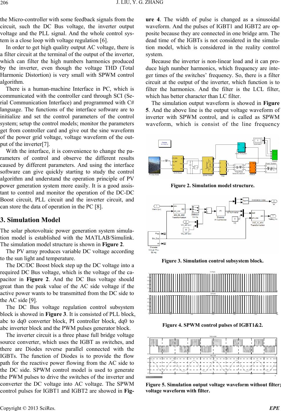
Because the inverter is non-linear load and it can pro-
duce high number harmonics, which frequency are inte-
ger times of the switches’ frequency. So, there is a filter
circuit at the output of the inverter, which function is to
filter the harmonics. And the filter is the LCL filter,
which has better character than LC filter.
The simulation output waveform is showed in Figure
5. And the above line is the output voltage waveform of
inverter with SPWM control, and is called as SPWM
waveform, which is consist of the line frequency
Figure 2. Simulation model structure.
Figure 3. Simulation control subsyste m bloc k.
0
0.2
0.4
0.6
0.8
1
V1-Pusle
00.01 0.02 0.03 0.04 0.05 0.06
0
0.2
0.4
0.6
0.8
1
V2-Pulse
Figure 4. SPWM control pulses of IGBT1&2.
-500
0
500
S
Vab inverter
00.01 0.02 0.03 0.04 0.050.06 0.07 0.08 0.090.1
-400
-200
0
200
400
S
Vab_load
Figure 5. Simulation output voltage waveform without filter;
voltage waveform with fi lter.
Copyright © 2013 SciRes. EPE