Paper Menu >>
Journal Menu >>
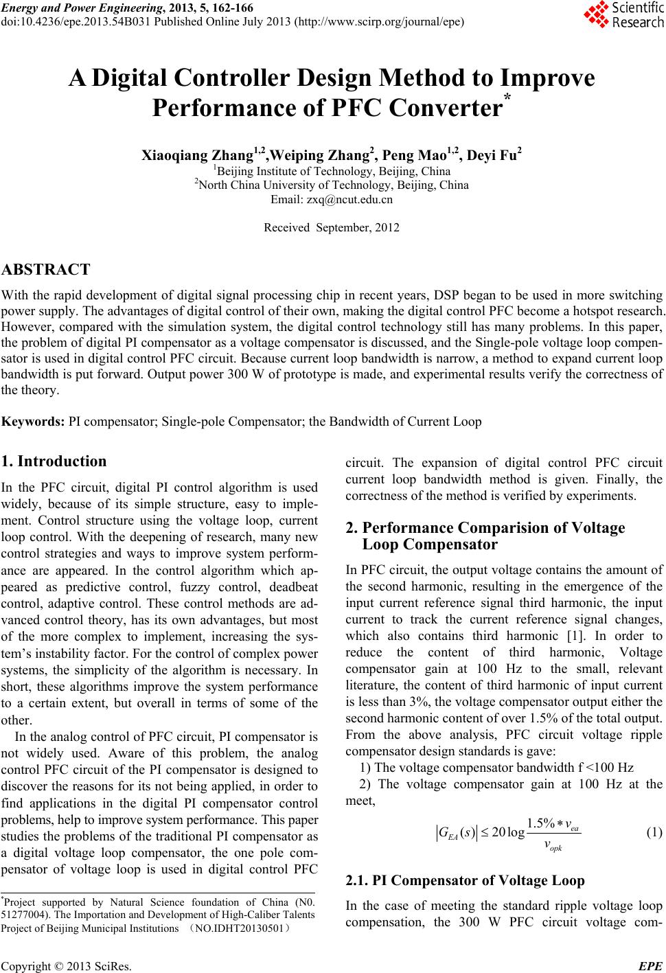 Energy and Power Engineering, 2013, 5, 162-166 doi:10.4236/epe.2013.54B031 Published Online July 2013 (http://www.scirp.org/journal/epe) A Digital Controller Design Method to Improve Performance of PFC Converter* Xiaoqiang Zhang1,2,Weiping Zhang2, Peng Mao 1,2, Deyi Fu2 1Beijing Institute of Technology, Beijing, China 2North China University of Technology, Beijing, China Email: zxq@ncut.edu.cn Received September, 2012 ABSTRACT With the rapid development of digital signal processing chip in recent years, DSP began to be used in more switching power supply. The advantages of digital control of their own, making the digital control PFC become a hotspot research. However, compared with the simulation system, the digital control technology still has many problems. In this paper, the problem of digital PI co mpensator as a voltage compensa tor is discussed, and the Single-pole voltage lo op compen- sator is used in digital control PFC circuit. Because current loop bandwidth is narrow, a method to expand current loop bandwidth is put forward. Output power 300 W of prototype is made, and experimental results verify the correctness of the theory. Keywords: PI compensator; Single-pole Compensator; the Bandwidth of Current Loop 1. Introduction In the PFC circuit, digital PI control algorithm is used widely, because of its simple structure, easy to imple- ment. Control structure using the voltage loop, current loop control. With the deepening of research, many new control strategies and ways to improve system perform- ance are appeared. In the control algorithm which ap- peared as predictive control, fuzzy control, deadbeat control, adaptive control. These control methods are ad- vanced control theory, has its own advantages, but most of the more complex to implement, increasing the sys- tem’s instability factor. For the control of complex power systems, the simplicity of the algorithm is necessary. In short, these algorithms improve the system performance to a certain extent, but overall in terms of some of the other. In the analog control of PFC circuit, PI compensato r is not widely used. Aware of this problem, the analog control PFC circuit of the PI compensator is designed to discover the reasons for its not being applied, in order to find applications in the digital PI compensator control problems, hel p t o improve system performance. This paper studies the problems of the traditio nal PI compensator as a digital voltage loop compensator, the one pole com- pensator of voltage loop is used in digital control PFC circuit. The expansion of digital control PFC circuit current loop bandwidth method is given. Finally, the correctness of the method is verified by experiments. 2. Performance Comparision of Voltage Loop Compensator In PFC circuit, the output voltage contains the amount of the second harmonic, resulting in the emergence of the input current reference signal third harmonic, the input current to track the current reference signal changes, which also contains third harmonic [1]. In order to reduce the content of third harmonic, Voltage compensator gain at 100 Hz to the small, relevant literature, the content of third harmonic of input current is less than 3%, the voltage compensator outpu t either the second harm o n ic content of o ver 1 . 5 % of t he total out put. From the above analysis, PFC circuit voltage ripple compensator design standards is gave: 1) The voltage compensator bandwidth f <100 Hz 2) The voltage compensator gain at 100 Hz at the meet, 1.5% () 20logea EA opk v Gs v (1) 2.1. PI Compensator of Voltage Loop *Project supported by Natural Science foundation of China (N0. 51277004). The Importation and Development of High-Caliber Talents Project of Beijing Municipal Institutions (NO.IDHT20130501) In the case of meeting the standard ripple voltage loop compensation, the 300 W PFC circuit voltage com- Copyright © 2013 SciRes. EPE 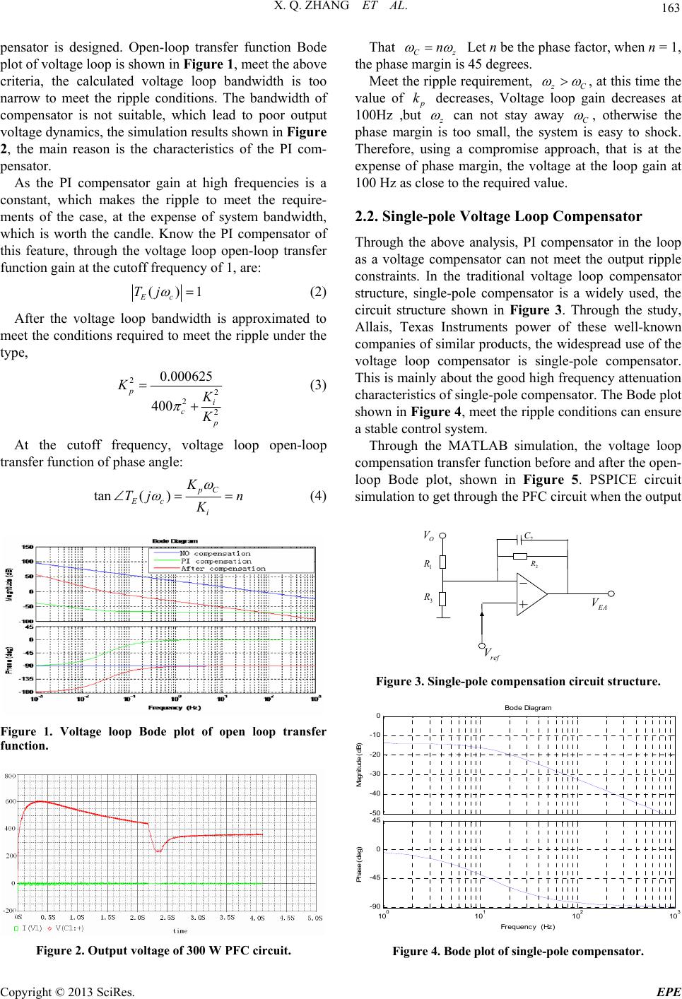 X. Q. ZHANG ET AL. 163 pensator is designed. Open-loop transfer function Bode plot of voltag e loop is sh own in Figure 1, meet the above criteria, the calculated voltage loop bandwidth is too narrow to meet the ripple conditions. The bandwidth of compensator is not suitable, which lead to poor output voltage dynamics, the simulation results shown in Figure 2, the main reason is the characteristics of the PI com- pensator. As the PI compensator gain at high frequencies is a constant, which makes the ripple to meet the require- ments of the case, at the expense of system bandwidth, which is worth the candle. Know the PI compensator of this feature, through the voltage loop open-loop transfer function gain at the cutoff frequency of 1, are: () Ec Tj 1 (2) After the voltage loop bandwidth is approximated to meet the conditions required to meet the ripple under the type, 2 2 22 0.000625 400 p i c p K K K (3) At the cutoff frequency, voltage loop open-loop transfer function of phase angle: tan( )pC Ec i K Tj n K (4) Figure 1. Voltage loop Bode plot of open loop transfer function. Figure 2. Output voltage of 300 W PFC circuit. That Cz n Let n be the phase factor, when n = 1, the phase margin is 45 degrees. Meet the ripple requirement, z C , at this time the value of p k decreases, Voltage loop gain decreases at 100Hz ,but z can not stay away C , otherwise the phase margin is too small, the system is easy to shock. Therefore, using a compromise approach, that is at the expense of phase margin, the voltage at the loop gain at 100 Hz as close to the required value. 2.2. Single-pole Voltage Loop Compensator Through the above analysis, PI compensator in the loop as a voltage compensator can not meet the output ripple constraints. In the traditional voltage loop compensator structure, single-pole compensator is a widely used, the circuit structure shown in Figure 3. Through the study, Allais, Texas Instruments power of these well-known companies of similar products, the widespread use of the voltage loop compensator is single-pole compensator. This is mainly about th e good high frequency attenu ation characteristics of single-pole compensator. The Bode plot shown in Figure 4, meet the ripple conditions can ensu re a stable control system. Through the MATLAB simulation, the voltage loop compensation transfer function before and after the op en- loop Bode plot, shown in Figure 5. PSPICE circuit simulation to get through the PFC circuit when the output 1 R2 R E A V 2 C 3 R ref V O V Figure 3. Single-pole compensation circuit structure. -50 -40 -30 -20 -10 0 Magnitude (dB) 10 0 10 1 10 2 10 3 -90 -45 0 45 Phase (deg) Bode Diagram F requency (Hz) Figure 4. Bode plot of sin g le-pole compensator. Copyright © 2013 SciRes. EPE 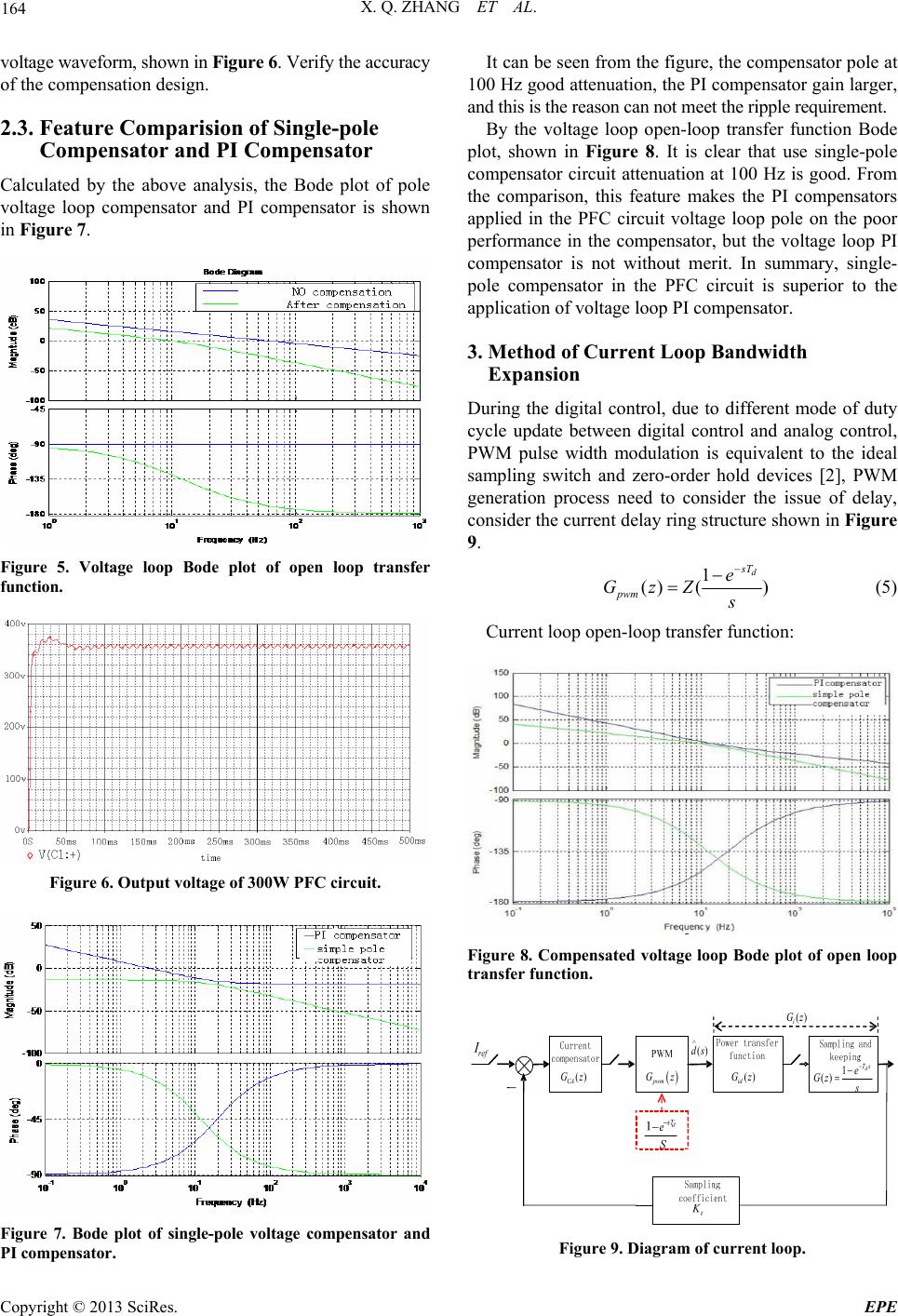 X. Q. ZHANG ET AL. 164 voltage waveform, shown i n Figure 6. Verify the accuracy of the compensation design. 2.3. Feature Comparision of Single-pole Compensator and PI Compensator Calculated by the above analysis, the Bode plot of pole voltage loop compensator and PI compensator is shown in Figure 7. Figure 5. Voltage loop Bode plot of open loop transfer function. Figure 6. Output voltage of 300W PFC circuit. Figure 7. Bode plot of single-pole voltage compensator and PI compensator. It can be seen from the figure, the compensator pole at 100 Hz good attenuation, the PI compensator gain larger, and this is the reason can not meet the ripple requirement. By the voltage loop open-loop transfer function Bode plot, shown in Figure 8. It is clear that use single-pole compensator circuit attenuation at 100 Hz is good. From the comparison, this feature makes the PI compensators applied in the PFC circuit voltage loop pole on the poor performance in the compensator, but the voltage loop PI compensator is not without merit. In summary, single- pole compensator in the PFC circuit is superior to the application of voltage loop PI compensator. 3. Method of Current Loop Bandwidth Expansion During the digital control, due to different mode of duty cycle update between digital control and analog control, PWM pulse width modulation is equivalent to the ideal sampling switch and zero-order hold devices [2], PWM generation process need to consider the issue of delay, consider the current delay ring structure shown in Figure 9. 1 () () d sT pwm e GzZ s (5) Current loop open-loop transfer func tion: Figure 8. Compensated voltage loop Bode plot of open loop transfer function. () CA Gz pwm Gz () id Gz ()ds () i Gz 1 () d Ts e Gz s Figure 9. Diagram of current loop. Copyright © 2013 SciRes. EPE 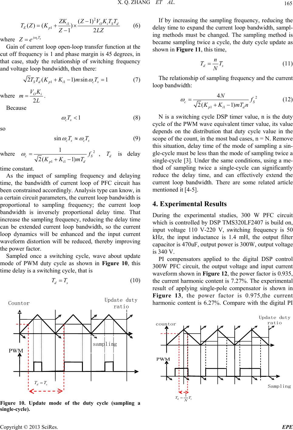 X. Q. ZHANG ET AL. 165 2 1 1(1) () () 12 iOi Ep Sd Z KZVKTT TZ K Z LZ (6) where cs j T Ze Gain of curr ent loop open-loop transf er function at the cut off frequency is 1 and phase margin is 45 degrees, in that case, study the relationship of switching frequency and voltage loop bandwidth, then there: 11 2( 1)sin Sd pics TT KKmT 1 (7) where 2 Oi VK mL . Because 1 cs T (8) so sin cs cs TT (9) where 2 11 1 2( 1) c pi d S f KK mT , ant. s d T is delay time const As the impact of sampling frequency and delaying time, the bandwidth of current loop of PFC circuit has been constrained accordingly. Analysis type can know, in a certain circuit parameters, the current loop bandwidth is proportional to sampling frequency; the current loop bandwidth is inversely proportional delay time. That increase the sampling frequency, reducing the delay time can be extended current loop bandwidth, so the current loop dynamics will be enhanced and the input current waveform distortion will be reduced, thereby improving the power factor. Sampled once a switching cycle, wave about update mode of PWM duty cycle as shown in Figure 10, this time delay is a switching cycle, that is d TT (10) ds TT Figure 10. Update mode of the duty cycle (sampling a single-cycle). If by increasing the sampling frequency, reducing the delay time to expand the current loop bandwidth, sampl- ing methods must be changed. The sampling method is became sampling twice a cycle, the duty cycle update as shown in Figure 11, this time, d n T N s T (11) The relationship of sampling frequency and the current loop bandwidth: 2 11 4 2( 1) cS pi d N f KK mTn (12) N is a switching cycle DSP timer value, n is the duty cycle of the PWM wave equivalent timer value, its value depends on the distribution that duty cycle value in the scope of the count, in the most bad cases, n = N. Remove this situation, delay time of the mode of sampling a sin- gle-cycle must be less than the mode of sampling twice a single-cycle [3]. Under the same conditions, using a me- thod of sampling twice a single-cycle can significantly reduce the delay time, and can effectively extend the current loop bandwidth. There are some related article mentioned it [4-5]. 4. Experimental Results During the experimental studies, 300 W PFC circuit which is controlled by DSP TMS320LF2407 is build on, input voltage 110 V-220 V, switching frequency is 50 kHz, the input inductance is 1.4 mH, the output filter capacitor is 470uF, output power is 300W, output voltage is 340 V. PI compensators applied to the digital DSP control 300W PFC circuit, the output voltage and input current waveform shown in Figure 12, th e po wer f actor is 0.935, the current harmonic content is 7.27%. The experimental result of applying single-pole compensator is shown in Figure 13, the power factor is 0.975,the current harmonic content is 6.27%. Compare with the digital PI d1 s TT N Copyright © 2013 SciRes. EPE 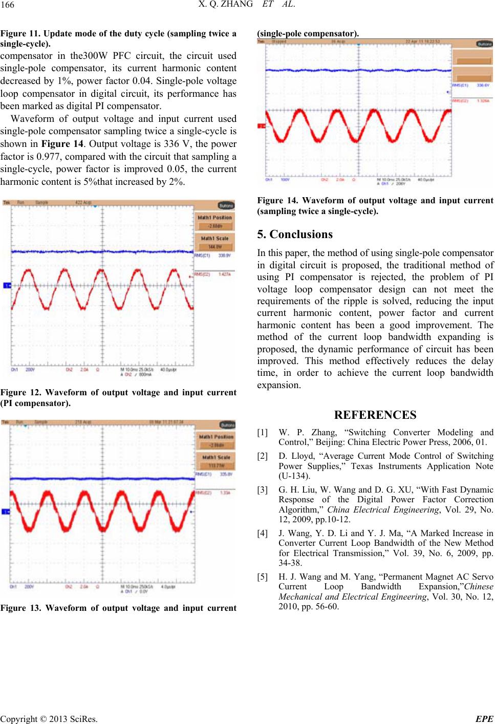 X. Q. ZHANG ET AL. Copyright © 2013 SciRes. EPE 166 Figure 11. Update mode of the duty cycle (samplin g twice a single-cycle). compensator in the300W PFC circuit, the circuit used single-pole compensator, its current harmonic content decreased by 1%, power factor 0.04. Single-pole voltage loop compensator in digital circuit, its performance has been marked as digital PI compensator. Waveform of output voltage and input current used single-pole compensator sampling twice a single-cycle is shown in Figure 14. Output voltage is 336 V, the power factor is 0.977, compared with the circuit that sampling a single-cycle, power factor is improved 0.05, the current harmonic content is 5%that increased by 2%. Figure 12. Waveform of output voltage and input current (PI compensator). Figure 13. Waveform of output voltage and input current (single-pole compensator). Figure 14. Waveform of output voltage and input current (sampling twice a single-cycle). 5. Conclusions In this paper, the method of using single-pole compensator in digital circuit is proposed, the traditional method of using PI compensator is rejected, the problem of PI voltage loop compensator design can not meet the requirements of the ripple is solved, reducing the input current harmonic content, power factor and current harmonic content has been a good improvement. The method of the current loop bandwidth expanding is proposed, the dynamic performance of circuit has been improved. This method effectively reduces the delay time, in order to achieve the current loop bandwidth expansion. REFERENCES [1] W. P. Zhang, “Switching Converter Modeling and Control,” Beijing: China Electric Power Press, 2006, 01. [2] D. Lloyd, “Average Current Mode Control of Switching Power Supplies,” Texas Instruments Application Note (U-134). [3] G. H. Liu, W. Wang and D. G. XU, “With Fast Dynamic Response of the Digital Power Factor Correction Algorithm,” China Electrical Engineering, Vol. 29, No. 12, 2009, pp.10-12. [4] J. Wang, Y. D. Li and Y. J. Ma, “A Marked Increase in Converter Current Loop Bandwidth of the New Method for Electrical Transmission,” Vol. 39, No. 6, 2009, pp. 34-38. [5] H. J. Wang and M. Yang, “Permanent Magnet AC Servo Current Loop Bandwidth Expansion,”Chinese Mechanical and Electrical Engineering, Vol. 30, No. 12, 2010, pp. 56-60. |