Paper Menu >>
Journal Menu >>
 Circuits and Systems, 2011, 2, 18-24 doi:10.4236/cs.2011.21004 Published Online January 2011 (http://www.SciRP.org/journal/cs) Copyright © 2011 SciRes. CS Phase and Quadrature Puls ed Bias LC-CMOS VCO Stefano Perticaroli1, Fabrizio Palma1, Adriano Carbone2 1Department of Information Engineering, Electronics and Telecommunications, Sapienza Università di Roma, Rome, Italy 2Rhea System S. A., Louvain-La-Neuve, Belgium E-mail: perticaroli@die.uniroma1.it Received October 8, 2010; revised October 27, 2010; accepted November 10, 2010 Abstract Pulsed bias is an attempt to improve the performance of oscillators in integrated circuits as a result of archi- tectural innovation. Given the relatively low value of resonator quality factor achievable on-chip, for a speci- fied bias voltage level, pulsed bias may result in a lower power consumption and in an improvement of the spectral purity of the oscillation. The main drawback of this approach is the need to introduce a certain time delay in order to properly position pulses with respect to oscillation waveform. Delay accumulation requires further energy dissipation and introduce additional jitter. In this paper we present a new architecture capable to avoid unnecessary delay, based on the idea to apply the pulsed bias approach to a quadrature oscillator. A first circuit-level implementation of this concept is presented with simulation results. Keywords: Phase And Quadrature VCO, Pulsed Bias Oscillator, Floquet Eigenvectors Noise Decomposition 1. Introduction All the recent theories of phase noise point out the intrin- sic time-varying nature of its generation[1-4]. Ocillators in fact are nonlinear systems with a periodically time- variant steady state. For this reason, internal noise sources, whose variances depend on the operating point, must be described as cyclostationary processes. Furthemore, pe- riodicity implies that also the conversion process of noise sources into phase and orbital deviation is described by a linear periodically time-variant (LPTV) system. Floquet eigenvectors decomposition is widely acknowledged as a correct approach for the analytical treatment of noise sources in such LPTV systems [3]. Following the Floquet decomposition it can be stated that determination of power density spectrum (PDS) of oscillator depends on mean values of noise sources va- riances multiplied by the square of noise sources projec- tions onto the system’s Floquet eigenvectors. In particular, projections onto the “first eigenvector”, i. e. the vector tangent to the space state orbit, are indicated as the main contributors to the PDS close to the fundamental [5]. In order to obtain a higher spectral purity, the men- tioned mean values should be minimized. This result may be achieved if noise sources are allowed to enter the sys- tem only when their projections onto eigenvectors are possibly around a minimum. Since noise in integrated circuits is due mainly to active devices, we may search for architectures that switch on bias currents, and thus add noise, only in certain time intervals during the oscillation period. These time intervals should be chosen to obtain a minimum of the projection onto eigenvectors. We notice that, in a single VCO this i mplies the need for a circuitry which produces a delay between a threshold crossing and the switching of devices: Additional noise is then intro- duced as jitter in accumulation of delay time. Uncertainty related to this jitter affects th e time instant when th e large current needed to sustain oscillations is provided. For this reason, jitter can be not negligible and may overwhelm any improvem ent obt ai ned t h rou gh p ul sed b i asi ng. In this paper we present a new architecture based on the idea to apply the pulsed bias approach to a quadrature oscillator including two resonators. In particular we pro- pose to adopt a threshold at zero differential voltage of one resonator and apply the consequent pulse, with no delay, at the second one, taking advantage of the natural phase relationship between the zero and the maximum in quadrature signals. Quadrature VCOs are fundamental components in ma- ny RF transceiver systems. Especially when low-IF or direct conversion architecture is required, the generation of two periodic signal in quadrature of phase is a critical issue. One of the main problems with quadrature oscilla- tors, obtained clo s ing in a loop two identical resonators, is 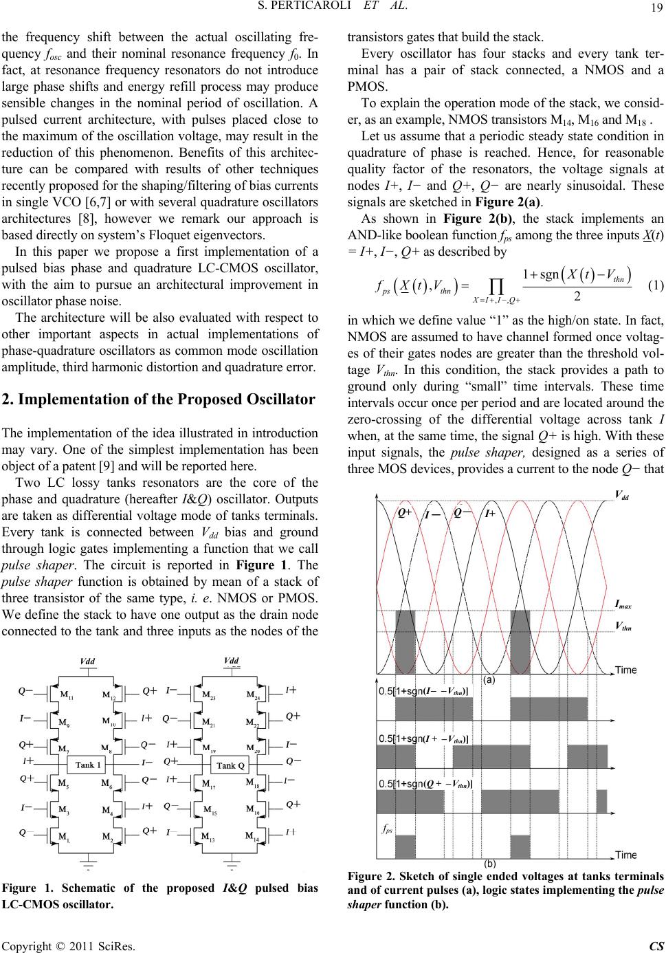 S. PERTICAROLI ET AL. Copyright © 2011 SciRes. CS 19 the frequency shift between the actual oscillating fre- quency fosc and their nominal resonance frequency f0. In fact, at resonance frequency resonators do not introduce large phase shifts and energy refill process may produce sensible changes in the nominal period of oscillation. A pulsed current architecture, with pulses placed close to the maximum of the oscillation voltage, may result in the reduction of this phenomenon. Benefits of this architec- ture can be compared with results of other techniques recently proposed for the shaping/filtering of bias currents in single VCO [6,7] or with several quadrature oscillato rs architectures [8], however we remark our approach is based directly on syst em’s Floquet eigenvec t ors. In this paper we propose a first implementation of a pulsed bias phase and quadrature LC-CMOS oscillator, with the aim to pursue an architectural improvement in oscillator phase noise. The architecture will be also evaluated with respect to other important aspects in actual implementations of phase-quadrature oscillators as common mode oscillation amplitude, t hi rd harmonic distorti on and q uadrature error. 2. Implementation of the Proposed Oscillator The implementation of the idea illustrated in introduction may vary. One of the simplest implementation has been object of a patent [9] and will be reported here. Two LC lossy tanks resonators are the core of the phase and quadrature (hereafter I&Q) oscillator. Outputs are taken as differential voltage mode of tanks terminals. Every tank is connected between Vdd bias and ground through logic gates implementing a function that we call pulse shaper. The circuit is reported in Figure 1. The pulse shaper function is obtained by mean of a stack of three transistor of the same type, i. e. NMOS or PMOS. We define the stack to have one output as the drain node connected to the tank and three inputs as the nodes of the Figure 1. Schematic of the proposed I&Q pulsed bias LC-CMOS oscillator. transistors gates that build the stack. Every oscillator has four stacks and every tank ter- minal has a pair of stack connected, a NMOS and a PMOS. To explain the operation mode of the stack, we consid- er, as an example, NMOS transistors M14, M 16 and M 18 . Let us assume that a periodic steady state cond ition in quadrature of phase is reached. Hence, for reasonable quality factor of the resonators, the voltage signals at nodes I+, I− and Q+, Q− are nearly sinusoidal. These signals are sketched in Figure 2(a). As shown in Figure 2(b), the stack implements an AND-like boolean function fps among the three inputs X(t) = I+, I−, Q+ as described by ,, 1sgn ,2 thn ps thn XII Q Xt V fXtV (1) in which we define value “1” as the high/on state. In fact, NMOS are assumed to have channel formed once voltag- es of their gates nodes are greater than the threshold vol- tage Vthn. In this condition, the stack provides a path to ground only during “small” time intervals. These time intervals occur once per period and are located around the zero-crossing of the differential voltage across tank I when, at the same time, the signal Q+ is high. With these input signals, the pulse shaper, designed as a series of three MOS devices, provides a current to the node Q− that V thn Figure 2. Sketch of single ended voltages at tanks terminals and of current pulses (a), logic states implementing the pulse shaper function (b). Q+ I - Q- I + Vdd Vdd (I- -Vthn)] (I + -Vthn)] (Q + -Vthn)] fps Vdd I max Vthn 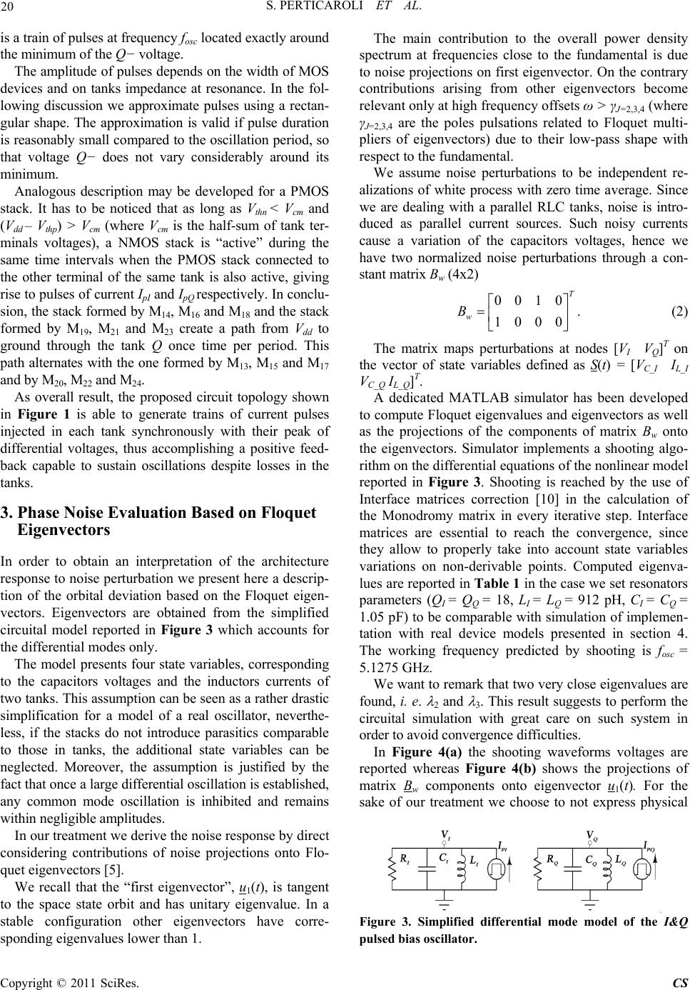 S. PERTICAROLI ET AL. Copyright © 2011 SciRes. CS 20 is a train of pulses at frequency fosc located exactly around the minimum of the Q− voltage. The amplitude of pulses depends on the width of MOS devices and on tanks impedance at resonance. In the fol- lowing discussion we approximate pulses using a rectan- gular shape. The approximation is valid if pulse duration is reasonably small compared to th e oscillation p eriod, so that voltage Q− does not vary considerably around its minimum. Analogous description may be developed for a PMOS stack. It has to be noticed that as long as Vthn < Vcm and (Vdd – Vthp) > Vcm (where Vcm is the half-sum of tank ter- minals voltages), a NMOS stack is “active” during the same time intervals when the PMOS stack connected to the other terminal of the same tank is also active, giving rise to pulses of current IpI and IpQ respectively. In conclu- sion, the stack formed by M14, M16 and M18 and the stack formed by M19, M21 and M23 create a path from Vdd to ground through the tank Q once time per period. This path alternates with the one formed by M13, M15 and M17 and by M20, M22 and M24. As overall result, the proposed circuit topology shown in Figure 1 is able to generate trains of current pulses injected in each tank synchronously with their peak of differential voltages, thus accomplishing a positive feed- back capable to sustain oscillations despite losses in the tanks. 3. Phase Noise Evaluation Based on Floquet Eigenvectors In order to obtain an interpretation of the architecture response to noise perturbatio n we present here a descrip- tion of the orbital deviation based on the Floquet eigen- vectors. Eigenvectors are obtained from the simplified circuital model reported in Figure 3 which accounts for the differential modes only. The model presents four state variables, corresponding to the capacitors voltages and the inductors currents of two tanks. This assumption can be seen as a rather drastic simplification for a model of a real oscillator, neverthe- less, if the stacks do not introduce parasitics comparable to those in tanks, the additional state variables can be neglected. Moreover, the assumption is justified by the fact that once a large differential oscillation is established, any common mode oscillation is inhibited and remains within negligible amplitudes. In our treatment we derive the noise response by direct considering contributions of noise projections onto Flo- quet eigenvectors [5]. We recall that the “first eigenvector”, u1(t), is tangent to the space state orbit and has unitary eigenvalue. In a stable configuration other eigenvectors have corre- sponding eigenvalues lower than 1. The main contribution to the overall power density spectrum at frequencies close to the fundamental is due to noise projectio ns on first eigenvector. On the contrar y contributions arising from other eigenvectors become relevant only at high frequency offsets ω > γJ=2,3,4 (where γJ=2,3,4 are the poles pulsations related to Floquet multi- pliers of eigenvectors) due to their low-pass shape with respect to the fundamental. We assume noise perturbations to be independent re- alizations of white process with zero time average. Since we are dealing with a parallel RLC tanks, noise is intro- duced as parallel current sources. Such noisy currents cause a variation of the capacitors voltages, hence we have two normalized noise perturbations through a con- stant matrix Bw (4x2) 0010 1000 T w B . (2) The matrix maps perturbations at nodes [VI V Q]T on the vector of state variables defined as S(t) = [VC_I I L_I VC_Q IL_Q]T. A dedicated MATLAB simulator has been developed to compute Floquet eigenvalues and eigenvectors as well as the projections of the components of matrix Bw onto the eigenvectors. Simulator implements a shooting algo- rithm on the differential equations of the nonlinear model reported in Figure 3. Shooting is reached by the use of Interface matrices correction [10] in the calculation of the Monodromy matrix in every iterative step. Interface matrices are essential to reach the convergence, since they allow to properly take into account state variables variations on non-derivable points. Computed eigenva- lues are reported in Table 1 in the case we set resonators parameters (QI = QQ = 18, LI = LQ = 912 pH, CI = CQ = 1.05 pF) to be comparable with simulation of implemen- tation with real device models presented in section 4. The working frequency predicted by shooting is fosc = 5.1275 GHz. We want to remark that two very close eigenvalues are found, i. e. 2 and 3. This result suggests to perform the circuital simulation with great care on such system in order to avoid convergence difficulties. In Figure 4(a) the shooting waveforms voltages are reported whereas Figure 4(b) shows the projections of matrix Bw components onto eigenvector u1(t). For the sake of our treatment we choose to not express physical Figure 3. Simplified differential mode model of the I&Q pulsed bias oscillator.  S. PERTICAROLI ET AL. Copyright © 2011 SciRes. CS 21 Table 1. Floquet eigenvalues of I&Q oscillator. 1 2 3 4 1.0039 0.8422 0.8396 0.6991 00.2 0.4 0.6 0.811.2 1.4 1.6 1.82 − 4 − 3 − 2 − 1 0 1 2 3 4 a) (a) 0 0 .2 0 .4 0 . 6 0 . 8 11.2 1.4 1. 6 1. 8 2 8 6 4 2 0 2 4 ) (b) Figure 4. (a) Shooting voltage waveforms of VI (continue trace) and VQ (dashed trace) and (b) simulated projections of [1 0 0 0]T (continue trace) and [0 0 1 0]T (dashed trace) noise vectors onto first Floquet eigenvector. dimensions of projections since they could appear mea- ningless. Eigenvectors, in fact, give a representation in a transformed space, then projections on eigenvectors need to be reconverted into the original space before they can be expressed as voltages or currents. We notice that the projections are around the zero crossing in correspondence of the current pulse on their relative voltage waveforms ([1 0 0 0]T for VI and [0 0 1 0]T for VQ), ensuring minimization of the noise distribu- tion close to the fundamental. Additional relevant behav- iour can be fo und in the li mited increase of the maximum value of the projection. This maximum could greatly in- crease in case the other eigenvectors become non or- thogonal to the first eigenvect or, an d en hance the effect of a noise present all along the orbit, e.g. the noise due to parasitic resistance of the tanks. In conclusion, the model indicates that the architecture appears to be suitable in reduction of both the effect of noise due to bias current and to parasitic resistance. In addition, since the architecture does not require change to position of the pulse, a delay is not required. This further reduces the unavoidable jitter noise introduced by stacks of transistors. 4. Simulation Results Very accurate circuit simulations, including all the se- cond order effects that were previously discarded, have been performed using the SpectreRF simulator within CADENCE IC5.1.41 environment. Devices models are taken from ST 0.13µm technology library. In the following, results obtained for two different configurations at layout versus schematic (LVS) level are reported. Both configurations reflect schematics in Fig- ure 1 but the first configuration consists of fixed tanks whereas varactors are introduced in the second one to build a VCO. We choose to set the working frequency in the 4-5 GHz range. We define as Wint the width of the stack transistor which is connected to the tank, whereas Wmid is related to the median transistor and finally Wext is related to the transistor connected to the voltage supply. Transistors widths of both NMOS and PMOS stacks are chosen as follows: Wint = 85 m, Wmid = 0.5 Wint and Wext = 0.3 Wint with a total number of 8 fingers. In the first configuration the tank is constituted by an octagonal spiral inductor ind_sym_la of 912 pH bundled in the RF ST design kit and a capacitor of 1pF to form a parallel resonator. Inductor has 500 m external diameter and exhibits a qu ality factor Q peak of approximately 18 around 4.5 GHz. A differential amplitude of oscillation of 3.08 V at fosc = 4.77 GHz has been obtained from a biasing of 1.8 V. The total power consumption is about Pdiss= 6.5 mW. Noise level at 3 MHz offset from the fundamental is L{3 MHz} = −147 dBC. In order to com- pare these results with literature ones, relative to oscilla- tors working at different frequencies, with different bi- asing voltages and tank quality factors, the following Figure of Merit (FoM) is used: 1010 1mW 20log 10log osc diss f FoML ffP (3) The resulting FoM for this configuration is equal to 202. Other results of interest are summarized in Table 2. As stated in introduction, the proposed approach can be compared with other bias current shaping techniques also if, at the knowledge of the authors, they have been used in single oscillators rather than in I&Q ones. Both techniques foun d in [6,7] are based on the suppression of  S. PERTICAROLI ET AL. Copyright © 2011 SciRes. CS 22 Table 2. Main characteristics of proposed oscillator. Frequency 4.77 GHz Differential mode amplitude 3.08 V Phase Noise @ 3 MHz offset −147 dBC Power consumption @ 1.8 V supply 6.53 mW FoM as in (3) 202 Quadrature phase error 0.03° Common mode amplitude @ 2fosc 37 mV HD3 −40.4 dB devices noise injected at 2fosc. Since architectures of [6,7] require a tail current source, noise around second har- monic is down-converted to the fundamental, thus in- creasing phase noise. In [6] an LC filter is considered whereas in [7] a phase displacement of pulsed current at 2fosc is used to reduce the down-conversion phenomenon. In the proposed architecture instead there is no need of a tail current source and pulsed biasing currents flow at fundamental frequency. Results of comparison are re- ported in Table 3. For the second configuration a parallel branch is added to the tanks. The branch is constituted of two varactors in series and the control voltage VCTRL is the common node in the series. The total area occupied by varactors is 20 m2. In Figure 5 transient waveforms are reported from postlayout simulation in case fosc = 4.63 GHz for Vctrl = 1.5 V. Periodic steady state occurs in about 10ns without any startup circuitry. A 600 mV difference in amplitude between the two differential voltage modes I and Q is observed, however quadrature of signals is maintained . A close-up of pulsed currents bias is also reported. It has to be noticed that these current waveforms result both from displacement of parasitics as well as form conduction in devices, since a single component cannot be isolated. Moreover, when the peak of a pulse is expected, devices of stack are pushed into triode region by the tank termin- al voltage, giving rise to deformation of the pulse itself. The obtained tuning range with the above mentioned varactors dimensions is about 300 MHz around 4.55 GHz, i. e. 7% relative tenability, and allows the comparison of the proposed architecture with recent literature works as shown in Table 4 Comparison is based on largely adopted PTFN defined as max min 10 10 20log10log B diss ff KT PTFNL ffP (4) Table 3. Comparison with phase noise reduction tech- niques. Ref. L{ f}@3 MHz [dBc] Frequency [GHz] Power consumption [mW] FOM [6] −153 1.2 9.25 195 [7] −135 1.77 2.25 186 This work −147 4.77 6.53 202 Table 4. Comparison with literature I&Q VCO. Ref.Technology [m] Tuning range [GHz] Power consumption [mW] PTFN [11]0.25 1.73−1.99 20 −2.44 [12]0.18 5.4−6.6 18 −1.84 [13]0.25 4.07−4.72 15 −3.17 This work 0.13 4.3−4.64 14 −4.36 (a)  S. PERTICAROLI ET AL. Copyright © 2011 SciRes. CS 23 (b) (c) Figure 5. (a) Transient of tanks differential voltages at startup, (b) signals in quadrature of phase at PSS and (c) close-up of pulsed currents bias of two PMOS and NMOS stacks with respect to differential voltage of tank Q. where fmax − fmin is VCO tuning range, f is offset from fu- ndamental, KB is the Boltzmann constant and T is the absolute temperature. 5. Concluding Remarks In this paper the pulsed bias phase and quadrature oscil- lator has been introduced as an architectural solution for phase noise reduction. The discussion of noise response of the proposed architecture has been based on the eval- uation of noise projections onto the first Floquet eigen- vector of the system. Simulations of the pulsed bias I&Q oscillator and VCO implemented in ST 0.13 µm tech- nology appear to validate noise analysis. Result of this work in comparison with other phase noise reduction techniques as well as with recent measurements of pro- totypes is promising and encourages a real implementa- tion of the described I&Q pulsed bias architecture. 6. References [1] F. X. Kaertner, “Analysis of White and f− Noise in Oscillators,” Inernational Journal of Circuit Theory and Applications, Vol. 18, No. 5, 1990, pp. 485-519. doi:10. 1002/cta.4490180505  S. PERTICAROLI ET AL. Copyright © 2011 SciRes. CS 24 [2] A. Hajimiri and T. H. Lee, “A General Theory of Phase Noise in Electrical Oscillators,” IEEE Journal Solid-State Circuits, Vol. 33, No. 2, 1998, pp. 179-194. doi:10.1109 /4.658619 [3] A. Demir, “Floquet Theory and Non-linear Perturbation Analysis Foroscillators with Differential-Algebraic Eq- uations,” International Journal of Circuit and Theory Applications, Vol. 28, No. 2, 2000, pp. 163-185. doi: 10.1002/(SICI)1097007X(200003/04)28:2<163::AID-CT A101>3.0.CO;2-K [4] A. Carbone, A. Brambilla and F. Palma, “Using Floquet Eigenvectors in the Design of Electronic Oscillators,” Em- erging Technologies: Circuits and Systems for 4 G Mo- bile Wireless Communications, No. 6, 23-24 June 2005, pp. 100-103. [5] A. Carbone and F. Palma, “Considering Orbital Devia- tions on the Evaluation of Power Density Spectrum of Oscill-Ators,” IEEE Transactions on Circuits and Systems-II: Express Briefs, Vol. 53, No. 6, 2006, pp. 438-442. doi: 10.1109/TCSII.2006.873527 [6] E. Hegazi, H. Sjoland and A. Abidi, “A Filtering Tech- nique to Lower LC Oscillator Phase Noise,” IEEE Journal of Solid State Circuits, Vol. 36, No. 12, 2001, pp. 1921- 1930. doi:10.1109/4.972142 [7] B. Soltanian and P. Kinget, “Tail Current Shaping to Improve Phase Noise in LC Voltage Controlled Os- cillators,” IEEE Journal of Solid State Circuits, Vol. 41, No. 8, 2006, pp. 1792-1802. doi:10.1109/JSSC.2006.8772 73 [8] L. B. Oliveira et al., “Analysis and Design of Quadrature Oscillators,” Springer, Berlin, 2008. do i: 10 .1007/978-14020- 8516-1. [9] United States Patent No. US 2008/0218280 A1. [10] A. Carbone and F. Palma, “Discontinuity Correction in Piece-Wise-Linear Models of Oscillators for Phase Noise Characterization,” International Journal of Circuit Theory and Applications, Vol. 35, No. 1, 2007, pp. 93-104. doi:10. 1002/cta.383 [11] M. Tiebout, “A Differentially Tuned Quadrature CMOS,” Proceedings of the 26th European Solid-State Circuits Conference, Montreux, 18-22 September 2006. [12] J. H. Chang, et al., “A New 6 GHz Fully Integrated Low Power Low Phase Noise LC Quadrature VCO,” Pro- ceedings of 2003 Radio Frequency Integrated Circuits Symposium Philadelphia, Philadelphia, 8-10 June 2003, pp. 295-298. [13] F. Yang et al., “A 4.8 GHz CMOS LC Balanced Oscillator with Symmetry Noise Filtering Technique,” International Conference on Solid-State Integrated Circuits Technology, Vol. 2, No. 7, 2004, pp. 1315-1320. doi:10.1109/ICSICT. 2004.1436795 |