Paper Menu >>
Journal Menu >>
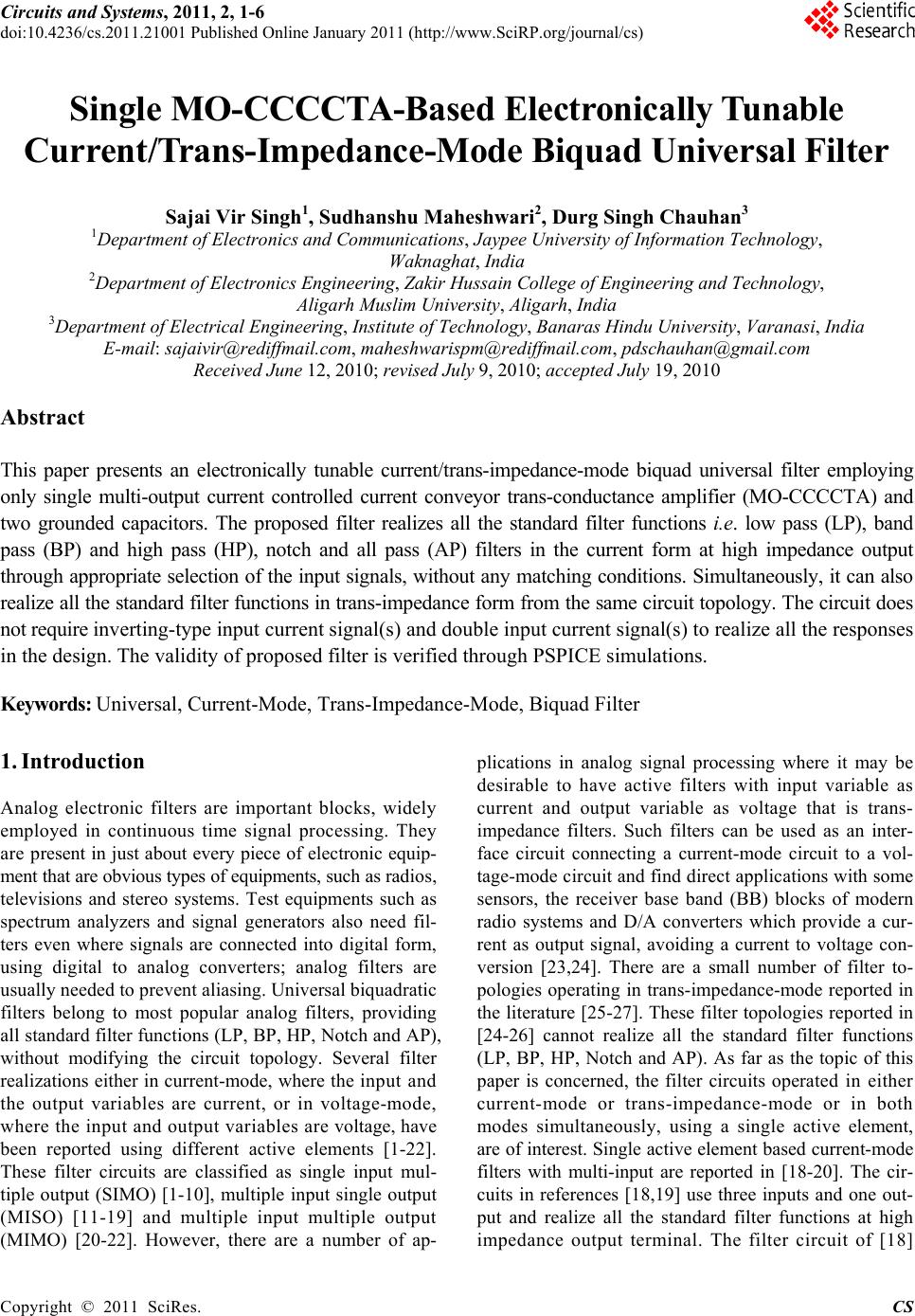 Circuits and Systems, 2011, 2, 1-6 doi:10.4236/cs.2011.21001 Published Online January 2011 (http://www.SciRP.org/journal/cs) Copyright © 2011 SciRes. CS Single MO-CCCCTA-Based Electr onically Tunable Curr ent/Tr ans-Impedance-Mode Biquad Universal Filter Sajai Vir Singh1, Sudhanshu Maheshwari2, Durg Singh Chauhan3 1Department of Electronics and Communications, Jaypee University of Information Technology, Waknaghat, India 2Department of Electronics Engineering, Zakir Hussain College of Engineering and Technology, Aligarh Muslim University, Aligarh, India 3Department of Electrical Engineering, Institute of Technology, Banaras Hindu University, Varanasi, India E-mail: sajaivir@rediffmail.com, maheshwarispm@rediffmail.com, pdschauhan@gmail.com Received June 12, 2010; revised July 9, 2010; accepted July 19, 2010 Abstract This paper presents an electronically tunable current/trans-impedance-mode biquad universal filter employing only single multi-output current controlled current conveyor trans-conductance amplifier (MO-CCCCTA) and two grounded capacitors. The proposed filter realizes all the standard filter functions i.e. low pass (LP), band pass (BP) and high pass (HP), notch and all pass (AP) filters in the current form at high impedance output through appropriate selection of the input signals, without any matching conditions. Simultaneously, it can also realize all the standard filter functions in trans-impedance form from the same circuit topology. The circuit does not require inverting-type input current signal(s) and double input current signal(s) to realize all the responses in the design. The validity of proposed filter is verified through PSPICE simulations. Keywords: Universal, Current-Mode, Trans-Impedance-Mode, Biquad Filter 1. Introduction Analog electronic filters are important blocks, widely employed in continuous time signal processing. They are present in just about every piece of electronic equip- ment that are obvious types of equipments, such as radios, televisions and stereo systems. Test equipments such as spectrum analyzers and signal generators also need fil- ters even where signals are connected into digital form, using digital to analog converters; analog filters are usually needed to prevent aliasing. Universal biquadratic filters belong to most popular analog filters, providing all standard filter functions (LP, BP, HP, Notch and AP), without modifying the circuit topology. Several filter realizations either in current-mode, where the input and the output variables are current, or in voltage-mode, where the input and output variables are voltage, have been reported using different active elements [1-22]. These filter circuits are classified as single input mul- tiple output (SIMO) [1-10], multiple input single output (MISO) [11-19] and multiple input multiple output (MIMO) [20-22]. However, there are a number of ap- plications in analog signal processing where it may be desirable to have active filters with input variable as current and output variable as voltage that is trans- impedance filters. Such filters can be used as an inter- face circuit connecting a current-mode circuit to a vol- tage-mode circuit and find direct applications with some sensors, the receiver base band (BB) blocks of modern radio systems and D/A converters which provide a cur- rent as output signal, avoiding a current to voltage con- version [23,24]. There are a small number of filter to- pologies operating in trans-impedance-mode reported in the literature [25-27]. These filter topologies reported in [24-26] cannot realize all the standard filter functions (LP, BP, HP, Notch and AP). As far as the topic of this paper is concerned, the filter circuits operated in either current-mode or trans-impedance-mode or in both modes simultaneously, using a single active element, are of interest. Single active element based current-mode filters with multi-input are reported in [18-20]. The cir- cuits in references [18,19] use three inputs and one out- put and realize all the standard filter functions at high impedance output terminal. The filter circuit of [18] 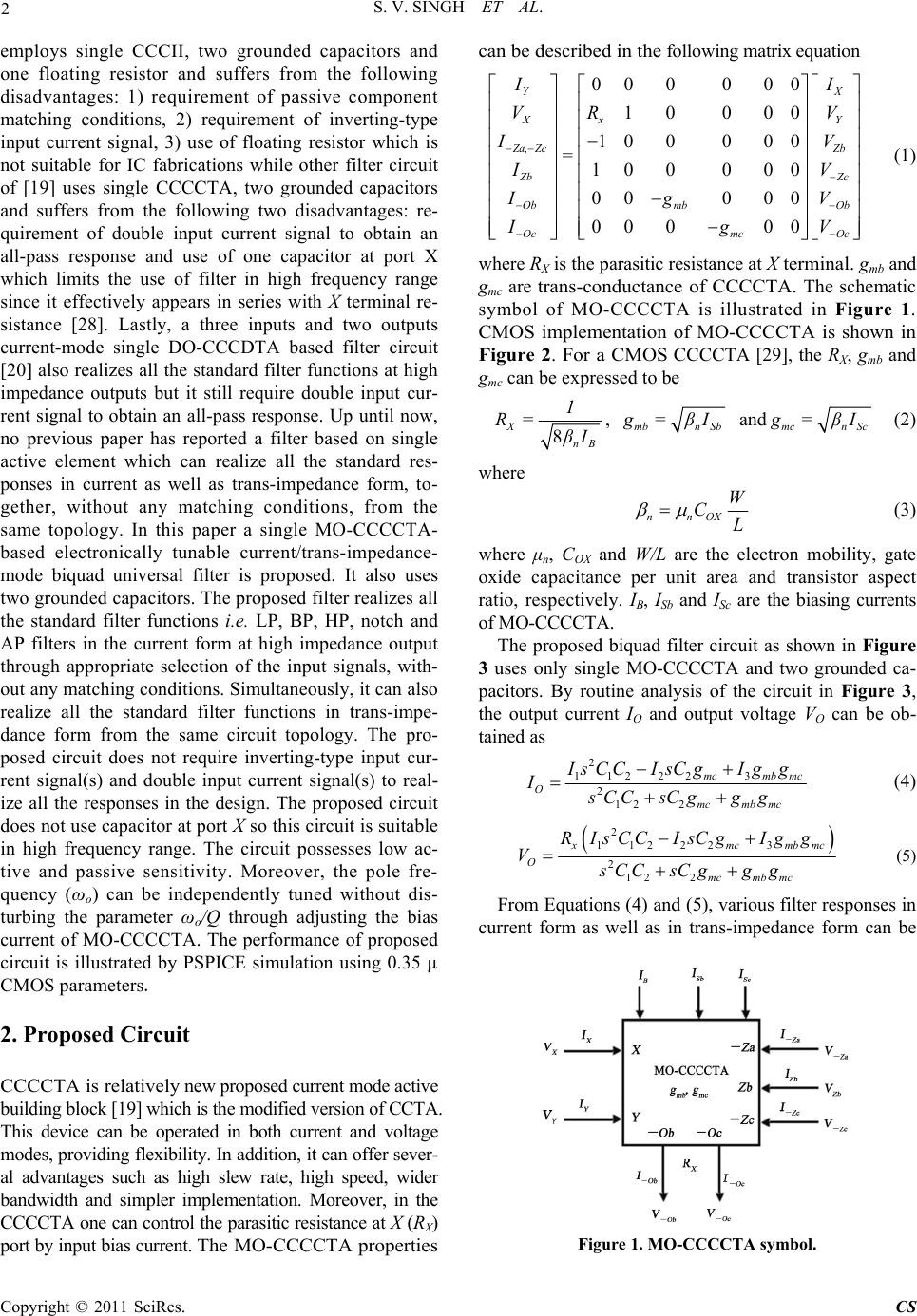 S. V. SINGH ET AL. Copyright © 2011 SciRes. CS 2 employs single CCCII, two grounded capacitors and one floating resistor and suffers from the following disadvantages: 1) requirement of passive component matching conditions, 2) requirement of inverting-type input current signal, 3) use of floating resistor which is not suitable for IC fabrications while other filter circuit of [19] uses single CCCCTA, two grounded capacitors and suffers from the following two disadvantages: re- quirement of double input current signal to obtain an all-pass response and use of one capacitor at port X which limits the use of filter in high frequency range since it effectively appears in series with X terminal re- sistance [28]. Lastly, a three inputs and two outputs current-mode single DO-CCCDTA based filter circuit [20] also realizes all the standard filter functions at high impedance outputs but it still require double input cur- rent signal to obtain an all-pass response. Up until now, no previous paper has reported a filter based on single active element which can realize all the standard res- ponses in current as well as trans-impedance form, to- gether, without any matching conditions, from the same topology. In this paper a single MO-CCCCTA- based electronically tunable current/trans-impedance- mode biquad universal filter is proposed. It also uses two grounded capacitors. The proposed filter realizes all the standard filter functions i.e. LP, BP, HP, notch and AP filters in the current form at high impedance output through appropriate selection of the input signals, with- out any matching conditions. Simultaneously, it can also realize all the standard filter functions in trans-impe- dance form from the same circuit topology. The pro- posed circuit does not require inverting-type input cur- rent signal(s) and double input current signal(s) to real- ize all the responses in the design. The proposed circuit does not use capacitor at port X so this circuit is suitable in high frequency range. The circuit possesses low ac- tive and passive sensitivity. Moreover, the pole fre- quency (ωo) can be independently tuned without dis- turbing the parameter ωo/Q through adjusting the bias current of MO-CCCCTA. The performance of proposed circuit is illustrated by PSPICE simulation using 0.35 µ CMOS parameters. 2. Proposed Circuit CCCCTA is relatively new proposed current mode active building block [19] which is the modified version of CCTA. This device can be operated in both current and voltage modes, providing flexibility. In addition, it can offer sever- al advantages such as high slew rate, high speed, wider bandwidth and simpler implementation. Moreover, in the CCCCTA one can control the parasitic resistance at X (RX) port by input bias current. The MO-CCCCTA properties can be described in the following matrix equation 00 00 00 10 000 10 00 00 10 0000 000 00 00 000 YX Xx Y Za, ZcZb Z bZc Ob mbOb Ocmc Oc II VR V IV = IV IgV IgV (1) where RX is the parasitic resistance at X terminal. gmb and gmc are trans-conductance of CCCCTA. The schematic symbol of MO-CCCCTA is illustrated in Figure 1. CMOS implementation of MO-CCCCTA is shown in Figure 2 . For a CMOS CCCCTA [29], the R X , g mb and g mc can be expressed to be 8 X nB 1 R= β I , mbn Sb g=β I andmcn Sc g=β I (2) where nnOX W CL (3) where μ n , C OX and W/L are the electron mobility, gate oxide capacitance per unit area and transistor aspect ratio, respectively. IB, ISb and ISc are the biasing currents of MO-CCCCTA. The proposed biquad filter circuit as shown in Figure 3 uses only single MO-CCCCTA and two grounded ca- pacitors. By routine analysis of the circuit in Figure 3, the output current IO and output voltage VO can be ob- tained as 2 112223 2 12 2 mcmbmc O mcmb mc I sCCIsCgIg g IsCCsCgg g (4) 2 11222 3 2 12 2 x mcmb mc O mcmb mc RIsCC IsCgIgg VsCCsCgg g (5) From Equations (4) and (5), various filter responses in current form as well as in trans-impedance form can be Figure 1. MO-CCCCTA symbol. 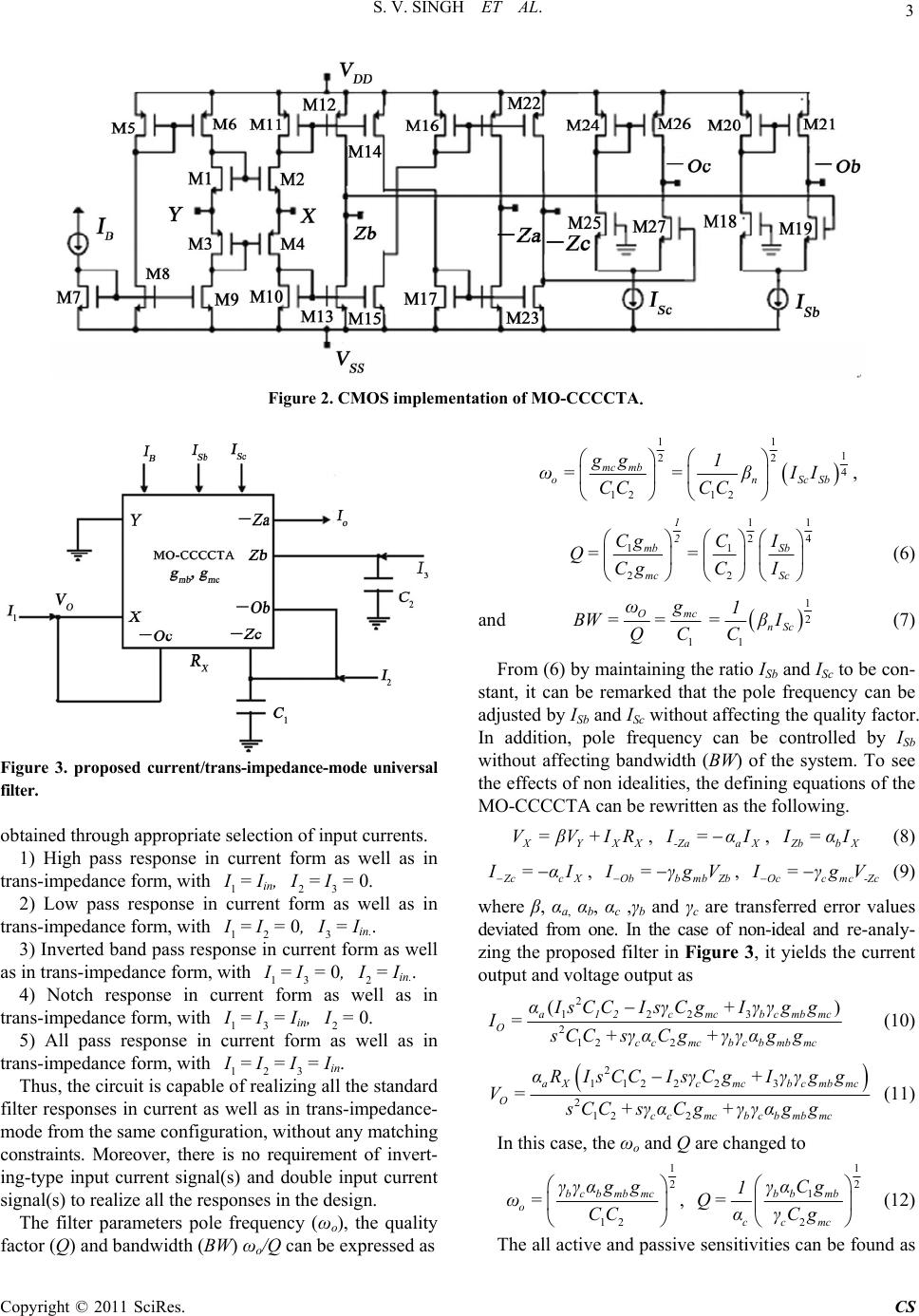 S. V. SINGH ET AL. Copyright © 2011 SciRes. CS 3 Figure 2. CMOS implementation of MO-CCCCTA. Figure 3. proposed current/trans-impedance-mode universal filter. obtained through appropriate selection of input currents. 1) High pass response in current form as well as in trans-impedance form, with 1 I = Iin, 2 I =3 I = 0. 2) Low pass response in current form as well as in trans-impedance form, with 1 I =2 I = 0, 3 I = Iin.. 3) Inverted band pass response in current form as well as in trans-impedance form, with 1 I =3 I = 0, 2 I = Iin.. 4) Notch response in current form as well as in trans-impedance form, with 1 I =3 I = Iin, 2 I = 0. 5) All pass response in current form as well as in trans-impedance form, with 1 I =2 I =3 I = Iin. Thus, the circuit is capable of realizing all the standard filter responses in current as well as in trans-impedance- mode from the same configuration, without any matching constraints. Moreover, there is no requirement of invert- ing-type input current signal(s) and double input current signal(s) to realize all the responses in the design. The filter parameters pole frequency (ωo), the quality factor (Q) and bandwidth (BW) ωo/Q can be expressed as 1 2 12 mc mb o gg ω=CC 1 1 2 4 12 nScSb 1 =βII CC , 1 2 1 2 mb mc Cg Q= Cg 1 1 4 2 1 2 Sb Sc I C =CI (6) and 1 Omc ω g BW == QC 1 2 1 nSc 1 =βI C (7) From (6) by maintaining the ratio ISb and ISc to be con- stant, it can be remarked that the pole frequency can be adjusted by ISb and ISc without affecting the quality factor. In addition, pole frequency can be controlled by ISb without affecting bandwidth (BW) of the system. To see the effects of non idealities, the defining equations of the MO-CCCCTA can be rewritten as the following. XYXX V=βV+IR , -Zaa X I=α I , Z bbX I=α I (8) Z ccX I=α I , Obbmb Zb I=γ g V , Occmc-Zc I=γ g V (9) where β, αa, αb, αc ,γb and γc are transferred error values deviated from one. In the case of non-ideal and re-analy- zing the proposed filter in Figure 3, it yields the current output and voltage output as 2 1223 2 12 2 () a12cmcb cmbmc O ccmcbcbmb mc αIsCCI sγCg +Iγγgg I= sCC +sγαCg +γγαgg (10) 2 1122 23 2 12 2 aXc mcbcmbmc O ccmcbcb mb mc αRIsCC IsγCg+Iγγgg V= sCC+sγαCg+γγαgg (11) In this case, the ωo and Q are changed to 1 2 12 bcbmbmc o γγαgg ω=CC , 1 2 1 2 bb mb ccmc γαCg 1 Q= αγCg (12) The all active and passive sensitivities can be found as  S. V. SINGH ET AL. Copyright © 2011 SciRes. CS 4 12 1 2 o ω C,C S=, 1 2 o bc bmbmc ω γ,γ,α,g ,g S=, 0 o ac X ω α,α,β,R S= (13) 2 1 2 mc c Q C,g ,γ S=, 1 1 2 bb mb Q C,α,γ,g S=, 1 c Q α S= 0 aX Q α,β,R S= (14) From the above results, it can be observed that all the active and passive sensitivities are equal or less than 1 in magnitude. 3. Simulation Results The PSPICE simulations are carried out to demonstrate the feasibility of the proposed circuit using CMOS im- plementation as shown in Figure 2. The simulations use a 0.35 µm MOSFET [30] from TSMC. The dimensions of PMOS are determined as W = 3 µm and L = 2 µm. In NMOS transistors, the dimensions are W = 3 µm and L = 4 µm. The circuit is designed for Q = 1 and fo = ωo / 2π = 1.57 MHz. The active and passive components are chosen as IB = 7.5 µA, ISb = ISc = 30.65 µA and C1 = C2 = 7.5 pF. Figure 4 Shows the simulated gain and phase responses of the HP, LP, BP, Notch and AP in the current (a) (b) (c) (d) (e) Figure 4. Current gain and Phase responses of the proposed filter (a) HP, (b) LP, (c) BP, (d) Notch and (e) AP. form, of the proposed circuit in Figure 3. The supply voltages are VDD = –VSS = 2.5 V. The simulated pole fre- quency is obtained as 1.35 MHz. It is noted that simula- tion results agree quite well with theoretical ones as ex- pected, whereas the difference between them arises from non-idealities such as non ideal gain and parasitic elements. The power dissipations of the proposed circuit for the design values is found as 0.629 mW that is a low value. Next, the frequency tuning aspect of the circuit is veri- fied for a constant Q (= 1) value for the BP response in current-mode. The bias currents ISb and ISc are varied si- multaneously, by keeping its ratio to be constant. The pole frequency variation, for Q = 1, is shown in Figure 5. The frequency is found to vary as 650 kHz, 990 kHz, 1.34 MHz and 1.8 MHz for four values of ISb = ISc = 6 µA, 15 µA, 30 µA and 60 µA, respectively. Further simula- tions are carried out to verify the total harmonic distor- tion (THD). The circuit is simulated for THD analysis at BP output in current-mode, by applying sinusoidal input current of varying amplitude and constant frequency. The THD values for the input current signal having am- plitude less than 40 µA, at frequency 1.35 MHz remain in acceptable limits i.e. 4%. The time domain response of band-pass output in current form is shown in Figure 6. It is observed that 40 µA peak to peak input current sinu- soidal signal levels are possible without significant dis- tortions. Thus both THD analysis and time domain re- sponse of BP output in current-mode confirm the prac- tical utility of the proposed circuit. 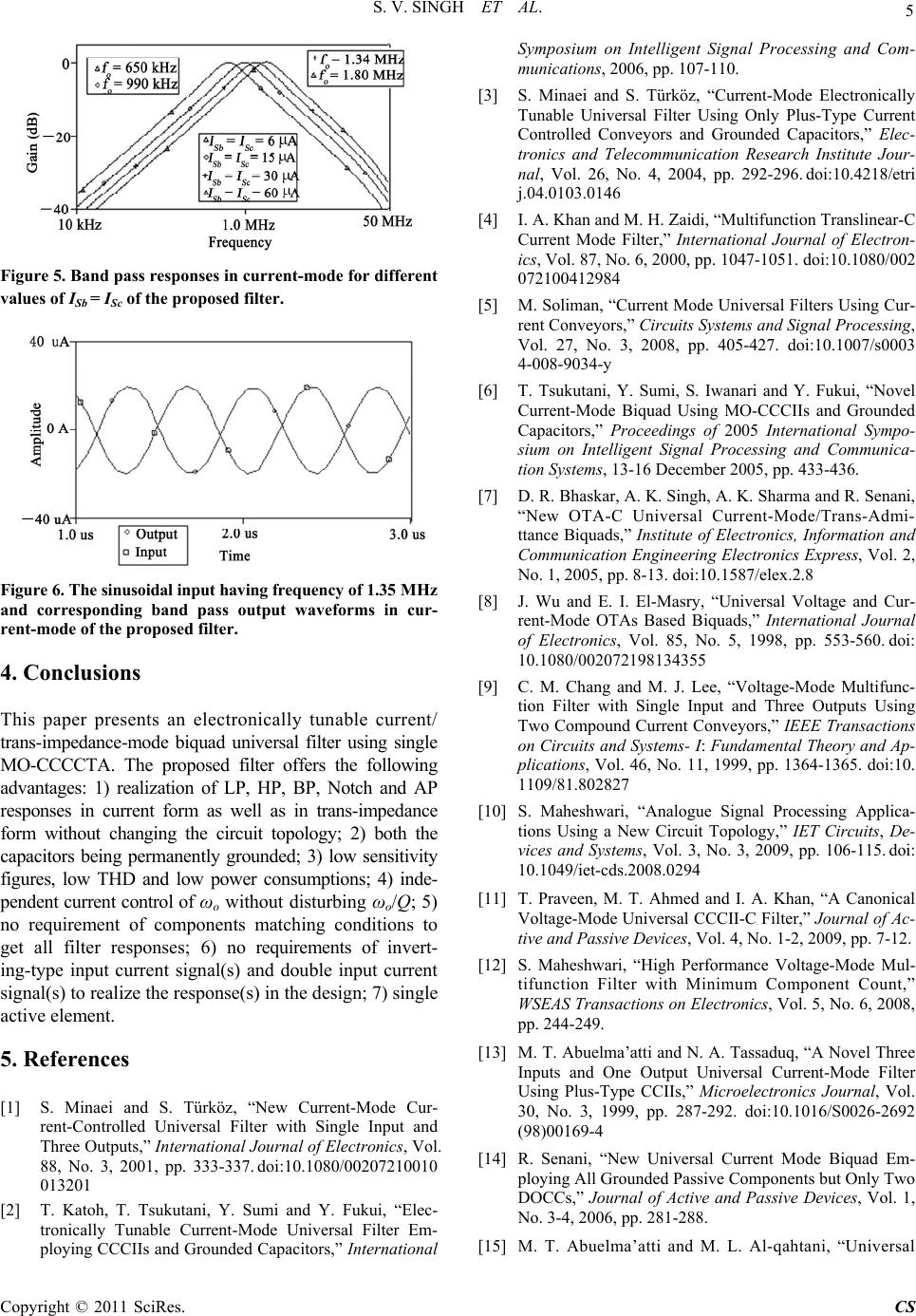 S. V. SINGH ET AL. Copyright © 2011 SciRes. CS 5 Figure 5. Band pass responses in current-mode for different values of ISb = ISc of the proposed filter. Figure 6. The sinusoidal input having frequency of 1.35 M H z and corresponding band pass output waveforms in cur- rent-mode of the proposed filter. 4. Conclusions This paper presents an electronically tunable current/ trans-impedance-mode biquad universal filter using single MO-CCCCTA. The proposed filter offers the following advantages: 1) realization of LP, HP, BP, Notch and AP responses in current form as well as in trans-impedance form without changing the circuit topology; 2) both the capacitors being permanently grounded; 3) low sensitivity figures, low THD and low power consumptions; 4) inde- pendent current control of ωo without disturbing ωo/Q; 5) no requirement of components matching conditions to get all filter responses; 6) no requirements of invert- ing-type input current signal(s) and double input current signal(s) to realize the response(s) in the design; 7) single active element. 5. References [1] S. Minaei and S. Türköz, “New Current-Mode Cur- rent-Controlled Universal Filter with Single Input and Three Outputs,” International Journal of Electronics, Vol. 88, No. 3, 2001, pp. 333-337. doi:10.1080/00207210010 013201 [2] T. Katoh, T. Tsukutani, Y. Sumi and Y. Fukui, “Elec- tronically Tunable Current-Mode Universal Filter Em- ploying CCCIIs and Grounded Capacitors,” International Symposium on Intelligent Signal Processing and Com- munications, 2006, pp. 107-110. [3] S. Minaei and S. Türköz, “Current-Mode Electronically Tunable Universal Filter Using Only Plus-Type Current Controlled Conveyors and Grounded Capacitors,” Elec- tronics and Telecommunication Research Institute Jour- nal, Vol. 26, No. 4, 2004, pp. 292-296. doi:10.4218/etri j.04.0103.0146 [4] I. A. Khan and M. H. Zaidi, “Multifunction Translinear-C Current Mode Filter,” International Journal of Electron- ics, Vol. 87, No. 6, 2000, pp. 1047-1051. doi:10.1080/002 072100412984 [5] M. Soliman, “Current Mode Universal Filters Using Cur- rent Conveyors,” Circuits Systems and Signal Processing, Vol. 27, No. 3, 2008, pp. 405-427. doi:10.1007/s0003 4-008-9034-y [6] T. Tsukutani, Y. Sumi, S. Iwanari and Y. Fukui, “Novel Current-Mode Biquad Using MO-CCCIIs and Grounded Capacitors,” Proceedings of 2005 International Sympo- sium on Intelligent Signal Processing and Communica- tion Systems, 13-16 December 2005, pp. 433-436. [7] D. R. Bhaskar, A. K. Singh, A. K. Sharma and R. Senani, “New OTA-C Universal Current-Mode/Trans-Admi- ttance Biquads,” Institute of Electronics, Information and Communication Engineering Electronics Express, Vol. 2, No. 1, 2005, pp. 8-13. doi:10.1587/elex.2.8 [8] J. Wu and E. I. El-Masry, “Universal Voltage and Cur- rent-Mode OTAs Based Biquads,” International Journal of Electronics, Vol. 85, No. 5, 1998, pp. 553-560. doi: 10.1080/002072198134355 [9] C. M. Chang and M. J. Lee, “Voltage-Mode Multifunc- tion Filter with Single Input and Three Outputs Using Two Compound Current Conveyors,” IEEE Transactions on Circuits and Systems- I: Fundamental Theory and Ap- plications, Vol. 46, No. 11, 1999, pp. 1364-1365. doi:10. 1109/81.802827 [10] S. Maheshwari, “Analogue Signal Processing Applica- tions Using a New Circuit Topology,” IET Circuits, De- vices and Systems, Vol. 3, No. 3, 2009, pp. 106-115. doi: 10.1049/iet-cds.2008.0294 [11] T. Praveen, M. T. Ahmed and I. A. Khan, “A Canonical Voltage-Mode Universal CCCII-C Filter,” Journal of Ac- tive and Passive Devices, Vol. 4, No. 1-2, 2009, pp. 7-12. [12] S. Maheshwari, “High Performance Voltage-Mode Mul- tifunction Filter with Minimum Component Count,” WSEAS Transactions on Electronics, Vol. 5, No. 6, 2008, pp. 244-249. [13] M. T. Abuelma’atti and N. A. Tassaduq, “A Novel Three Inputs and One Output Universal Current-Mode Filter Using Plus-Type CCIIs,” Microelectronics Journal, Vol. 30, No. 3, 1999, pp. 287-292. doi:10.1016/S0026-2692 (98)00169-4 [14] R. Senani, “New Universal Current Mode Biquad Em- ploying All Grounded Passive Components but Only Two DOCCs,” Journal of Active and Passive Devices, Vol. 1, No. 3-4, 2006, pp. 281-288. [15] M. T. Abuelma’atti and M. L. Al-qahtani, “Universal 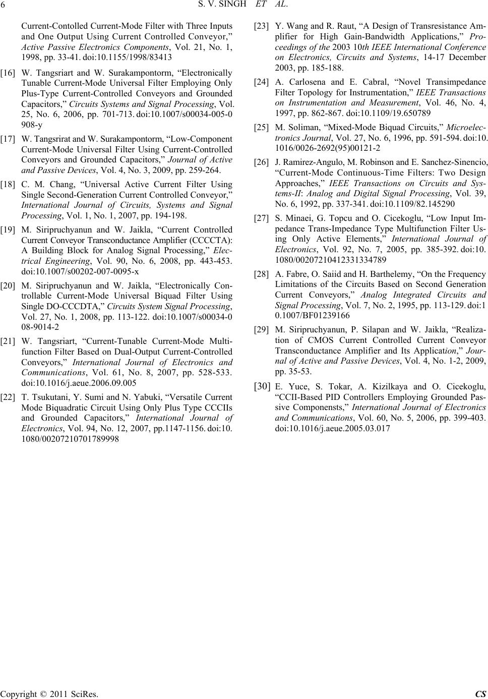 S. V. SINGH ET AL. Copyright © 2011 SciRes. CS 6 Current-Contolled Current-Mode Filter with Three Inputs and One Output Using Current Controlled Conveyor,” Active Passive Electronics Components, Vol. 21, No. 1, 1998, pp. 33-41. doi:10.1155/1998/83413 [16] W. Tangsriart and W. Surakampontorm, “Electronically Tunable Current-Mode Universal Filter Employing Only Plus-Type Current-Controlled Conveyors and Grounded Capacitors,” Circuits Systems and Signal Processing, Vol. 25, No. 6, 2006, pp. 701-713. doi:10.1007/s00034-005-0 908-y [17] W. Tangsrirat and W. Surakampontorm, “Low-Component Current-Mode Universal Filter Using Current-Controlled Conveyors and Grounded Capacitors,” Journal of Active and Passive Devices, Vol. 4, No. 3, 2009, pp. 259-264. [18] C. M. Chang, “Universal Active Current Filter Using Single Second-Generation Current Controlled Conveyor,” International Journal of Circuits, Systems and Signal Processing, Vol. 1, No. 1, 2007, pp. 194-198. [19] M. Siripruchyanun and W. Jaikla, “Current Controlled Current Conveyor Transconductance Amplifier (CCCCTA): A Building Block for Analog Signal Processing,” Elec- trical Engineering, Vol. 90, No. 6, 2008, pp. 443-453. doi:10.1007/s00202-007-0095-x [20] M. Siripruchyanun and W. Jaikla, “Electronically Con- trollable Current-Mode Universal Biquad Filter Using Single DO-CCCDTA,” Circuits System Signal Processing, Vol. 27, No. 1, 2008, pp. 113-122. doi:10.1007/s00034-0 08-9014-2 [21] W. Tangsriart, “Current-Tunable Current-Mode Multi- function Filter Based on Dual-Output Current-Controlled Conveyors,” International Journal of Electronics and Communications, Vol. 61, No. 8, 2007, pp. 528-533. doi:10.1016/j.aeue.2006.09.005 [22] T. Tsukutani, Y. Sumi and N. Yabuki, “Versatile Current Mode Biquadratic Circuit Using Only Plus Type CCCIIs and Grounded Capacitors,” International Journal of Electronics, Vol. 94, No. 12, 2007, pp.1147-1156. doi:10. 1080/00207210701789998 [23] Y. Wang and R. Raut, “A Design of Transresistance Am- plifier for High Gain-Bandwidth Applications,” Pro- ceedings of the 2003 10th IEEE International Conference on Electronics, Circuits and Systems, 14-17 December 2003, pp. 185-188. [24] A. Carlosena and E. Cabral, “Novel Transimpedance Filter Topology for Instrumentation,” IEEE Transactions on Instrumentation and Measurement, Vol. 46, No. 4, 1997, pp. 862-867. doi:10.1109/19.650789 [25] M. Soliman, “Mixed-Mode Biquad Circuits,” Microelec- tronics Journal, Vol. 27, No. 6, 1996, pp. 591-594. doi:10. 1016/0026-2692(95)00121-2 [26] J. Ramirez-Angulo, M. Robinson and E. Sanchez-Sinencio, “Current-Mode Continuous-Time Filters: Two Design Approaches,” IEEE Transactions on Circuits and Sys- tems-II: Analog and Digital Signal Processing, Vol. 39, No. 6, 1992, pp. 337-341. doi:10.1109/82.145290 [27] S. Minaei, G. Topcu and O. Cicekoglu, “Low Input Im- pedance Trans-Impedance Type Multifunction Filter Us- ing Only Active Elements,” International Journal of Electronics, Vol. 92, No. 7, 2005, pp. 385-392. doi:10. 1080/00207210412331334789 [28] A. Fabre, O. Saiid and H. Barthelemy, “On the Frequency Limitations of the Circuits Based on Second Generation Current Conveyors,” Analog Integrated Circuits and Signal Processing, Vol. 7, No. 2, 1995, pp. 113-129. doi:1 0.1007/BF01239166 [29] M. Siripruchyanun, P. Silapan and W. Jaikla, “Realiza- tion of CMOS Current Controlled Current Conveyor Transconductance Amplifier and Its Application,” Jour- nal of Active and Passive Devices, Vol. 4, No. 1-2, 2009, pp. 35-53. [30] E. Yuce, S. Tokar, A. Kizilkaya and O. Cicekoglu, “CCII-Based PID Controllers Employing Grounded Pas- sive Componensts,” International Journal of Electronics and Communications, Vol. 60, No. 5, 2006, pp. 399-403. doi:10.1016/j.aeue.2005.03.017 |